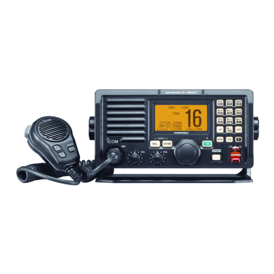
Icom IC-M604 Service Manual
Vhf marine transcever
Hide thumbs
Also See for IC-M604:
- Instruction manual (65 pages) ,
- Service manual (8 pages) ,
- Instruction manual (64 pages)
Table of Contents
Advertisement
Advertisement
Table of Contents

Related Manuals for Icom IC-M604


Summary of Contents for Icom IC-M604
- Page 1 SERVICE MANUAL VHF MARINE TRANSCEVER iC-m604 S-14306MZ-C1 Aug. 2006...
- Page 2 8. READ the instructions of test equipment thoroughly before connecting equipment to the transceiver. Icom, Icom Inc. and logo are registered trademarks of Icom Incorporated (Japan) in the United States, the United Kingdom, Germany, France, Spain, Russia and/or other countries.
-
Page 3: Table Of Contents
IC-M604 ........ -
Page 4: Specifications
SECTION 1 SPECIFICATIONS ¤ GENERAL • Frequency coverage : 156.025–157.425 MHz (TX) 156.050–163.275 MHz (RX) • Mode : 16K0G3E (FM) / 16K0G2B (DSC) • Power supply voltage : 13.8 V DC ±15 % (negative ground) • Operating temperature range : –20˚C to +60˚C; –4˚F to +140˚F •... -
Page 5: Vhf Marine Channel List
¤ VHF MARINE CHANNEL LIST . y l . y l , s l y l l c i l 1 - 2... -
Page 6: Inside Views
SECTION 2 INSIDE VIEWS 2-1 IC-M604 • MAIN UNIT RF amplifier (Q1: 3SK294) RF amplifier (for CH70) (Q7: 3SK294) Antenna switch circuit 1st mixer circuit 1st mixer circuit (for CH70) D11: HSB88WS D21: HSB88WS L18: 617DB-1919=P3 L48, L49: 617DB-1327=P3 L19: 617DB-1327=P3... -
Page 7: Hm-157 (Optional Product)
2-2 HM-157 (Optional product) • TOP VIEW (DS1: A0119) • BOTTOM VIEW System clock (X1: CSTCC4.91MG) (IC1: PD789405AGK-A30-9EU) Dimmer circuit Data buffer circuit Reset IC 8V regulator (IC7: S-80928CNMC) (IC6: TA7808F) 5V regulator Volume IC (IC5: TA78L05F) (IC3: M62429FP) AF/MIC switch (IC9: TC4W53FU) AF amplifier MIC amplifier... - Page 8 SECTION 3 DISASSEMBLY AND OPTIONS INSTRUCTIONS 1. Opening the transceiver case 3. Removing the MAIN UNIT 1 Unscrew 6 screws A, and remove the front unit. 1 Remove the shield cover E. 2 Unscrew 6 screws B, and remove the rear panel. REAR panel FRONT UNIT 2 Disconnect flat cables from J1 and J2.
-
Page 9: Circuit Description
SECTION 4 CIRCUIT DESCRIPTION 4-1 RECEIVER CIRCUITS 4-1-3 1ST MIXER AND 1ST IF CIRCUITS 4-1-1 ANTENNA SWITCHING CIRCUIT (MAIN UNIT) (MAIN UNIT) The antenna switching circuit functions as a low-pass filter The 1st mixer circuit converts the received signal into a while receiving and as resonator circuit while transmitting. - Page 10 4-1-4 2ND IF AND DEMODULATOR CIRCUITS The FM detector circuit employs a quadrature detection method (linear phase detection), which uses a ceramic dis- (MAIN UNIT) criminator (X2) for phase delay to obtain a non-adjusting The 2nd mixer circuit converts the 1st IF signal into a 2nd IF circuit.
-
Page 11: Transmitter Circuits
4-1-5 AF AMPLIFIER CIRCUIT (AF UNIT) The amplified signals are applied to the IDC amplifier (IC8a, pin 2) via the analog switch (IC7, pins 2, 3, 9), and are then The AF amplifier circuit amplifies the demodulated signals passed through the splatter filter (IC8b) to suppress unwant- to drive a speaker. -
Page 12: Pll Circuits
4-2-5 APC CIRCUIT (MAIN UNIT) 4-3-2 TX AND CHANNEL 70 (RX) LOOPS The APC (Automatic Power Controller) circuit stabilizes the The generated signal at the TX-VCO/CHANNEL 70-VCO TX output power. (Q18, D37, D39, D40) enters the PLL IC (IC12, pin 2) and is divided at the programmable divider section and is then The RF output signal from the power amplifier (IC13) is applied to the phase detector section. -
Page 13: Dsc Circuits
4-3-4 VCO CIRCUIT (MAIN UNIT) The signalis passed through the splatter filter (AF unit; IC8b) to suppress unwanted 3 kHz or higher signals. The filtered • TX-VCO/CHANNEL 70-VCO (RX) CIRCUITS signals are then applied to the TX modulation circuit via the The VCO outputs from TX-VCO/CHANNEL 70-VCO (Q18) D/A converter IC (MAIN unit;... -
Page 14: Power Supply Circuits
4-6 POWER SUPPLY CIRCUITS 4-7 PORT ALLOCATIONS 4-6-1 VOLTAGE LINE (MAIN UNIT) 4-7-1 EXPANDER IC (AF unit; IC18) Port DESCRIPTION LINE Description number name The 13.8 V from the connected DC power sup- Outputs HM-162/2 control signal. ply. MICS2 High : While transmitting via the Same voltage as the 13.8 V line, and is applied HM-162/2. - Page 15 4-7-3 CPU (LOGIC BOARD; IC1) Port Port Description Description number name number name Input port for PLL unlock signal from Input port for the low-battery detecting UNLK the PLL IC (MAIN unit; IC12, pin 7). signal. Low battery indicator appears LBAT High : While PLL is unlocked.
-
Page 16: Adjustment Procedures
SECTION 5 ADJUSTMENT PROCEDURES 5-1 PREPARATION ¤ REQUIRED TEST EQUIPMENT EQUIPMENT GRADE AND RANGE EQUIPMENT GRADE AND RANGE Output voltage : 13.8 V DC Frequency range : 0.1–300 MHz DC power supply Standard signal Current capacity : 10 A or more Output level : 0.1 µV to 32 mV generator (SSG) -
Page 17: Pll Adjustments
5-2 PLL ADJUSTMENTS ADJUSTMENT MEASUREMENT POINT ADJUSTMENT ADJUSTMENT CONDITION VALUE UNIT LOCATION UNIT ADJUST LOCK • Operating channel : ch P2 MAIN Connect a digital 3.8 V – 4.0 V MAIN VOLTAGE • Receiving multi-meter or oscil- loscope to check point CP1. -
Page 18: Receiver Adjustments
5-3 RECEIVER ADJUSTMENTS ADJUSTMENT MEASUREMENT POINT ADJUSTMENT ADJUSTMENT CONDITION VALUE UNIT LOCATION UNIT ADJUST SENSITIVITY • Operating channel : ch 16 MAIN Connect a tracking Set the flat wave form MAIN (Except chan- • Connect a tracking generator’s generator’s input to as shown below. - Page 19 • MAIN UNIT TOP VIEW • MAIN UNIT TOP VIEW RX sensitivity adjustment for channel 70 RX sensitivity adjustment for other channels RX sensitivity check point 5 - 4...
-
Page 20: Parts List
SECTION 6 PARTS LIST [LOGIC UNIT] • IC-M604 [REPLACEMENT UNITS] ORDER DESCRIPTION LOCATION ORDER NO. UNIT NAME COLOR 7030003360 S.RES ERJ3GEYJ 221 V (220) 103.8/13 7030003360 S.RES ERJ3GEYJ 221 V (220) 107.1/49.6 0325770121 U M604 #21 FRONT (including LOGIC UNIT) BLACK 7030003360 S.RES ERJ3GEYJ 221 V (220) -
Page 21: Af Unit
[LOGIC UNIT] [AF UNIT] ORDER ORDER DESCRIPTION DESCRIPTION LOCATION LOCATION C110 4030007090 S.CER C1608 CH 1H 470J-T 86.6/84.3 1110002031 IC TA7808S (Q) C111 4030007090 S.CER C1608 CH 1H 470J-T 87.5/73.6 1180000421 S.IC TA78L05F (TE12) 37.2/31.5 C112 4030007090 S.CER C1608 CH 1H 470J-T 87.9/84.3 1110003091 IC LA4425A-E... - Page 22 [AF UNIT] [AF UNIT] ORDER ORDER DESCRIPTION DESCRIPTION LOCATION LOCATION 7030003800 S.RES ERJ3GEYJ 105 V (1 M) 91.3/2.8 R302 7030003460 S.RES ERJ3GEYJ 152 V (1.5 k) 7.2/30.5 7030003800 S.RES ERJ3GEYJ 105 V (1 M) 113.4/10.5 R303 7030009591 S.RES ERA3YED 472V (4.7 k) 7.2/27.5 7030003800 S.RES ERJ3GEYJ 105 V (1 M) 102/3.5...
- Page 23 [AF UNIT] [MAIN UNIT] ORDER ORDER DESCRIPTION DESCRIPTION LOCATION LOCATION 4030008900 S.CER C1608 JB 1H 333K-T 61.4/6.2 1110003491 S.IC TA31136FNG (D EL) 113.7/6.5 4030006900 S.CER C1608 JB 1H 103K-T 68.1/6.2 1120002830 S.IC NJM2125F-TE1 147.9/9.3 4030011600 S.CER C1608 JB 1E 104K-T 66.8/6.2 1110003780 S.IC NJM2902V-TE1...
- Page 24 [MAIN UNIT] [MAIN UNIT] ORDER ORDER DESCRIPTION DESCRIPTION LOCATION LOCATION 6190001591 COL #E526HNA-100312 7030003560 S.RES ERJ3GEYJ 103 V (10 k) 148.1/32.7 6140002551 S.COL #617DB-1919=P3 53.2/6.2 7030003560 S.RES ERJ3GEYJ 103 V (10 k) 150.5/31 6130002961 S.COL #617DB-1327=P3 64.8/6.2 7030003560 S.RES ERJ3GEYJ 103 V (10 k) 157/33.6 6200001831 S.COL NLV32T-100J 75.9/8...
- Page 25 [MAIN UNIT] [MAIN UNIT] ORDER ORDER DESCRIPTION DESCRIPTION LOCATION LOCATION R257 7030003440 S.RES ERJ3GEYJ 102 V (1 k) 69.4/33.9 4030011600 S.CER C1608 JB 1E 104K-T 14.3/21.3 R258 7030003270 S.RES ERJ3GEYJ 390 V (39) 81.2/44.8 4030009920 S.CER C1608 CH 1H 050B-T 8/15.6 R259 7030003480 S.RES ERJ3GEYJ 222 V (2.2 k)
- Page 26 [MAIN UNIT] [MAIN UNIT] ORDER ORDER DESCRIPTION DESCRIPTION LOCATION LOCATION C187 4030011600 S.CER C1608 JB 1E 104K-T 146/42.6 C319 4030006860 S.CER C1608 JB 1H 102K-T 73.3/35.8 C190 4030011600 S.CER C1608 JB 1E 104K-T 146/47.6 C320 4030006860 S.CER C1608 JB 1H 102K-T 74.9/33 C191 4030008850 S.CER C1608 JB 1H 123K-T...
- Page 27 [MAIN UNIT] [SQL UNIT] ORDER ORDER DESCRIPTION DESCRIPTION LOCATION LOCATION 7210002360 VAR TP96N97-15F-10KB-1301 6510007020 CNR TMP-J01X-V6 M.=Mounted side (T: Mounted on the Top side, B: Mounted on the Bottom side) S.=Surface mount 7030010840 S.JMP MJP-0.2-T 72.7/50.9 7030010860 JMP MJP-0.6 6910013370 S.BEA BLM18BB221SN1D 71.2/21 6910002161 CAS...
- Page 28 [MAIN UNIT] • HM-126RB/RG ORDER [REPLACEMENT UNITS] DESCRIPTION LOCATION ORDER NO. UNIT NAME COLOR 7030003280 S.RES ERJ3GEYJ 470 V (47) 31.6/40.3 7030003580 S.RES ERJ3GEYJ 153 V (15 k) 29.8/8.2 Optional product HM-126RB [USA] BLACK 7030003560 S.RES ERJ3GEYJ 103 V (10 k) 29/10.1 Optional product HM-126RG...
-
Page 29: Front Unit
SECTION 7 MECHANICAL PARTS IC-M604 [FRONT UNIT] [CHASSIS PARTS] REF. NO. ORDER NO. DESCRIPTION QTY. REF. NO. ORDER NO. DESCRIPTION QTY. 2510001210 SPEAKER 066P0804 6510004880 Antenna connector MR-DSE-01 8900015550 Cable OPC-1658 8900015950 Cable OPC-1175A 8900011460 Cable OPC-1176 8210023090 2577 front panel (C) assembly... - Page 30 MP13 (C) MP14 (C) MP19 (C) Unit abbreviations (C): CHASSIS PARTS MP8 (C) (M): MAIN UNIT MP2 (C) MP7 (C) (F): FRONT UNIT (L): LOGIC BOARD IC13 (M) (A): AF UNIT (CO): CONNECT UNIT (D): DIAL BOARD (S): SQL BOARD MP4 (M) MP11 (C) MP5 (M)
-
Page 31: Hm-126Rb/Rg
2352 mic plate MP12 8930053750 2417 plate MP1 (C) MP12 8820001150 2352 screw MP13 8210017250 2417 rear panel-1 MP13 8850001850 ICOM washer (Y) 8210022021 2417 rear panel (C)-1 [SW] MP7 (C) MP14 8930052340 O-ring (AE) MP14 8310049970 2417 R-plate MP15 8930052350... - Page 32 SECTION 8 SEMI-CONDUCTOR INFORMATION • TRANSSISTORS AND FET’S • DIODES 2SA1576A T106 R 2SA1577 T106 Q 2SB1132 T100 R 2SB1143 S 1SS355 1SS372 1SV214 1SV288 1SV307 2SC3326 B (Symbol: FR) (Symbol: HQ) (Symbol: BAR) (Symbol: B1143) (Symbol: A) (Symbol: N9) (Symbol: T1) (Symbol: TJ) (Symbol: TX)
- Page 33 SECTION 9 BOARD LAYOUTS to AF unit J4 to LOGIC unit J6 9-1 VR UNIT (TOP VIEW) 9-4 CONNECT UNIT (TOP VIEW) VOL2 VOL1 to AF unit J6 to AF unit W6 9-2 SQL UNIT (TOP VIEW) SQL5V SQLV SQLG to LOGIC unit J7 •...
- Page 34 The combination of this page and the next page shows the unit layout in the same configuration as the actual P.C. Board. 9-5 LOGIC UNIT (TOP VIEW) MENU CH/WX DISTRESS POWER H100 H105 H110 H115 H120 H125 H130 H135 H140 H145 H150 9 - 2...
- Page 35 to MAIN unit J1 The combination of this page and the previous page shows the unit layout in the same configuration as the actual P.C. Board. to LCD 9-5 LOGIC UNIT (BOTTOM VIEW) to CONNECT unit J6 Internal speaker (CHASSIS: SP1) to DIAL/SQL unit W1 to FRONT unit W1 to FRONT unit W7...
- Page 36 The combination of this page and the next page shows the unit layout in the same configuration as the actual P.C. Board. to LOGIC unit J1 TXDET SEND DADATA TMUTE 9-6 MAIN UNIT (TOP VIEW) ATT2 ATT1 UNLK PSTB PDATA CHASSIS DEC2 RXDDJ...
- Page 37 The combination of this page and the previous page shows the unit layout in the same configuration as the actual P.C. Board. • MAIN UNIT (BOTTOM VIEW) H160 H155 H150 H145 H140 H135 H130 H125 H120 H115 H110 H105 H100 9 - 5...
- Page 38 The combination of this page and the next page shows the unit layout in the same configuration as the actual P.C. Board. 9-7 AF UNIT (TOP VIEW) to CHASSIS W1 to Optional (OPC-1175) to CONNECT unit J4 unit UT-112 to CHASSIS W2 HALL+ (OPC-1176) HALL-...
- Page 39 The combination of this page and the previous page shows the unit layout in the same configuration as the actual P.C. Board. to MAIN unit • AF UNIT (BOTTOM VIEW) H160 H155 H150 H145 H140 H135 H130 H125 H120 H115 H110 H105 H100...
- Page 40 The combination of this page and the next page 9-8 HM-126RB/RG (TOP VIEW) shows the unit layout in the same configuration as the actual P.C. Board. to Speaker 9-9 HM-157 (Optional product) (TOP VIEW) MICE to FRONT unit W1 to Microphone 9 - 8...
- Page 41 The combination of this page and the previous page shows the unit layout in the same configuration as the actual P.C. Board. • HM-126RB-RG (BOTTOM VIEW) • HM-157 (Optional product) (BOTTOM VIEW) SCAN PWRC RRXDA RTXDA PTTC MICG AF/MIC 16/9 to CONNECT unit J1 to Speaker...
-
Page 42: Block Diagram
SECTION 10 BLOCK DIAGRAM FI3 CFWM450E CHASSIS UNIT MAIN UNIT Q2 2SC4215 Q3,4 HM-126R CERAMIC D15 MA742 FL-404 PMBFJ310x2 3SK294 HSB88WS IC1 TA31136FNG XTAL D12 MA8036 X1 CDBKB450KCAY24 IC3a 30.15MHz NJM2902V 2SC4116 2SC5110 WXDEC 2ND IF RIPPLE BUFF Q16 2SC4116 2SC4215 IC4 NJM2211M IC3b NJM2902V... -
Page 43: Wiring Diagram
SECTION 11 WIRING DIAGRAM HANG OPC-1212 MICG FRONT UNIT OPC-1658 W1 OPC-1175 MICG VR UNIT OPC-1176 VOL1 VOL2 HAIL+ HAIL+ HAIL- HAIL- VOL1 OPC-1186 CHASSIS VOL2 KPWRH2 KPWRH2 CMDPWR2 CMDPWR2 OPC-1659 ICF3 ICF3 CMDPWR1 CMDPWR1 NMEAOUT+ CVCC CVCC CVCC CVCC SCOUT SCOUT CVCC... -
Page 44: Voltage Diagram
SECTION 12 VOLTAGE DIAGRAMS 12-1 LOGIC UNIT 3.3V TC74LCXR164245 CP06VR 1DIR LDB7 LDB6 LDB5 LDB4 RXADJ VCCB VCCA WXDEC LDB3 LDB2 KTC2875 LDB1 DATAMC 27FLZ-SM2-TB LDB0 CS1B 1SS372 RESETB RW_WR 26FLT-SM2-TB E_RD TEMP TEMP VCCB VCCA WXDEC LRESETB DATACM RXADJ DEC1 DEC1 LCS1B... -
Page 45: Main Unit
12-2 MAIN UNIT 1.25V at –8dB NJM2125F R313 CP12 CP10S CP10S CP10S RSSI 4.7H R309 WXDEC NJM2902V 0.01 #E526HNA C109 C108 C107 C102 NJM2902V 0.01 0.01 0.01 0.001 2SC4215 PMBFJ310 R306 HSB88WS #617DB #617DB 3.74V NJM2902V CDBC450CX24 1.5P 2.5P IC4 NJM2211M C111 C118 FI1B... -
Page 46: Af Unit
12-3 AF UNIT 13.70V OP-10 PWRON PWRON PWRON OPC-1175 CHASSIS 2SA1577 UNIT OP-10 FTR-P3CP012W1 4.97V 8.02V 2SB1132 TA78L05F TA7808S DTC144EU TX: 0V RX: 4.93V DTC144EU 2.2K SB4P-HVQ-A 13.68V C270 2P-SZN OPTION SP– TO MAIN CONNECT UNIT UNIT J5 OPC-1203 R202 C208 INTERNAL SP-ON: 4.87V 1SS355... -
Page 47: Hm-126Rb/Rg
12-4 HM-126RB/RG UP KEY : 2.0V DOWN KEY : 3.0V 16/9 KEY : 3.8V 6.8k W1 (CHASSIS) DOWN 16/9 HANGER 470p 470p 12 - 4... -
Page 48: Hm-157 (Optional Product)
DIM2 CP11 P44/KR4 SEG15 DIM3 P45/KR5 SEG16 AF/MIC P93/S16 SEG17 MICG P92/S17 NTCG16 SEG18 P91/S18 0.01 0.001 CP14 to IC-M604 TA78L05F SEG19 PTTC P90/S19 PD789405AGK-A30-9EU VDD0 CP15 CONNECT unit J1 SEG20 RTXDA P87/S20 VSS0 SEG21 RRXDA P86/S21 CP18 SEG22 PWRC... - Page 49 Phone : +34 (93) 590 26 70 Fax : +34 (93) 589 04 46 Glenwood Centre #150-6165 : http://www.icomspain.com Highway 17 Delta, B.C., V4K 5B8, Canada E-mail : icom@icomspain.com Phone : +1 (604) 952-4266 Fax : +1 (604) 952-0090 : http://www.icomcanada.com E-mail : info@icomcanada.com Unit 9, Sea St., Herne Bay, Kent, CT6 8LD, U.K.
- Page 50 S-14306MZ-C1 1-1-32, Kamiminami, Hirano-ku, Osaka 547-0003, Japan © 2006 Icom Inc.