Table of Contents
Advertisement
Quick Links
Advertisement
Table of Contents

Related Manuals for SOYO 82430 VX PCI


Summary of Contents for SOYO 82430 VX PCI
- Page 1 Pentium 82430 VX/P54C PCI Mainboard User’s Guide & Technical Reference 5VX0/X2/X5...
-
Page 2: About This Guide
It is the policy of Soyo Computer Inc. to respect the valid patent rights of third parties and not to infringe upon or assist others to infringe upon such rights. -
Page 3: Table Of Contents
Table of Contents Chapter 1: Introduction ............1 Key Features ..................1 Unpacking the Mainboard ..............2 Electrostatic Discharge Precautions............. 2 Mainboard Layout w/ Default Settings ..........3 Chapter 2: Hardware Setup ............ 5 Jumpers ....................5 JP3: Display Type ................5 JP5: CMOS Clear Jumper .............. - Page 4 IDE1/IDE2 Ð On-board Primary/Secondary IDE HDD Connectors ..................15 JP15 Ð IR Connector ..............16 J17 Ð Keylock & Power LED Connector ........16 J26, J27 Ð PS/2 Mouse, PS/2 Keyboard Connector...... 16 PRT Ð Parallel Port Connector ............. 16 J23: Sleep Switch Connector Enable/Disable ......
-
Page 5: Chapter 1: Introduction
1 Introduction The 82430 VX PCI mainboard is a high-performance multimedia and ATX form-factor system board that supports P54CX/P55CX family CPUs. You can order 256K or 512K of external cache memory on the mainboard. The mainboard is fully compatible with industry standards, and adds many technical enhancements. -
Page 6: Unpacking The Mainboard
Introduction Unpacking the Mainboard The mainboard package contains: ¥ The 82430VX / P54C Mainboard ¥ This User's Guide ¥ One IDE Bus Master driver and three audio drivers diskettes Note: Do not unpack the mainboard until you are ready to install it. Follow the precautions below while unpacking the mainboard. -
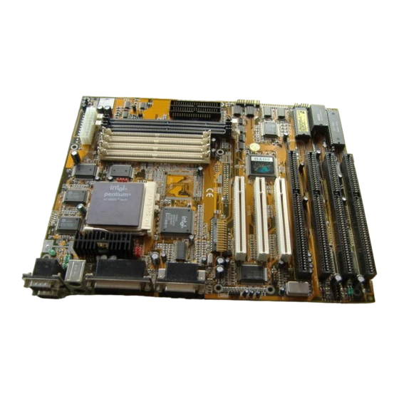
Page 7: Mainboard Layout W/ Default Settings
Introduction Mainboard Layout w/ Default Settings Figure 1Ð1. Mainboard Layout 1. P54C in ZIF socket 7 13. IDE1/IDE2 Connector 2. 82430 VX Chipset 14. Wave Table Connector 3. Pipelined Burst SRAM 15. AT Power Connector (Reserved) 4. Creative CT2505 chip 16. - Page 8 Introduction Default settings are as follows: Pentium 100MHz CPU, 256K Pipelined Burst cache, On-board PCI E-IDE Enabled, 2 high speed UARTS Enabled (w/ 16550 FIFO), 1 EPP/ECP port (ECP + EPP mode), and 5V DRAM/3.3V DIMM. LINE PS/2 KB COM1 Conn.
-
Page 9: Chapter 2: Hardware Setup
2 Hardware Setup This chapter explains how to configure the mainboardÕs hardware. After you install the mainboard, you can set jumpers, install memory on the mainboard, and make case connections. Refer to this chapter whenever you upgrade or reconfigure your system. CAUTION: Turn off power to the mainboard, system chassis, and peripheral devices before performing any work on the... -
Page 10: Jps2: Ps/2 Mouse Function Jumper
Hardware Setup JPS2: PS/2 Mouse Function Jumper Set PS/2 mouse function enabled or disabled. PS/2 Mouse Function JPS2 Disabled (default) Enabled Note: The IRQ12 is dedicated to the PS/2 mouse when choosing enabled of PS/2 Mouse Function. -
Page 11: Cpu Type Configuration
Hardware Setup CPU Type Configuration This section shows you how to configure your CPU step by step. Note that you need to check the CPU voltage before installation. Step 1: Frequency Setting Pentium – 75/90/100 CPU Settings (1.5 x clock) AMD K5 –... -
Page 12: Pentium Ð 100/120/133 Cpu Settings (2.0 X Clock)
Hardware Setup Pentium – 100/120/133 CPU Settings (2.0 x clock) Cyrix 6x86/6x86L – P120 + /P133 +/ P150 + /P166 + CPU Settings (2.0 x clock) Pentium – 100/50 MHz Cyrix 6x86/6x86L – P120 + /50 MHz JP12 JP11 JP10 Cyrix 6x86/6x86L –... -
Page 13: Pentium/Amd Ð 150/166 Cpu Settings (2.5 X Clock)
Hardware Setup Pentium/AMD – 150/166 CPU Settings (2.5 x clock) Pentium – 150/60 MHz AMD K5 – PR150 JP12 JP11 JP10 JP12 JP11 P.B. SRAM 32k x 32 JP10 Family P.B. SRAM 32k x 32 Pentium – 166/66 MHz AMD K5 – PR166 JP13 JP14 JP12... -
Page 14: Step 2: Cpu Single/Dual Voltage Setting
Hardware Setup Step 2: CPU Single/Dual Voltage Setting Single Voltage CPU Setting Signal voltage CPUs use the same voltage for VIO and VCore and has been used traditionally. The CPUs which fall into this category are Intel P54CX, AMD-K5-PRxxxBx, AMD-K5-PRxxxCx, AMD-K5-PRxxxFx, and Cyrix 6x86. -
Page 15: Dual Voltage Cpu Setting
Hardware Setup Dual Voltage CPU Setting Dual voltage CPUs are designed to use different voltage for VIO and VCore and they include Intel P55CX, AMD-K5-PRxxxHx, AMD-K5- PRxxxJx, AMD-K5-PRxxxKx, AMD K6, Cyrix 6x86L, and Cyrix M2. Refer to the following figures to set these CPUsÕ voltage: 2.5V CPU JP47 JP46... -
Page 16: Memory Configuration
Hardware Setup Memory Configuration The mainboard supports two banks of 72-pin SIMM, EDO DRAM, and two strips of 3.3V/5V Unbuffered DIMM. The mainboard requires SIMM of at least 70ns access time. The mainboard supports from 4 to 128 Mbytes with no other restrictions on memory configurations. -
Page 17: Cache Configuration
Hardware Setup Cache Configuration The mainboard has a write-back caching scheme. You can order 256KB or 512KB Level 2 Pipelined Burst cache onboard to improve the system performance. Cache Size and RAM Locations Cacheable Cache Size Cache RAM TAG RAM Range 256KB 32K x32, 2 pcs... -
Page 18: Connectors
Hardware Setup Connectors Attach the mainboard to case devices, or an external battery, via connectors on the mainboard. Refer to Figure 1-1 for connector locations and connector pin positions. ATX PW — ATX Power Supply Connectors The motherboard provides an ATX power supply connector. It is a twenty-pin male header connector. -
Page 19: J7 Ð Cd In Connector
Hardware Setup J7 – CD In Connector Connect a 4-pin audio cable, which is provided by the CD-ROM manufacture, from the Audio-out port of the CD-ROM drive to this connector, and also for transferring the audio signal from the CD-ROM to the speakers system, connect speakers system audio-in cable to speaker out jack of this mainboard. -
Page 20: Jp15 Ð Ir Connector
Hardware Setup JP15 – IR Connector Attach a 4-pin infrared device cable to this connector for enabling the infrared transfer function. This mainboard meets the specification of ASKIAR and HPSIR. J17 – Keylock & Power LED Connector J17 is a connector for a lock that may be installed on the system case for enabling or disabling the keyboard. -
Page 21: J2, J3 Ð Universal Serial Bus Connector (Optional)
Hardware Setup J2, J3 – Universal Serial bus Connector (Optional) Attach USB cable to these connectors for external USB device. JP52 – Wave Table Connector Attach Wave Table card or Wave Table daughter board to this connector. -
Page 22: Chapter 3: Bios Setup
3 BIOS Setup The mainboardÕs BIOS setup program is the ROM PCI/ISA BIOS from Award Software Inc. Enter the Award BIOS programÕs Main Menu as follows: 1. Turn on or reboot the system. After a series of diagnostic checks, you are asked to press DEL to enter Setup. -
Page 23: Standard Cmos Setup
BIOS Setup Standard CMOS Setup Run the Standard CMOS Setup as follows. 1. Choose ÒSTANDARD CMOS SETUPÓ from the Main Menu. A screen appears. ROM PCI/ISA BIOS STANDARD CMOS SETUP AWARD SOFTWARE, INC. Date (mm:dd:yy) : Fri, Feb 1 1995 Time (hh:mm:ss) : 7 : 30 : 33 HARD DISKS... -
Page 24: Bios Features Setup
BIOS Setup BIOS Features Setup Run the BIOS Features Setup as follows. 1. Choose ÒBIOS FEATURES SETUPÓ from the Main Menu and a screen with a list of items appears. (The screen below shows the BIOS default settings.) ROM PCI/ISA BIOS BIOS FEATURES SETUP AWARD SOFTWARE, INC. - Page 25 BIOS Setup Boot Sequence The default setting attempts to first boot from drive A:, drive C, or CD-ROM. You can reverse this sequence with ÒC: A:Ó, but then drive A: cannot boot directly. (It depends on the specifications of CD- ROM or CD-ROM drivers to boot from CD-ROM.) Swap Floppy Enabled changes the sequence of the A: and B:...
- Page 26 BIOS Setup OS Select for OS2: Choosing this when you are using OS/2 DRAM >64MB operation system. Non-OS/2: Choosing this when you are using no- OS/2 operation system. Video or BIOS shadow copies BIOS code from slower ROM Adapter BIOS to faster RAM.
-
Page 27: Chipset Features Setup
BIOS Setup Chipset Features Setup The Chipset Features Setup option changes the values of the chipset registers. These registers control system options in the computer. Note: Change these settings only if you are familiar with the Chipset. Run the Chipset Features Setup as follows. 1. - Page 28 BIOS Setup DRAM RAS Precharge Use the default setting. Time DRAM R/W Leadoff Use the default setting. Timing DRAM RAS to CAS Use the default setting. Delay DRAM Read Burst Use the default setting. Timing DRAM Write Burst Use the default setting. Timing Fast MA to RAS# Delay Use the default setting.
- Page 29 BIOS Setup 16Bit I/O Recovery Use the default setting. Time Memory Hole At 15M- Choose Enabled or Disabled (default). Some interface cards will map their ROM address to this area. If this occurs, you should select Enabled, otherwise use Disabled. Peer Concurrency Use the default setting.
-
Page 30: Power Management Setup
BIOS Setup Power Management Setup The Power Management Setup option sets the systemÕs power saving functions. Run the Power Management Setup as follows. 1. Choose ÒPOWER MANAGEMENT SETUPÓ from the Main Menu and a screen with a list of items appears. ROM PCI/ISA BIOS CMOS SETUP UTILITY POWER MANAGEMENT SETUP... - Page 31 BIOS Setup PM Control by Choose Yes or No (default). APM stands for Advanced Power Management. To use APM, you must run Òpower.exeÓ under DOS v6.0 or later version. Video Off Method Choose V/H Sync+Blank (default), Blank screen, or DPMS for the selected PM mode. Doze Mode When the set time has elapsed, the BIOS sends a command to the system to enter doze mode...
-
Page 32: Pnp/Pci Configuration Setup
BIOS Setup PNP/PCI Configuration Setup This option sets the mainboardÕs PCI Slots. Run this option as follows: 1. Choose ÒPNP/PCI CONFIGURATION SETUPÓ from the Main Menu and the following screen appears. (The screen below shows default settings.) ROM PCI/ISA BIOS PNP/PCI CONFIGURATION AWARD SOFTWARE, INC. -
Page 33: Load Setup Defaults
BIOS Setup IRQX and Choose PCI/ISA PnP or Legacy ISA. If the first DMAX assigned item is set to Manual, you could choose IRQX and DMAX assigned to PCI/ISA PnP card or ISA card. PCI/ISA PnP: BIOS auto assigns IRQ/DMA to the device. -
Page 34: Load Bios Defaults
BIOS Setup Load BIOS Defaults Choose this item and the following message appears: “Load BIOS Defaults (Y/N)?N” To use the BIOS defaults, change the prompt to ÒYÓ and press <Enter>. Note: BIOS DEFAULTS values are adjusted for high performance. If you run into any problems after loading BIOS DEFAULTS, please load the SETUP DEFAULTS for the stable performance. - Page 35 BIOS Setup A short description of screen items follows: IDE HDD Block Mode Choose Enabled (default) or Disabled. Enabled invokes multi-sector transfer instead of one sector per transfer. Not all HDDs support this function. PCI Slot IDE 2nd Choose Enabled (default) or Disabled. Channel When Enabled is set, IRQ15 is dedicated for secondary IDE use.
- Page 36 BIOS Setup Infra Red (IR) Function Disabled: Disabled the IR function. HKSIR: Use UART in HKSIR mode when your IR equipment meets this specification. ASKIR: Use UART in ASKIR mode when your IR equipment meets this specification. Onboard Parallel Port Choose the printer I/O address: 378H/IRQ7 (default), 3BCH/IRQ7, 278H/IRQ5...
-
Page 37: Supervisor Password
BIOS Setup Supervisor Password Based on the setting you made in the ÒSecurity OptionÓ of the ÒBIOS FEATURES SETUPÓ, this Main Menu item lets you configure the system so that a password is required every time the system boots or an attempt is made to enter the Setup program. -
Page 38: User Password
BIOS Setup User Password Based on the setting you made in the ÒSecurity OptionÓ of the ÒBIOS FEATURES SETUPÓ, this Main Menu item lets you configure the system so that a password is required every time the system boots or an attempt is made to enter the Setup program. -
Page 39: Ide Hdd Auto Detection
BIOS Setup IDE HDD Auto Detection This Main Menu item automatically detects the hard disk type and configures the STANDARD CMOS SETUP accordingly. This function is only valid for IDE hard disks. Note: ROM PCI/ISA BIOS CMOS SETUP UTILITY AWARD SOFTWARE, INC. HARD DISKS TYPE SIZE... -
Page 40: Chapter 4: Drivers Installation Guide
4 Drivers Installation Guide IDE BUS Master Installation Guide MS-DOS/WINDOW/WFW 1) You should install CD-ROM in secondary channel in Windows (WFW). 2) Change the current directory to a: or b:. 3) Under DOS command line prompt, run the SETUP directly. After entering the setup utility, just follow the instructions of the setup. -
Page 41: Windows 95
Drivers Installation Guide WINDOWS 95 1) Close any running applications. 2) Insert the floppy disk into drive A:. 3) Open ÒMy ComputerÓ, double click ÒDrive A:Ó. 4) Double click ÒWin95Ó. 5) Double click the Setup program. 6) Then just follow the instruction. NOVELL 3.X&4.X 1) Copy the driver TRIN4X.DSK or TRIN312.DSK to the subdirectory which holds the file SERVER.EXE. -
Page 42: Sco Unix 5.0
Drivers Installation Guide 4) From root directory, type the following commands: mkdir/inst cd /inst tar xvf /tmp/trisco.tar. (Note: there is a period at the end of the last command.) 5) Now, insert a blank diskette into the floppy drive A and type: tar cvf /dev/<your floppy drive A device name>. -
Page 43: Os/2 2.0 And Warp 3.X
Drivers Installation Guide 4) From root directory, type the following commands: mkdir/inst cd /inst tar xvf /tmp/trisco.tar. (Note: there is a period at the end of the last command.) 5) Install the driver by typing: ./install 6) Reboot your SCO UNIX system.. OS/2 2.0 and WARP 3.X 1) Copy TRIOS2.ADD from the floppy diskette to your hard disk under the OS2 directory (i.e., C:\OS2).