Table of Contents
Advertisement
SERVICE MANUAL
Ver 1.1 2001.06
HCD-MD373 is the amplifir, CD, MD
and tuner section in DHC-MD373.
9-928-998-12
Sony Corporation
Home Audio Company
2001F0200-1
Shinagawa Tec Service Manual Production Group
© 2001.6
HCD-MD373
Model Name Using Similar Mechanism NEW
Mechanism Type
CD
SECTION
Base Unit Type
Optical Pick-up Type
Model Name Using Similar Mechanism MDS-JE520
MD
Mechanism Type
SECTION
Optical Pick-up Type
SPECIFICATIONS
COMPACT DISC DECK RECEIVER
AEP Model
UK Model
E Model
Australian Model
Chinese Model
Tourist Model
CDM55A-5SBD32, CDM55C-5BD32
BU-5SBD32, BU-5BD32
KSS-213BA/F-NP
MDM-5A
KMS-260B/J1N
— Continued on next page —
1
Advertisement
Table of Contents

Related Manuals for Sony HCD-MD373


Summary of Contents for Sony HCD-MD373
- Page 1 AEP Model UK Model E Model Australian Model Ver 1.1 2001.06 Chinese Model Tourist Model HCD-MD373 is the amplifir, CD, MD and tuner section in DHC-MD373. Model Name Using Similar Mechanism NEW Mechanism Type CDM55A-5SBD32, CDM55C-5BD32 SECTION Base Unit Type...
- Page 2 SELF-DIAGNOSIS FUNCTION The self-diagnosis function consists of error codes for customers which are displayed automatically when errors occur, and error codes which show the error history in the test mode during servicing. For details on how to view error codes for the customer, refer to the following box in the instruction manual.
- Page 3 ITEMS OF ERROR HISTORY MODE ITEMS AND CONTENTS Selecting the Test Mode Display Details of History Displays the recording time. total rec Displayed as “rππππππh”. The displayed time is the total time the laser is set to the high power state. This is about 1/4 of the actual recording time.
- Page 4 COMPONENTS IDENTIFIED BY MARK ! OR DOTTED LINE WITH MARK ! ON THE SCHEMATIC DIAGRAMS AND IN THE PARTS LIST ARE CRITICAL TO SAFE OPERATION. REPLACE THESE COMPONENTS WITH SONY PARTS WHOSE PART NUMBERS APPEAR AS SHOWN IN THIS MANUAL OR IN SUPPLEMENTS PUBLISHED BY SONY.
-
Page 5: Table Of Contents
Ver 1.1 2001.06 TABLE OF CONTENTS 7. EXPLODED VIEWS 1. SERVICING NOTE ............6 7-1. Case and Front Panel Section ..........77 7-2. Chassis Section ..............78 2. GENERAL ................ 16 7-3. MD Mechanism Section (MDM-5A) ........ 79 7-4. MD Base Unit Section (MBU-5A) ........80 3. -
Page 6: Servicing Note
SECTION 1 SERVICING NOTE Note 1: “R” As this unit has only a few buttons, some operations require the use of remote commander (provided with RM-SJ373/unit: 1-418-554-11) buttons. These operations are indicated as “R” in this manual. Example: MENU/NO “R” ...Press the MENU/NO button of the remote commander. DRAWING OUT THE TRAY DURING POWER OFF Tray (CDM) Move the Cam block in the direction... - Page 7 SERVICE POSITION THE MD MECHANISM SERVICE POSITION THE CD MECHANISM MD mechanism deck CD mechanism deck SERVICE POSITION THE POWER BOARD Power board Amp board Main board CN993 CN802 Extension cable (4P) (J-2501-042-A) Extension cable (3P) (J-2501-045-A)
- Page 8 Cold Reset • The cold reset clears all data inculuding preset data stored in the RAM to initial conditions. Execute this mode when returning the set to the customer. Procedure 1: (recommended) Press the RESET button on the back panel. Procedure 2: 1.
- Page 9 Aging Mode • Mode for repeating operations of the CD player automatically. When errors occur: Aging stops and a message indicating that an error has occurred such as “CD MEC ERR” is displayed. (For details of errors, refer to “Error History Display Mode”.) When no errors occur: Aging is repeatedly performed.
- Page 10 • Reading the Mechanism Error History Display (To switch the history, press the PLAY MODE/TUNING MODE button.) Display E@@M**#*$* @@: Error number. 00 is the latest *: Invalid #: Load in operations related D: Operations stopped due to problems other than mechanism related during CLOSE E: Operations stopped due to problems other than mechanism related during OPEN C: Operations stopped due to problems other than mechanism related during chucking up $: Load out operations related...
- Page 11 JIG FOR CHECKING BD (MD) BOARD WAVEFORM The special jig (J-2501-149-A) is useful for checking the waveform of the BD (MD) board. The names of terminals and the checking items to be performed are shown as follows. GND : Ground I+3V : For measuring IOP (Check the deterioration of the optical pick-up laser) IOP : For measuring IOP (Check the deterioration of the optical pick-up laser) TEO : TRK error signal (Traverse adjustment)
- Page 12 IOP DATA RECORDING AND DISPLAY WHEN OPTICAL PICK-UP AND NON-VOLATILE MEMORY (IC171 OF BD (MD) BOARD) ARE REPLACED The IOP value labeled on the optical pick-up can be recorded in the non-volatile memory. By recording the value, it will eliminate the need to look at the value on the label of the optical pick-up.
- Page 13 CHECKS PRIOR TO PARTS REPLACEMENT AND ADJUSTMENTS Before performing repairs, perform the following checks to determine the faulty locations up to a certain extent. Details of the procedures are described in “5 Electrical Adjustments”. Criteria for Determination Measure if unsatisfactory: (Unsatisfactory if specified value is not satisfied) Laser power check •...
- Page 14 RETRY CAUSE DISPLAY MODE • In this test mode, the causes for retry of the unit during recording can be displayed on the fluorescent indicator tube. During playback, the “track mode” for obtaining track information will be set. This is useful for locating the faulty part of the unit. •...
- Page 15 Reading the Track Mode Display Higher Bits Lower Bits Details Hexa- Hexadecimal decimal b7 b6 b5 b4 b3 b2 b1 b0 When 0 When 1 Binary Emphasis ON Emphasis OFF Stereo Monaural This is 2-bit display. Normally 01. 01:Normal audio. Others:Invalid Invalid Audio (Normal) Digital copy...
-
Page 16: General
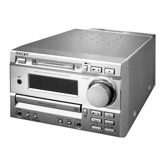
SECTION 2 GENERAL Front Panel LOCATION OF PARTS AND CONTROLS 1 1/u (power) switch 2 MD slot 3 6 (Eject) (MD) button 4 MD indicator 5 (P (MD) button 6 p (MD) button 7 VOLUME (CD) knob 8 (P (CD) button 9 p (CD) button 10 TUNER/BAND button 11 FUNCTION button... - Page 17 This section is extracted from instruction manual.
-
Page 19: Disassembly
SECTION 3 DISASSEMBLY Note: Follow the disassembly procedure in the numerical order given. Case Front panel Main board and Power transformer Back panel (Page 19) (Page 20) (Page 21) (Page 20) CD base unit section Optical pick-up (CD) (Page 22) (Page 22) BD (CD) board Sled motor (M102) -
Page 20: Front Panel
3-2. FRONT PANEL 8 Screw 5 Screw (BVTT 3x6) (BVTT 3x10) 0 MD mechanism block 7 Front panel block 9 Screw (Two claws) (BVTT 3x6) 1 Flat type wire 2 Flat type wire (31 core) (25 core) Claw 3 Ground wire (Black) 6 Screw (BVTT 3x6) Claw... -
Page 21: Main Board And Power Transformer
3-4. MAIN BOARD AND POWER TRANSFORMER 4 Connector (2P) 5 Connector (2P) 3 Connector (4P) !™ Power transformer 7 Screw (BVTP 3x6) 6 Connector (Amp board, CN801) (Take note of the claw) Amp board (CN801) 8 Screw (BVTP 3x6) 0 Connector (3P) SP board Power board 2 Flat type wire... -
Page 22: Tray, Gear And Cam
3-6. TRAY, GEAR AND CAM 4 Belt (CDM55) 5 Bushing 6 Pulley (LDG) 8 Gear (B) 9 Gear (A) 7 Roller 0 Cam (CDM55) 2 Push the claw in tne direction of arrow C . 1 Pull out the tray in the arrow direction A , and release the lock while pressing this claw in the arrow direction B . -
Page 23: Bd (Cd) Board, Spindle Motor (M101) And Sled Motor (M102)
3-9. BD (CD) BOARD, SPINDLE MOTOR (M101) AND SLED MOTOR (M102) 6 Gear (M) 4 Two screws (P 2x3) 8 Two Insulators (BU) !¡ Spindle motor (M101) 2 Remove the four solders. 0 Sled shaft 7 Flatness gear (P) M101 IC102 M102 5 Sled motor... -
Page 24: Slider (Cam)
3-11. SLIDER (CAM) 6 Slider (CAM) • Note for installation of Slider (CAM) Set the shaft of Cam gear to be at the position in the figure. 2 Bracket (GUIDE L) 1 Two screws (BTP 2.6x6) Set the shaft of Lever (O/C) to 3 Leaf spring be at the position in the figure. -
Page 25: Over Write Head
3-13. OVER WRITE HEAD 3-14. OPTICAL PICK-UP OF MD (KMS-260B/J1N) Note: Turn the optical pick-up 2 Screw (P 1.7x6) 5 Optical pick-up (for MD) inside out, and pull out the flexible board. 3 Over write head (HR901) 4 Flexible board 1 Flexible board 1 Screw (B 2x8) 2 Leaf spring (SHAFT) -
Page 26: Test Mode
SECTION 4 TEST MODE Note 1: About “R” As this unit has only a few buttons, some operations require the use of remote commander (RM-SJ373/provided with unit: 1-418-554-11) buttons. These operations are indicated as “R” in this manual. Example: MENU/NO “R” ...Press the MENU/NO button of the remote commander. 4-1. - Page 27 4-5. SELECTING THE TEST MODE There are 31 types of test modes as shown below. The groups can be switched by pressing the =0/MD/CD/TUNING – button or )+/MD/CD/TUNING + button. After selecting the group to be used, press the ENTER/YES “R” button. After setting a certain group, pressing the =0/MD/CD/TUNING –...
- Page 28 4-5-1. Operating the Continuous Playback Mode 1. Entering the continuous playback mode 1 Set the disc in the unit. (Whichever recordable discs or discs for playback only are available.) 2 Press the =0/MD/CD/TUNING – button or )+/MD/CD/TUNING + button and display “CPLAY MODE”. 3 Press the ENTER/YES “R”...
- Page 29 4-6. FUNCTIONS OF OTHER BUTTONS Contents Function ^ (MD) Sets continuous playback when pressed in the STOP state. When pressed during continuous playback, the tracking servo turns ON/OFF. Stops continuous playback and continuous recording. p (MD) The sled moves to the outer circumference only when this is pressed. )+/MD/CD/TUNING + The sled moves to the inner circumference only when this is pressed.
- Page 30 MEANINGS OF OTHER DISPLAYS Contents Display When Lit When Off During continuous playback (CLV: ON) ( (MD) * STOP (CLV: OFF) Tracking servo OFF P (MD) * Tracking servo ON Recording mode ON r REC * Recording mode OFF CLV low speed mode CLV normal mode SYNC ABCD adjustment completed...
-
Page 31: Electrical Adjustments
SECTION 5 ELECTRICAL ADJUSTMENTS MD SECTION 5-1. PARTS REPLACEMENT AND ADJUSTMENT • Check and adjust the MDM and MBU as follows. The procedure changes according to the part replaced • Abbreviation : Optical pick-up OWH: Overwrite head • Temperature compensation offset check •... - Page 32 5-2. PRECAUTIONS FOR CHECKING LASER DIODE 4) Use the following tools and measuring devices. • Check Disc (MD) TDYS-1 EMISSINON (Parts No. 4-963-646-01) To check the emission of the laser diode during adjustments, never • Test Disk (MDW-74/AU-1) (Parts No. 8-892-341-41) view directly from the top as this may lose your eye-sight.
- Page 33 5-6. CHECKS PRIOR TO REPAIRS 5. Press the MENU/NO “R” button and display “LDPWR CHECK” and stop the laser emission. These checks are performed before replacing parts according to (The MENU/NO “R” button is effective at all times to stop the “approximate specifications”...
- Page 34 5-6-4. Focus Bias Check 9. Press the ENTER/YES “R” button display “EFB = MO-P”. Then, the optical pick-up moves to the pit area automatically Change the focus bias and check the focus tolerance amount. and servo is imposed. Checking Procedure : 10.
- Page 35 5-9. TEMPERATURE COMPENSATION OFFSET 8. “C1 = AD = ” will be displayed. 9. Check that the C1 error becomes below 80 and the AD error ADJUTMENT below 2. Save the temperature data at that time in the non-volatile memory 10.
- Page 36 5-11. TRAVERSE ADJUSTMENT 5. Then “LD 7.0 mW $ ” will be displayed. 6. Press the =0/MD/CD/TUNING – button or )+/ Connection : MD/CD/TUNING + button so that the reading of the laser power Oscilloscope meter becomes 6.9 to 7.1 mW, press the ENTER/YES “R” but- ton and save it.
- Page 37 9. Press the ENTER/YES “R” button, and save the adjustment 5-12. FOCUS BIAS ADJUSTMENT results in the non-volatile memory. (“EFB = SAVE” will be Adjusting Procedure : displayed for a moment.) 1. Load a test disk (MDW-74/AU-1). 10. “EFB = MO-P”.
- Page 38 5-13. ERROR RATE CHECK 5-15. AUTO GAIN CONTROL OUTPUT LEVEL 5-13-1. CD Error Rate Check ADJUSTMENT Checking Procedure : Be sure to perform this adjustment when the pickup is replaced. 1. Load a check disc (MD) TDYS-1. If the adjustment results becomes “Adjust NG!”, the pickup may be 2.
- Page 39 Note: Clear RF signal waveform means that the shape “ ” can be 5-15. ADJUSTING POINTS AND CONNECTING POINTS CD SECTION clearly distinguished at the center of the waveform. [BD (MD) BOARD] (SIDE A) Note: RF signal waveform 1. CD Block is basically constructed to operate without adjustment. VOLT/DIV : 200mV CN101 TIME/DIV : 500ns...
-
Page 40: Diagrams
HCD-MD373 SECTION 6 DIAGRAMS 6-1. CIRCUIT BOARDS LOCATION Amp board Power board SP board MD digital board Tuner unit TUNER UNIT is supplied as the assembled block. Panel board Main board SW board BD (MD) board BD (CD) board Loading board... -
Page 41: Block Diagrams
HCD-MD373 6-2. BLOCK DIAGRAMS – BD (CD) SECTION – OPTICAL PICK-UP BLOCK (KSS-213BA/NP) IC101 XTA1 DETECTOR DIGITAL SERVO X101 TIMING IC103 DIGITAL SIGNAL PROCESSOR LOGIC 16.9344MHz RF AMP ERROR STAO CORRECTOR RF EQ RF AC DIGITAL D OUT SUMMING DOUT... -
Page 42: Bd (Md) Section (1/2)
HCD-MD373 – BD (MD) SECTION (1/2) – DIGITAL SERVO SIGNAL PROCESSOR, DIGITAL SIGNAL PROCESSOR EFM/ACIRC ENCODER/DECODER, SHOCK-PROOF MEMORY CONTROLLER, ATRAC ENCODER/DECODER IC121 OVER WRITE HEAD DRIVE IC181 HR901 OVER WRITE • DIN0 HEAD DIN0 • R-ch is omitted HEAD •... -
Page 43: Bd (Md) Section (2/2)
HCD-MD373 – BD (MD) SECTION (2/2) – A/D,D/A CONVERTER IC201 MD REC-L DATAO VINL1 (AD IN L) VINR1 R-CH MD-L VOUTL (DATA OUT L) VOUTR R-CH MAIN SECTION ADDT MD LEVEL L (Page 44) MD LEVEL R LRCK DADT DATAI... -
Page 44: Main Section
HCD-MD373 – MAIN SECTION – MUTE SW MUTE SW Q551 Q841 RY881 1 POWER AMP IC801 R-CH TUNER UNIT – TM881 ANTENNA DBFB SW DBFB DET RELAY DRIVE SPEAKER Q301 D881 Q881 STEREO – TUNED PROTECT SW OVER LOAD DET R-CH Q872–873... - Page 45 HCD-MD373 WAVEFORMS – BD (MD) (1/2) SECTION – – MAIN (3/3) SECTION – THIS NOTE IS COMMON FOR PRINTED WIRING – BD ( CD) SECTION – BOARDS AND SCHEMATIC DIAGRAMS. (In addition to this, the necessary note is printed in each block.) 0.46Vp-p...
-
Page 46: Printed Wiring Board - Bd (Cd) Section
HCD-MD373 6-3. PRINTED WIRING BOARD – BD (CD) SECTION – • See page 40 for Circuit Boards Location. (VC) (RF) (AGC CON) MAIN BOARD (FE) (TE) (TEI) (Page 52) -
Page 47: Schematic Diagram - Bd (Cd) Section
HCD-MD373 6-4. SCHEMATIC DIAGRAM – BD (CD) SECTION – • See page 45 for Waveforms. • See page 67 for IC Block Diagrams. • See page 69 for IC Pin Functions. (RF) (VC) (TE) (FE) AGC CON (TE1) (FEI) MAIN BOARD... -
Page 48: Printed Wiring Board - Bd (Md) Section
HCD-MD373 6-5. PRINTED WIRING BOARD – BD (MD) SECTION – • See page 40 for Circuit Boards Location. • Semiconductor Location • Semiconductor Location Ref. No. Location Ref. No. Location IC101 D101 IC121 (Page 57) (Page 57) D181 IC124 D183... -
Page 49: Schematic Diagram - Bd (Md) Section - (1/2)
HCD-MD373 6-6. SCHEMATIC DIAGRAM – BD (MD) SECTION (1/2) – • See page 45 for Waveforms. • See page 65 for IC Block Diagrams. • See page 71 for IC Pin Functions. (Page 50) (Page 50) (Page 50) (Page 50) -
Page 50: Schematic Diagram - Bd (Md) Section - (2/2)
HCD-MD373 6-7. SCHEMATIC DIAGRAM – BD (MD) SECTION (2/2) – • See page 45 for Waveforms. • See page 48 for Printed Wiring Board. • See page 66 for IC Block Diagrams. (Page 49) (Page 49) (Page 49) (Page 49) -
Page 51: Schematic Diagram - Sp Section
HCD-MD373 6-8. SCHEMATIC DIAGRAM – SP SECTION – 6-9. PRINTED WIRING BOARD – SP SECTION – • See page 40 for Circuit Boards Location. (Page 58) (Page 59) (Page 53) (Page 52) -
Page 52: Printed Wiring Board - Main Section
HCD-MD373 6-10. PRINTED WIRING BOARD – MAIN SECTION – • See page 40 for Circuit Boards Location. • Semiconductor Location Ref. No. Location D171 D301 C-10 D302 D901 (Page 57) (Page 46) D911 D912 D913 (Page 51) D914 D921 D922... -
Page 53: Schematic Diagram - Main Section - (1/3)
HCD-MD373 6-11. SCHEMATIC DIAGRAM – MAIN SECTION (1/3) – • See page 68 for IC Block Diagrams. (Page 51) (Page 55) (Page 54) (Page 54) (Page 55) (Page 54) -
Page 54: Schematic Diagram - Main Section - (2/3)
HCD-MD373 6-12. SCHEMATIC DIAGRAM – MAIN SECTION (2/3) – • See page 52 for Printed Wiring Board. • See page 68 for IC Block Diagrams. (Page 53) (Page 53) (Page 53) (Page 62) (Page 56) (Page 55) (Page 55) (Page 55) -
Page 55: Schematic Diagram - Main Section - (3/3)
HCD-MD373 6-13. SCHEMATIC DIAGRAM – MAIN SECTION (3/3) – • See page 45 for Waveforms. • See page 52 for Printed Wiring Board. • See page 68 for IC Block Diagrams. • See page 75 for IC Pin Functions. (Page... -
Page 56: Schematic Diagram - Md Digital Section
HCD-MD373 6-14. SCHEMATIC DIAGRAM – MD DIGITAL SECTION – • See page 45 for Waveforms. • See page 67 for IC Block Diagrams. (Page 54) (Page 64) (Page 50) (Page 50) -
Page 57: Printed Wiring Board - Md Digital Section
HCD-MD373 6-15. PRINTED WIRING BOARD – MD DIGITAL SECTION – • See page 40 for Circuit Boards Location. (Page 64) (Page 48) (Page 48) (Page 52) -
Page 58: Schematic Diagram - Amp Section
HCD-MD373 6-16. SCHEMATIC DIAGRAM – AMP SECTION – (Page 62) (Page 51) -
Page 59: Printed Wiring Board - Amp Section
HCD-MD373 6-17. PRINTED WIRING BOARD – AMP SECTION – • See page 40 for Circuit Boards Location. (Page 51) (Page 63) -
Page 60: Schematic Diagram - Panel Section
HCD-MD373 6-18. SCHEMATIC DIAGRAM – PANEL SECTION – (Page 55) -
Page 61: Printed Wiring Board - Panel Section
HCD-MD373 6-19. PRINTED WIRING BOARD – PANEL SECTION – • See page 40 for Circuit Boards Location. • Semiconductor Location Ref. No. Location D602 D603 D604 D605 D606 D607 D608 D609 IC601 IC602 Q601 Q602 Q604 Q605 Q606 Q607 Q608... -
Page 62: Schematic Diagram - Power Section
HCD-MD373 6-20. SCHEMATIC DIAGRAM – POWER SECTION – (Page 58) (Page 54) -
Page 63: Printed Wiring Board - Power Section
HCD-MD373 6-21. PRINTED WIRING BOARD – POWER SECTION – • See page 40 for Circuit Boards Location. • Semiconductor Location Ref. No. Location (Page 52) D971 D972 D973 D974 D975 D976 D977 D978 D979 D980 D981 D982 D985 D986 D987... -
Page 64: Schematic Diagram - Bd Switch Section
HCD-MD373 6-22. SCHEMATIC DIAGRAM – BD SWITCH SECTION – 6-24. SCHEMATIC DIAGRAM – LOADING SECTION – LOADING SWITCH CLOSE MD DIGITAL BOARD OPEN (Page 56) LOAD + MAIN BOARD LOAD – (3/3) M103 (Page 55) LOADING MOTOR 6-23. PRINTED WIRING BOARD – BD SWITCH SECTION –... -
Page 65: Ic Block Diagrams
6-26. IC BLOCK DIAGRAMS • BD (MD) Board (1/2) IC101 CXA2523AR 43 42 USROP – RF AGC – USRC RFA1 BPF3T RFA2 PEAK3T – HLPT –1 – – –2 – CFST PTGR TEMP PEAK – –2 – 36 BOTM BOTTOM –... - Page 66 IC152 BH6511FS-E2 INTERFACE INTERFACE CHARGE PREDRIVE PREDRIVE PUMP. PREDRIVE PREDRIVE INTERFACE INTERFACE • BD (MD) Board (2/2) IC121 CXD2654R 100 99 98 97 96 95 94 93 92 91 90 89 88 87 86 85 84 83 82 81 80 79 78 77 76 SPINDLE GENERATOR SERVO...
- Page 67 • BD (CD) Board IC101 CXD2587Q ERROR ASYMMETRY DIGITAL DIGITAL CORRECTOR CORRECTION LRCK OPERATIONAL AMPLIFIER PCMD INTERFACE DEMODULATOR ANALOG SWITCH CONVERTER EMPH XVDD CLOCK XTSL GENERATOR XTAI TIMING TES1 LOGIC XTAO TEST XVSS SERVO DSP PWM GENERATOR AVDD1 FRDR FOCUS FOCUS PWM AOUT1 SERVO...
- Page 68 • MAIN Board (3/3) IC302 MC14052B IC171 LB1641 T.S.D O.C.P 2XCOM MOTOR MOTOR DRIVE DRIVE XCOM FWD/REV/STOP CONTROL LOGIC • MAIN Board (2/3) • MAIN Board (1/3) IC301 M62428AFP IC931 M62016L DARA MICROCOMPUTER INTERFACE INTERRUPT SIGNAL DVDD LATCH – GENERATING BLOCK AVDD DGND RESET SIGNAL...
-
Page 69: Ic Pin Functions
6-27. IC PIN FUNCTIONS • IC101 DIGITAL SIGNAL PROCESSOR (CXD2587Q) (BD(CD) board) Pin No. Pin Name Function SQSO Sub-Q 80-bit and PCM peak level data output (CD text data output) SQCK Clock input for SQSO read-out XRST System reset “L” : reset SYSM Muting input “H”... - Page 70 Pin No. Pin Name Function Tracking error signal input Center servo analog input RFDC RF signal input Test pin (Not used) ADIO — Analog ground AVSS0 Stabilized current input for operational amplifiers IGEN — Analog power supply AVDD0 EFM full swing output ASYO EFM asymmetry comparate voltage input ASYI...
- Page 71 • IC101 RF Amplifier (CXA2523AR) (BD(MD) board) Pin No. Pin Name Function I-V converted RF signal I input I-V converted RF signal J input Middle point voltage (+1.5V) generation output 4 to 9 A to F Signal input from the optical pick-up detector Light amount monitor input Laser APC output APCREF...
- Page 72 • IC121 Digital Signal Processor, Digital Servo Signal Processor, EFM/ACIRC Encoder/Decoder, Shock-proof Memory Controller, ATRAC Encoder/Decoder, 2M Bit DRAM (CXD2654R) (BD (MD) board) Pin No. Pin Name Function FOK signal output to the system control (monitor output) MNT0 (FOK) “H” is output when focus is on MNT1 (SHCK) Track jump detection signal output to the system control (monitor output) MNT2 (XBUSY)
- Page 73 Pin No. Pin Name Function Data input/output for DRAM 50, 51 D2, D3 MVCI Clock input from an external VCO (Fixed at “L”) I (S) ASYO Playback EFM duplex signal output ASYI I (A) Playback EFM comparator slice level input AVDD —...
- Page 74 Pin No. Pin Name Function Tracking servo drive PWM output (+) TFDR — +3V power supply (Digital) DVDD Focus servo drive PWM output (+) FFDR Focus servo drive PWM output (–) FRDR 176.4 kHz clock signal output (X’tal) (Not used) Sled servo drive PWM output (–) SRDR Sled servo drive PWM output (+)
- Page 75 • IC501 MASTER CONTROL (M30620ECFP-A21) (MAIN board) Pin Name Function Pin No. STK-POWER Power amp ON/OFF signal output Power ON/OFF signal output (Not used) F-RY Front speaker relay control output R-RY Rear speaker relay control output (Not used) CD-POWER CD power on signal output TA-MUTE Line mute ON/OFF signal output DBFB-H...
- Page 76 Pin Name Function Pin No. STEREO Stereo signal input from the tuner TUNED Tuned signal input from the tuner ST-CE Tuner chip enable output ST-DOUT Tuner data output ST-DIN Tuner data input ST-CLK Tuned clock output SENS BD Condition signal input HDLD Mode hold signal output CD-LAT...
-
Page 77: Exploded Views
X-4951-763-3 PANEL ASSY, FRONT A-4426-083-A MD DIGITAL BOARD, COMPLETE 1-773-212-11 WIRE (FLAT TYPE) (25 CORE) 4-930-336-71 FOOT (FELT) 1-791-211-11 WIRE (FLAT TYPE) (23 CORE) 4-962-708-61 EMBLEM (4-A), SONY 1-777-240-11 WIRE (FLAT TYPE) (21 CORE) 4-216-729-41 LID (CARTRIDGE) 4-221-097-01 BRACKET (MDM) 4-223-771-01 SPRING (LID) -
Page 78: Chassis Section
7-2. CHASSIS SECTION not supplied T900 T901 CDM55A-5SBD32 not supplied not supplied UK,HK EXCEPT AR,AUS The components identified by mark ! or dotted line with mark ! are critical for safety. Replace only with part number specified. Ref. No. Part No. Description Remark Ref. -
Page 79: Md Mechanism Section (Mdm-5A)
7-3. MD MECHANISM DECK (MDM-5A) not supplied M903 MBU-5A Ref. No. Part No. Description Remark Ref. No. Part No. Description Remark * 101 1-668-111-11 SW BOARD 4-996-229-01 SPRING (HEAD LEVER), TORSION * 102 4-996-217-01 CHASSIS 4-996-212-01 LEVER (LIMITTER) 4-996-223-01 INSULATOR (F) 4-996-213-01 SPRING (LIMITTER), TORSION * 104 4-996-218-01 BRACKET (GUIDE R) -
Page 80: Md Base Unit Section (Mbu-5A)
7-4. MD BASE UNIT (MBU-5A) HR901 not supplied not supplied not supplied M901 S102 M902 The components identified by mark ! or dotted line with mark ! are critical for safety. Replace only with part number specified. Ref. No. Part No. Description Remark Ref. -
Page 81: Cd Mechanism Section (Cdm55A-5Sbd32)
Ver 1.1 2001.06 7-5. CD MECHANISM DECK (CDM55A-5SBD32) (CDM identification: cleam colored chassis) not supplied not supplied M103 BU-5SBD32 not supplied Ref. No. Part No. Description Remark Ref. No. Part No. Description Remark 4-925-315-31 DAMPER 4-221-816-01 BEL T (CDM55) 1-674-336-11 LOADING BOARD 4-221-916-01 BUSHING 4-220-231-01 TRA Y (CDM) A-4672-773-A... -
Page 82: Cd Base Unit Section (Bu-5Sbd32)
Ver 1.1 2001.06 7-6. CD BASE UNIT (BU-5SBD32) (BU identification: black plastic turntable with magnet) M102 M101 (including r C) The components identified by mark ! or dotted line with mark ! are critical for safety Replace only with part number specified. Ref. -
Page 83: Cd Mechanism Section (Cdm55C-5Bd32)
Ver 1.1 2001.06 7-7. CD MECHANISM DECK (CDM55C-5BD32) (CDM identification: black colored holder (AT) (319), pulley (313) with magnet) M103 BU-5BD32 not supplied Ref. No. Part No. Description Remark Ref. No. Part No. Description Remark 4-925-315-41 DAMPER 4-221-816-11 BELT (CDM55) 1-674-336-11 LOADING BOARD 1-452-925-21 MAGNET ASSY 4-224-894-11 TRAY (CDM55D) -
Page 84: Cd Base Unit Section (Bu-5Bd32)
Ver 1.1 2001.06 7-8. CD BASE UNIT (BU-5BD32) (BU identification: metal turntable without magnet) M102 M101 (including r C) The components identified by mark ! or dotted line with mark ! are critical for safety Replace only with part number specified. Ref. -
Page 85: Electrical Parts List
SECTION 8 ELECTRICAL PARTS LIST Note: • Due to standardization, replacements in the parts list • CAPACITORS The components identified by uF : µ F may be different from the parts specified in the mark ! or dotted line with mark •... - Page 86 BD (CD) Ref. No. Part No. Description Remark Ref. No. Part No. Description Remark R853 1-249-437-11 CARBON 1/4W C162 1-126-205-11 ELECT CHIP 47uF 6.3V R854 1-249-437-11 CARBON 1/4W C163 1-126-206-11 ELECT CHIP 100uF 6.3V R855 1-249-417-11 CARBON 1/4W F R856 1-249-437-11 CARBON 1/4W C165...
- Page 87 BD (CD) BD (MD) Ref. No. Part No. Description Remark Ref. No. Part No. Description Remark C136 1-126-206-11 ELECT CHIP 100uF 6.3V R158 1-216-111-00 METAL CHIP 390K 1/10W C142 1-163-251-11 CERAMIC CHIP 100PF R159 1-216-101-00 METAL CHIP 150K 1/10W C143 1-163-251-11 CERAMIC CHIP 100PF C144...
- Page 88 BD (MD) MD DIGITAL Ref. No. Part No. Description Remark Ref. No. Part No. Description Remark L106 1-414-813-11 FERRITE R149 1-216-073-00 METAL CHIP 1/10W R150 1-216-295-91 SHORT L121 1-414-813-11 FERRITE R151 1-216-073-00 METAL CHIP 1/10W L122 1-414-813-11 FERRITE R152 1-216-073-00 METAL CHIP 1/10W L151 1-412-029-11 INDUCTOR CHIP 10uH...
- Page 89 LOADING MAIN MD DIGITAL Ref. No. Part No. Description Remark Ref. No. Part No. Description Remark C358 1-163-251-11 CERAMIC CHIP 100PF R385 1-216-073-00 METAL CHIP 1/10W C359 1-163-251-11 CERAMIC CHIP 100PF R386 1-216-073-00 METAL CHIP 1/10W C360 1-163-251-11 CERAMIC CHIP 100PF R391 1-216-073-00 METAL CHIP...
- Page 90 MAIN Ref. No. Part No. Description Remark Ref. No. Part No. Description Remark C407 1-164-031-11 CERAMIC 33PF C161 1-126-933-11 ELECT 100uF AEP,UK C501 1-164-025-51 CERAMIC 18PF C166 1-162-282-31 CERAMIC 100PF C502 1-164-025-51 CERAMIC 18PF C167 1-162-294-31 CERAMIC 0.001uF C503 1-162-306-11 CERAMIC 0.01uF C171 1-164-159-11 CERAMIC...
- Page 91 MAIN Ref. No. Part No. Description Remark Ref. No. Part No. Description Remark D922 8-719-911-19 DIODE 1SS133T-72 < RESISTOR > D923 8-719-911-19 DIODE 1SS133T-72 R101 1-249-441-11 CARBON 100K 1/4W D924 8-719-911-19 DIODE 1SS133T-72 R102 1-249-417-11 CARBON 1/4W F D941 8-719-911-19 DIODE 1SS133T-72 R103 1-249-429-11 CARBON 1/4W...
- Page 92 MAIN Ref. No. Part No. Description Remark Ref. No. Part No. Description Remark R549 1-247-807-31 CARBON 1/4W R402 1-249-417-11 CARBON 1/4W F R550 1-247-807-31 CARBON 1/4W (AEP,UK) R551 1-249-437-11 CARBON 1/4W R552 1-249-429-11 CARBON 1/4W R403 1-249-429-11 CARBON 1/4W R553 1-249-417-11 CARBON 1/4W F (AEP,UK)
- Page 93 PANEL Ref. No. Part No. Description Remark Ref. No. Part No. Description Remark < IC > A-4426-073-A PANEL BOARD, COMPLETE ********************** IC601 8-759-297-23 IC M66004M8FP IC602 8-759-459-85 IC NJL63H400A 1-690-880-31 LEAD (WITH CONNECTOR) 4-221-103-01 HOLDER (FL) < JACK > < CAPACITOR > J601 1-764-106-21 JACK (PHONES) J602...
- Page 94 PANEL POWER Ref. No. Part No. Description Remark Ref. No. Part No. Description Remark R651 1-249-429-11 CARBON 1/4W * CN993 1-564-519-11 PLUG, CONNECTOR 4P R652 1-249-435-11 CARBON 1/4W * CN994 1-770-730-11 CONNECTOR, BOARD TO BOARD 11P R681 1-162-600-11 CERAMIC 0.0047uF 30% R682 1-249-441-11 CARBON 100K...
- Page 95 POWER Ref. No. Part No. Description Remark Ref. No. Part No. Description Remark < SWITCH > R895 1-260-076-11 CARBON 1/2W ! R896 1-215-891-11 METAL OXIDE ! S991 1-571-309-11 SWITCH (VOLTAGE SELESTOR) (AEP,UK) (AUS,AR,HK,JE,MY,SP,KR,CH) ! R896 1-216-454-11 METAL OXIDE (AUS,AR,HK,JE,MY,SP,KR,CH) < TRANSFORMER > <...
- Page 96 HCD-MD373 Ver 1.1 2001.06 Ref. No. Part No. Description Remark ************* HARDWARE LIST ************* 7-685-647-79 SCREW +BVTP 3X10 TYPE2 TT(B) 7-685-650-91 SCREW +BVTP 3X16 TYPE2 TT(B) 7-685-871-01 SCREW +BVTT 3X6 (S) 7-685-533-19 SCREW +BTP 2.6X6 TYPE2 N-S 7-627-852-08 SCREW,PRECISION +P 1.7X2.5...
- Page 97 HCD-MD373 MEMO...
- Page 98 HCD-MD373 REVISION HISTORY Clicking the version allows you to jump to the revised page. Also, clicking the version at the upper right on the revised page allows you to jump to the next revised page. Ver. Date Description of Revision 2001.06...