Table of Contents
Advertisement
SERVICE MANUAL
Ver 1.1 2001. 08
• This set is the Amplifier, CD player,
MD Deck and Tuner section in
DHC-MD555.
Manufactured under license from Dolby Laboratories
Licensing Corporation.
"DOLBY" the double-D symbol a "AC-3" and "PRO
LOGIC" are trademarks of Dolby Laboratories
Licensing Corporation.
Sony Corporation
9-922-976-12
2001H1600-1
Home Audio Company
© 2001.8
Shinagawa Tec Service Manual Production Group
HCD-MD555
Model Name Using Similar Mechanism
CD Section
CD Mechanism Type
Optical Pick-up Type
Model Name Using Similar Mechanism
MD Mechanism Type
MD Section
Base Unit Type
Optical Pick-up Type
SPECIFICATIONS
MINI Hi-Fi COMPONENT SYSTEM
US Model
AEP Model
UK Model
E Model
Tourist Model
NEW
CDM53-K1BD33
KSM-213BFN/C2NP
NEW
MDM-C1E
MBU-C1E
KSM-260A/J1N
— Continued on next page —
Advertisement
Table of Contents

Related Manuals for Sony HCD-MD555


Summary of Contents for Sony HCD-MD555
- Page 1 HCD-MD555 SERVICE MANUAL US Model AEP Model Ver 1.1 2001. 08 UK Model E Model Tourist Model • This set is the Amplifier, CD player, MD Deck and Tuner section in DHC-MD555. Manufactured under license from Dolby Laboratories Model Name Using Similar Mechanism Licensing Corporation.
- Page 2 COMPONENTS IDENTIFIED BY MARK ! OR DOTTED LINE WITH MARK ! ON THE SCHEMATIC DIAGRAMS AND IN THE PARTS LIST ARE CRITICAL TO SAFE OPERATION. REPLACE THESE COMPONENTS WITH SONY PARTS WHOSE PART NUMBERS APPEAR AS SHOWN IN THIS MANUAL OR IN SUPPLEMENTS PUBLISHED BY SONY.
- Page 3 0.15 µ F 1.5k Ω (0.75V) MODEL IDENTIFICATION – BACK PANEL – Earth Ground HCD-MD555 MODEL NO. COMPACT DISC DECK RECEIVER SERIAL Fig. A. Using an AC voltmeter to check AC leakage. MADE IN JAPAN AC: 230V ~ 50/60Hz 90W: AEP, UK model AC: 110 –...
-
Page 4: Table Of Contents
TABLE OF CONTENTS 1. SELF-DIAGNOSIS FUNCTION 7. DIAGRAMS ·································· 5 7-1. Block Diagrams ································································ 53 • MD Section ···································································· 53 2. SERVICE NOTE ······························································· 8 • CD Section ····································································· 55 • Audio Section ································································ 57 3. GENERAL ········································································ 12 • Power Section ································································ 59 7-2. -
Page 5: Self-Diagnosis Function
8. You can exit the error history mode by pressing the MENU/NO button. The message “ERR DP MODE” is displayed. 9. You can exit the test mode by pressing the REPEAT . Then the HCD-MD555 enters the standby state, the disc is ejected, and the display exits the test mode. - Page 6 DISPLAYING CONTENTS OF THE ERROR HISTORY 1. Select the desired item of history using the MULTI JOG dial. 2. Press the MD WALKMAN SYNC button to display the desired content of the selected error item. 3. Press the MD WALKMAN SYNC button again to return to the history item display screen. Table 1 shows error history items and the contents.
- Page 7 (Note 2) NO DISC code in the order of occurrence CD SECTION ∗∗ ∗∗ ∗∗ ∗∗ OPERATING THE DISPLAYED HISTORIES When the three buttons of ENTER/YES , PRESET EQ , and CD3 are pressed simultaneously, and the mechanical error count and the count of “NO DISC”...
-
Page 8: Service Note
SECTION 2 SERVICE NOTE CD-TEXT TEST DISC This unit is able to display the test data (character information) written in the CD on its fluorescent indicator tube. The CD-TEXT TEST DISC (TGCS-313:4-989-366-01) is used for checking the display. To check, perform the following procedure. Checking Method: Turn ON the power, set the disc on a tray, and chuck the disc. - Page 9 Table 2: CD-TEXT TEST DISC Recorded Data Contents and Display (TRACKS NO. 33 to 99) (In this unit, some special characters cannot be displayed. This is no a fault.) TRACK Recorded contents Display 100Hz/0dB/R* 1kHz/0dB/R* Same as the values shown in the left column. ...
- Page 10 IOP DATA RECORDING AND DISPLAY WHEN THE OPTICAL PICKUP AND NON-VOLATILE MEMORY (BD (MD) BOARD IC171) IS REPLACED The IOP value that is indicated on the optical pickup unit can be saved in the non-volatile memory. By saving the IOP value saved in the non- volatile memory, it is no more necessary to read the IOP value on the optical pickup unit.
- Page 11 CHECK BEFORE STARTING PARTS REPLACEMENT AND ADJUSTMENT Cause of defect can be approximately located by performing the following checks before starting repair work. For the detailed procedure, refer to “SECTION 6 ELECTRICAL ADJUSTMENTS”. Criterion of judgement Countermeasure when result of judgement (If the value does not satisfy the following is defective specification value, it is judged as defective.)
-
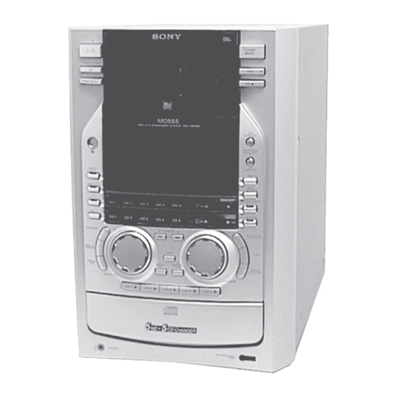
Page 12: General
SECTION 3 GENERAL #¡ #º @ª @• @¶ @§ !º @∞ !¡ @¢ !™ @£ !£ @™ !¢ @¡ @º !∞ !§ !ª !• !¶ 1 TUNER/BAND button !§ CLEAR button 2 DBFB button !¶ ENTER/YES button 3 MD6 button !•... - Page 13 This section is extracted from instruction manual. — 13 —...
- Page 14 — 14 —...
- Page 15 — 15 —...
- Page 16 — 16 —...
- Page 17 — 17 —...
- Page 18 — 18 —...
- Page 19 — 19 —...
- Page 20 — 20 —...
- Page 21 — 21 —...
- Page 22 — 22 —...
- Page 23 — 23 —...
- Page 24 — 24 —...
-
Page 25: Disassembly
SECTION 4 DISASSEMBLY Note : Follow the disassembly procedure in the numerical order given. 4-1. BACK PANEL • Remove the upper cover first. 5 Three connectors 6 Back panel 2 Cover (Back) 3 Ten screws (+BV 3 × 8) 4 Seven screws (+BV 3 ×... -
Page 26: Sp Board, Amp Board, Reg Board
4-3. SP BOARD, AMP BOARD, REG BOARD, TRANS-D BOARD (JE, HK, SP, MY MODEL) Abbreviation 9 Four screws !º Heat sink 2 Two screws HK : Hong Kong (+BV 3 × 12) (+BV 3 × 8) SP : Singapore MY : Malaysia JE : Tourist 3 SP board 8 AMP board... -
Page 27: Power Key Board, Led Board, Panel Board
4-5. POWER KEY BOARD, LED BOARD, PANEL BOARD 1 Two screws 6 POWER KEY board (+BV 3 × 8) 8 LED board 2 Chassis (MD) 5 Two screws (+BVTP 2.6 × 8) 9 Two screws (+BVTP 2.6 × 8) 7 Screw (+BVTP 2.6 ×... -
Page 28: Cd Mechanism (Cdm53-K1Bd33)
4-7. CD MECHANISM (CDM53-K1BD33) 2 Two screws (+BV 3 × 8) 1 Two screws (+BV 3 × 8) 3 CD mechanism (CDM53-K1BD33) Chassis — 28 —... -
Page 29: Escutcheon, Chassis (Top)
4-8. ESCUTCHEON, CHASSIS (TOP) 5 Two screws (+BVTT 2.6 × 5) 7 Screw (+BVTT 2.6 × 5) 6 Cover (FFC) 9 Bracket (To assemble the bracket, refer to the following note.) !º Two screws (+P 2 × 5) !™ Chassis (TOP) 4 Flat type wire (13 core) 8 Lever (S) assy... -
Page 30: Chassis (Elevator) New
4-9. CHASSIS (ELEVATOR) NEW 1 Chassis (Elevator) NEW assy 4-10. MOTOR (HEAD) ASSY (M905), HEAD RELAY BOARD 7 Remove soldering of the motor. 8 HEAD RELAY board 1 Connector 3 Screw (+BVTT 2.6 × 5) 6 Motor (Head) assy (M905) 2 Belt A Remove the motor assy in the direction of the arrow B . -
Page 31: Md Base Unit (Mbu-C1E)
4-11. MD BASE UNIT (MBU-C1E) 2 Four step screws 3 MD base unit (MBU-C1E) Note: Remove the MD base unit while 1 Connector being careful of the over-write head. Over-write head 4-12. BD BOARD 4 Two screws (+P 1.7 × 2.2) 6 OP translation flexible pc board 2 Connector... -
Page 32: Over Light Head (Hr901)
4-13. OVER LIGHT HEAD (HR901) 1 Screw (+P1.7 × 2.5) 2 Over light head (HR901) 4-14. MD OPTICAL PICK-UP BLOCK (KMS-260A/J1N) 4 Optical pick-up block (KMS-260A/JIN) Remove the optical pickup block in the direction of the arrow. 1 Screw (M 1.7 × 1.4) 2 Stopper 3 Shaft (MAIN) —... -
Page 33: Cd Optical Pick-Up Block (Kss-213Ba/F-Np)
4-15. CD OPTICAL PICK-UP BLOCK (KSS-213BA/F-NP) 2 Optical pick-up block (KSS-213BA/F-NP) 1 Two screws 1 Two screws (+PTPWHM 2.6) (+PTPWHM 2.6) 4-16. FITTING BASE (GUIDE/MAGNET) ASSY 8 Four screws (+BVTP 2.6) 6 Loading panel (Chassis) 2 Four screws (+BVTP 2.6) 4 Two screws (+BVTP 2.6) 7 Connector... -
Page 34: Tray (Sub)
4-17. TRAY (SUB) 1 Turn the pulley (LD) and move the slider (selection) in the direction of the arrow L. 2 Turn the pulley (mode) in the direction of the arrow to adjust the tray (sub) that you want to remove. (It depends on the height and position of the stocker.) 3 Turn the pulley (LD) and move the slider... -
Page 35: How To Assembly The Gears
4-19. HOW TO ASSEMBLE THE GEARS 3 Gear (Gear B) Attach the gear so that radius of the gear agrees with that of "A" portion as shown in the figure. 1 Move the slider (U/D) in the direction of the arrow as far as it can go. -
Page 36: How To Attach The Stocker
4-21. HOW TO ATTACH THE STOCKER 2 Tray (Sub) A Engage the "A" portion of the 1 Stocker tray (sub) with the slider (selection). Tray (Sub) A "A" portion of the Catch of the tray (sub) slider (selection) 3 Two step screws 4 Two step screws 4-22. -
Page 37: Test Mode
SECTION 5 TEST MODE PRECAUTIONS FOR USE OF TEST MODE • Loading is performed regardless of the test mode operation. Therefore, be sure to check that the disc has stopped rotating before inserting or removing the disc. The disc does not stop rotating during continuous play, continuous record, and other modes even if you press the MD§ , so the disc will be ejected while it is rotating. - Page 38 Be very careful not to enter any test groups with an exclamation mark (!) in the Mark column because the non-volatile memory can be written in these test groups and the HCD-MD555 will not work correctly. Displays on Screen when the Test Mode is Selected •...
- Page 39 OPERATING THE CONTINUOUS PLAYBACK MODE 1. How to Enter the Continuous Playback Mode 1 Insert a disc in slot 1. (Either a recordable disc or playback-only disc can be used.) Press the MD§ button to load the disc. 2 Turn the MULTI JIG dial until “CPLAY MODE” (30) appears on the display. 3 Press the ENTER/YES button and the display changes to “CPLAY MID”.
- Page 40 OPERATING THE CONTINUOUS RECORDING MODE (Use the following mode for the self record-and-playback check only) 1. How to Enter the Continuous Recording Mode 1 Insert a disc that can be used for recording, in slot 1. Press the MD§ button to load the disc. 2 Turn the MULTI JOG dial until “CREC MODE”...
- Page 41 DISPLAY IN THE TEST MODE Each time the LOWER DISPLAY button pressed, the display changes in the following order. ↓ MODE display Mode display Displays “TEMP ADJUST”, “CPLAY MODE”, etc. ↓ Error rate display Error rate display Error rates are displayed as follows. ↓...
- Page 42 CONTINUOUS RECORDING AGING MODE TEST MODE DISPLAY Repeat the five-second recording continuously over the entire 1. How to Enter the Test Mode recording area of the five discs. While pressing the ENTER/YES and REC buttons, press 1. How to Enter the Continuos Recording Mode the POWER button twice (i.e., turn off the main power and 1 Insert all of the five recordable discs on which data is back on again.)
-
Page 43: Electrical Adjustment
SECTION 6 ELECTRICAL ADJUSTMENT List of Service Tools MD SECTION • Oscilloscope • Digital voltmeter Precautions for Checking Laser Diode Emission • Thermometer To check the emission of the laser diode during adjustments, never • Laser power meter LPM-8001 view directly from the top as this may lose your eye-sight. (Part No. - Page 44 6) Use the jig disc that is free from finger print because it can Laser Power Check adversely affect the adjustment result. Before starting the laser power check : Check the IOP value of the optical pickup before starting the laser Note: power check.
- Page 45 Traverse Check 10. Observe waveform on an oscilloscope to confirm that waveform Connection : on an oscilloscope satisfies the specified value. Do not rotate the MULTI JOG knob at this time. Oscilloscope (Traverse waveform) BD board TP233 (TEO) TP416 (VC) V : 0.5V/div H : 10ms/div Input : DC mode Specified value : Offset value 10% or less...
- Page 46 Focus Bias Check Self-Record/Playback Check Change the focus bias and check the focus tolerance amount. The set that is being repaired, creates a continuous record/playback Checking Method : disc by itself and checks the error rate. Load a test disc (MDW-74/AU-1). Checking Method : Rotate the MULTI JOG knob and display “CPLAY MODE”...
- Page 47 Recording and Display of IOP Information Temperature Compensation Offset Adjustment The IOP data can be recorded in the non-volatile memory. The two Save the temperature data at that time in the non-volatile memory types of IOP data can be recorded in the non-volatile memory. One as 25 ˚C reference data.
- Page 48 Traverse Adjustment 5. Then the message “LD 7.0m W$ ” appears. 6. Rotate MULTI JOG so that the laser power meter reading is Connection : in the range of 6.9 to 7.1 mW. Press the ENTER/YES button Oscilloscope to save the resultant value of adjustment in the non-volatile memory.
- Page 49 Focus Bias Adjustment 10. “EFB = MO-P” appears. The optical pickup moves toward inner circumference of the pit area. and the servo locks in. Adjusting Method : 11. Rotate MULTI JOG . The waveform changes at the step of 1. Load a test disc (MDW-74/AU-1). approx.
- Page 50 Error Rate Check Auto Gain Control Output Level Adjustment CD Error Rate Check Be sure to perform this adjustment when the pickup is replaced. Checking Method : If the adjustment ends in the message “Adjust NG!”, it is suspected 1. Load a check disc (MD) TDYS-1. that the optical pickup is defective or the servo system circuit is 2.
-
Page 51: Cd Section
Note: A clear RF signal waveform means that the shape “◊” can CD SECTION be clearly distinguished at the center of the waveform. Note: RF signal waveform CD Block is basically designed to operate without adjustment. Therefore, check each item in order given. VOLT/DIV : 200mV Use YEDS-18 disc (3-702-101-01) unless otherwise indicated. - Page 52 Check Location : [BD (CD) Board] (Side A) [BD (MD) Board] (Side A) IC101 TP233 TP170 IC124 IC121 IC102 (VC) TP169 (FEO) (AGCCON) (RF) IC316 IC101 (TEO) TP(VC) TP(FEI) [MAIN Board] [BD (MD) Board] (Side B) CN101 D101 IC100 IC300 IC302 TP308 CN300...
- Page 53 HCD-MD555 SECTION 7 DIAGRAMS 7-1. BLOCK DIAGRAMS — MD SECTION — IC121(1/2) A/D,D/A CONV. IC201 IC181,Q181,182 EFMO ADDT MD REC L OVER WRITE HR901 SDTO VIN L1 (PAGE 57) OVER WRITE HEAD HEAD DRIVE RF AMP SDTI VIN R1 R-CH...
- Page 54 HCD-MD555 — CD SECTION — OPTICAL PICK-UP BLOCK (KSS-213BA/F-NP) DETECTOR RF AMP DIGITAL SERVO IC103 DIGITAL SIGNAL PROCESSOR IC101 DIGITAL OUT D OUT (PAGE 54) RF EQ SUMMING RF AC CD L OUT L OUT (PAGE 57) INTEG- ASYI R OUT...
-
Page 55: Audio Section
HCD-MD555 — AUDIO SECTION — R CH MD REC L RECA2 PHONES AUDIO (PAGE 54) CONTROL IC100 MD PLAY L INF2 (PAGE 54) TB800 CD PLAY L INA2 IC801 (PAGE 56) LPF O LPF 1 F OUT2 VOL IN2 INB2... -
Page 56: Power Section
HCD-MD555 — POWER SECTION — FL DRIVER SYSTEM CONTROL (UPPER) IC500(2/2) IC701 IC701 FL701 (PAGE 54,56) I2C DATA DIG0 I2C CLK FLUORESCENT DIG13 I2C BUSY FL DATA SDATA DISPLAY Q701,702 FL CLK DIG14 GRID FL CS1 DRIVER S701 DIG15 ENC VOL A... -
Page 57: Circuit Boards Location
HCD-MD555 7-2. CIRCUIT BOARDS LOCATION Note on Schematic Diagrams: Note on Printed Wiring Boards: • X : parts extracted from the component side. • All capacitors are in µF unless otherwise noted. pF: µµF TRANS-A board 50 WV or less are not indicated except for electrolytics •... -
Page 58: Schematic Diagram - Cd Section
HCD-MD555 7-3. SCHEMATIC DIAGRAM — CD SECTION — • Refer to page 103 for Waveforms. • Refer to page 105 for IC Block Diagrams. • Refer to page 111, 112 for IC Pin Function Description. The components identified by mark ! or dotted line with mark ! are critical for safety. -
Page 59: Printed Wiring Board - Cd Section
HCD-MD555 7-4. PRINTED WIRING BOARD — CD SECTION — • Refer to page 61 for Circuit Boards Location. • Semiconductor Location Ref. No. Location IC101 IC102 IC103 Q101 F-12 C143 (Page 84) C129 —65 — — 66 —... -
Page 60: Schematic Diagram -Motor Section
HCD-MD555 7-5. SCHEMATIC DIAGRAM —MOTOR SECTION — • Refer to page 109 for IC Block Diagrams. RT1N141S-TP MTZJ-T-72-5.1B — 67 — — 68 —... -
Page 61: Printed Wiring Board - Motor Section
HCD-MD555 7-6. PRINTED WIRING BOARD — MOTOR SECTION — • Refer to page 61 for Circuit Boards Location. (Page 83) (Page 83) — 69 — — 70 —... -
Page 62: Printed Wiring Board - Md Section
HCD-MD555 7-7. PRINTED WIRING BOARD — MD SECTION — • Refer to page 61 for Circuit Boards Location. • Semiconductor Location Ref. No. Location D101 B-10 D181 F-12 D183 F-12 IC101 IC103 IC121 IC124 IC152 IC171 TP416 IC172 IC181 TP233... -
Page 63: Schematic Diagram - Md Section (1/2)
HCD-MD555 7-8. SCHEMATIC DIAGRAM — MD SECTION (1/2) — • Refer to page 104 for Waveforms. • Refer to page 106, 107 for IC Block Diagrams. • Refer to page 113 to 116 for IC Pin Function Description. RN2304-TE85 The components identified by mark ! or dotted line with mark ! are critical for safety. -
Page 64: Schematic Diagram - Md Section (2/2)
HCD-MD555 7-9. SCHEMATIC DIAGRAM — MD SECTION (2/2) — • Refer to page 71 for IC Block Diagrams. • Refer to page 106 for Waveforms. • Refer to page 108 for IC Block Diagrams. • Refer to page 107 to 119 for IC Pin Function Description. -
Page 65: Schematic Diagram - Rds Section
HCD-MD555 7-10. SCHEMATIC DIAGRAM — RDS SECTION — • Refer to page 110 for IC Block Diagrams. 7-11. PRINTED WIRING BOARD — RDS SECTION — • Refer to page 61 for Circuit Boards Location. • Refer to page 120 for IC Pin Function Description. -
Page 66: Schematic Diagram - Relay Section
HCD-MD555 7-12. SCHEMATIC DIAGRAM — RELAY SECTION — • Refer to page 108 for IC Block Diagrams. UN4213-TA — 79 — — 80 —... -
Page 67: Printed Wiring Board - Relay Section
HCD-MD555 7-13. PRINTED WIRING BOARD — RELAY SECTION — • Refer to page 61 for Circuit Boards Location. (Page 72) (Page 72) (Page 71) — 81 — — 82 —... -
Page 68: Printed Wiring Board - Main Section
HCD-MD555 7-14. PRINTED WIRING BOARD — MAIN SECTION — • Refer to page 61 for Circuit Boards Location. • Semiconductor Location Ref. No. Location Ref. No. Location IC503 D151 IC504 H-11 D301 D302 IC900 D303 IC901 D304 F-10 IC902 D305... -
Page 69: Schematic Diagram - Main Section (1/3)
HCD-MD555 7-15. SCHEMATIC DIAGRAM — MAIN SECTION (1/3) — • Refer to page 109 for IC Block Diagrams. The components identified by mark ! or dotted line with mark ! are critical for safety. Replace only with part number specified. -
Page 70: Schematic Diagram - Main Section (2/3)
HCD-MD555 7-16. SCHEMATIC DIAGRAM — MAIN SECTION (2/3) — • Refer to page 83 for Printed Wiring Board. • Refer to page 104 for Waveforms. • Refer to page 123, 124 for IC Pin Function Description. JR404 0 JR403 — 87 —... -
Page 71: Schematic Diagram - Main Section (3/3)
HCD-MD555 7-17. SCHEMATIC DIAGRAM — MAIN SECTION (3/3) — • Refer to page 83 for Printed Wiring Board. • Refer to page 104 for Waveforms. • Refer to page 109 for IC Block Diagrams. • Refer to page 121, 122 for IC Pin Function Description. -
Page 72: Schematic Diagram - Amp Section
HCD-MD555 7-18. SCHEMATIC DIAGRAM — AMP SECTION — 1/4W 0.001 UN4112-TA SREAKER 0.001 The components identified by mark ! or dotted line with mark ! are critical for safety. Replace only with part number specified. — 91 — — 92 —... -
Page 73: Printed Wiring Board - Amp Section
HCD-MD555 7-19. PRINTED WIRING BOARD — AMP SECTION — • Refer to page 61 for Circuit Boards Location. • Semiconductor Location Ref. No. Location D801 D802 D830 D851 D852 D891 IC801 SPEAKER Q801 Q830 Q831 Q832 Q833 Q834 Q835 Q851... -
Page 74: Schematic Diagram - Panel Section
HCD-MD555 7-20. SCHEMATIC DIAGRAM — PANEL SECTION — • Refer to page 110 for IC Block Diagrams. — 95 — —96 —... -
Page 75: Printed Wiring Board - Panel Section
HCD-MD555 7-21. PRINTED WIRING BOARD — PANEL SECTION — • Refer to page 61 for Circuit Boards Location. • Semiconductor Location Ref. No. Location (Page 83) D701 H-12 D702 H-10 D703 D704 D705 D707 D708 D709 D710 D711 C745 D712... -
Page 76: Schematic Diagram - Power Section
HCD-MD555 7-22. SCHEMATIC DIAGRAM — POWER SECTION — 2.5A US MODEL 250V F960 EXCEPT 125V US MODEL The components identified by mark ! or dotted line with mark ! are critical for safety. Replace only with part number specified. — 99 —... -
Page 77: Printed Wiring Board - Power Section
HCD-MD555 7-23. PRINTED WIRING BOARD — POWER SECTION — • Refer to page 61 for Circuit Boards Location. • Semiconductor Location Ref. No. Location D960 D961 D962 D963 D964 D965 D966 D967 D968 D969 D970 D971 D972 D973 D974 D976... - Page 78 HCD-MD555 • Waveforms — BD (CD) Section — — BD (MD) Section — — MAIN Section — 1 IC101 #• (RF) (MD PLAY) 5 IC121 @• (XBCK) 1 IC300 #• (X2) 1 IC103 !§ (RFO) 5 IC101 ^§ (XTAI) Approx. 1.2Vp-p...
-
Page 79: Ic Block Diagrams
7-24. IC BLOCK DIAGRAMS — BD (CD) Section — IC101 CXD2587Q ERROR DIGITAL CORRECTOR ASYMMETRY DIGITAL CORRECTION OPERATIONAL LRCK AMPLIFIER ANALOG SWITCH PCMD INTERFACE DEMODULATOR CONVERTER EMPH XVDD XTAI TIMING LOGIC CLOCK XTAO XTSL GENERATOR XVSS TES1 AVDD1 TEST AOUT1 SERVO DSP PWM GENERATOR AIN1... - Page 80 — BD (MD) Section — IC101 CXA2523AR 43 42 USROP – RF AGC – USRC RFA1 BPF3T RFA2 RFA3 PEAK3T – HLPT –1 – – –2 – OFST PTGR TEMP PEAK – –2 – BOTTOM 36 BOTM – –1 GRVA PBSW 35 ABCD 34 FE...
- Page 81 IC121 CXD2654R 100 99 98 97 96 95 94 93 92 91 90 89 88 87 86 85 84 83 82 81 80 79 78 77 76 SPINDLE GENERATOR SERVO 75 TE MNT0 74 SE MNT1 EACH MONITOR 73 AVSS BLOCK CONTROL MNT2...
- Page 82 — BD (MD) Section — IC172 BA6287F (BD (MD) Section), IC550, 551 BA6287F (MECH RELAY Section) OUT1 OUT2 DRIVER DRIVER VREF CONTROL LOGIC POWER SAVE IC201 UDA1341TS/N2 (BD (MD) Section) VSS(AD) 1 VREF 0dB/6dB VINL1 2 ADC1L VSS(DAC) SWITCH VDD(AD) 3 VOUTL 0dB/6dB DIGITAL...
-
Page 83: Main Section
— MAIN Section — IC400 M62016L IC502 BA3833F-E2 RESET RESET 18 RESET INTERRUPT SIGNAL GENERATING BLOCK – REFFERENCE PREF 17 f01 CURRENT RESET SIGNAL – GENERATING BLOCK LINE 16 f02 LINE 15 f03 RESET IC504 P82B715TD BIAS 13 f Bias 12 VCC BUFFER BUFFER... -
Page 84: Panel Section
— PANEL Section — IC701, 702 M66004M8FP DIG11 DIG12 DIGITAL OUTPUT DIG0 DIG15 CIRCUIT INDICATION CONTROLLER SERIAL RECEIVE CIRCUIT DATA INDICATION OUTPUT CONTROL PORT RESISTOR (2BIT) CLOCK CODE/COMMAND XOUT GENERATOR CONTROL CIRCUIT CIRCUIT RAM WRITE CODE WRITE INDICATION CODE RESISTOR (8BIT x 16) SEG0 SEG35... -
Page 85: Ic Pin Function Description
7-25. IC Pin Function Description • IC101 Digital Signal Processor (CXD2587Q) (BD (CD) Board) Pin No. Pin Name Description SQSO SubQ 80-bit, PCM peak and level data output CD TEXT data output SQCK Clock input to read out SQSO XRST System reset. - Page 86 LPF output L-CH AVSS1, 73, 74 — Analog ground terminal AVSS2 L OUT2 LPF output R-CH A IN2 Analog input R-CH A OUT2 Analog output R-CH AVDD2 — Analog power supply RMUT Not used in the HCD-MD555 (open) LMUT — 112 —...
- Page 87 • IC101 RF AMPLIFIER, FOCUS/TRACKING ERROR AMPLIFIER (CXA2523AR) (BD (MD) BOARD) Pin No. Pin Name Description I-V connected RF signal input (I) from optical pickup I-V connected RF signal input (J) from optical pickup Center point voltage (+ 1.65 V) generation output terminal 4 to 9 A to F Signal input from optical pickup (A to F)
- Page 88 • IC121 DIGITAL SIGNAL PROCESSOR, DIGITAL SERVO SIGNAL PROCESSOR, EFM/ACIRC ENCODER/DECODER, SHOCK PROOF MEMORY CONTROLLER, ATRAC ENCODER/DECODER) (CXD2654AR) (BD (MD) BOARD) Pin No. Pin Name Description MNT0 Focus OK signal output to the MD mechanism controller (IC316). “H” is output when focus is on (“L”: NG) (FOK) MNT1 Track jump detection signal output to the MD mechanism controller (IC316)
- Page 89 Pin No. Pin Name Description XCAS Column address strobe signal output to the D-RAM (IC124) Address output to the D-RAM (IC124) XRAS Row address strobe signal output to the D-RAM (IC124) Write enable signal output to the D-RAM (IC124) 48 to 51 D1 to D3 Bi-directional data bus for the D-RAM (IC124) MVCI...
- Page 90 Pin No. Pin Name Description TFDR Tracking servo drive PWM signal (+) output to the BH6511FS (IC152) DVDD — Power supply terminal (+3.3 V) (digital system) FFDR Focus servo drive PWM signal (+) output to the BH6511FS (IC152) FRDR Focus servo drive PWM signal (–) output to the BH6511FS (IC152) Clock signal (176.4 kHz) output terminal (X’tal system).
- Page 91 • IC316 MD MECHANISM CONTROLLER (M30624MG-205C) (BD (MD) BOARD) Pin No. Pin Name Description WMOUT Data output to the MD WALKMAN WMCLK Clock input from the MD WALKMAN LEVEL-L L-CH level output LEVEL-R R-CH level output LEDDATA Data output to LED display. Not used in this set —...
- Page 92 Pin No. Pin Name Description HEAD DOWN Over-write head UP/DOWN motor (M905) control signal output. *1 HEAD UP JOG0 JOG dial pulse input from rotary encoder. Not used in this set (pull up) JOG1 WMINV Output signal to invert phase of the clock input from the MD WALKMAN LEDLAT Data latch signal output to LED display.
- Page 93 Pin No. Pin Name Description — Not used in this set (open) DIG RST Reset signal output to CXD2654AR (IC121) and BH6511FS (IC152). “L”: reset SENS Internal status (SENSE) input from CXD2654AR (IC121) MNT3 Monitor signal input from CXD2654AR (IC121) MNT2 Busy signal input from CXD2654AR (IC121) MNT1...
- Page 94 • IC300 CD MECHANISM CONTROLLER (µPD784215AYFGF-501-3BA) (MAIN BOARD) Pin No. Pin Name Description 1, 2 — Not used in this set (open) LEDLAT Serial latch pulse signal output to LED driver. Not used in this set (open) DRVCS Chip select signal output to display devices. Not used in this set (open) Output enable signal output to static RAM (IC302).
- Page 95 Pin No. Pin Name Description RESET Reset signal input. “L”: reset. The low voltage detection signal is used as reset signal 12CBSY I2C bus busy input — Not used in this set (close) SCOR Subcode sync (S0+S1) detection signal input from CXD2587Q (IC101) of the CD section —...
- Page 96 • IC500 SYSTEM CONTROL (µPD784215YGF-505-3BA) (MAIN BOARD) Pin No. Pin Name Description 1 to 5 — Not used in this set (TP501 ~ TP505) OPT SEL CD CD = H STANDBY LED control signal output TIMER LED — Power supply terminal SPEC1 to 10 to 13 Fixed at “H”...
-
Page 97: Exploded Views
A-4417-173-A PANEL BOARD, COMPLETE 4-212-228-01 LID (CD) * 24 1-671-294-11 LED BOARD 4-212-225-01 KNOB (JOG) * 25 1-671-292-11 POWER KEY BOARD 4-925-161-81 EMBLEM (4-A), SONY * 26 4-212-205-11 CASE 4-212-226-02 LID (MD) 3-363-099-11 SCREW (CASE 3 TP2) 4-212-227-02 BASE (LID) 3-831-441-11 CUSHION... -
Page 98: Back Panel Block
8-2. BACK PANEL BLOCK not supplied T960 CDM53-K1BD33 not supplied not supplied Ref. No. Part No. Description Remarks Ref. No. Part No. Description Remarks * 51 4-212-206-01 COVER (CDM) * 61 3-703-571-11 BUSHING (S) (4516), CORD (JE) 4-993-867-01 FOOT (8) * 62 4-212-204-11 PANEL, BACK (AEP,UK) * 53... -
Page 99: Md Mechanism Deck-1 (Mdm-C1E)
8-3. MD MECHANISM DECK-1 (MDM-C1E) not supplied M905 not supplied not supplied MBU-C1 Ref. No. Part No. Description Remarks Ref. No. Part No. Description Remarks 4-987-327-01 INSULATOR 3-018-203-01 GEAR (HEAD) (A) 4-987-240-01 SCREW, STEP 3-018-204-01 GEAR (HEAD) (B) 4-986-932-01 HOLDER (R) X-3374-348-1 CHASSIS (HEAD GEAR) ASSY 4-212-592-01 ESCUTCHEON (’98 FRONT) 4-987-242-01 GEAR (CAM) -
Page 100: Md Mechanism Deck-2 (Mdm-C1E)
8-4. MD MECHANISM DECK-2 (MDM-C1E) M903 M904 Ref. No. Part No. Description Remarks Ref. No. Part No. Description Remarks 4-986-951-01 GEAR (4) 1-782-909-11 WIRE (FLAT TYPE) (13 CORE) 4-987-243-01 BELT, TOOTHED LOCK X-4947-928-1 BRACKET (1A) ASSY 4-986-947-01 STOPPER 4-986-950-01 GEAR (3) 3-701-438-21 WASHER (E-2.3), NYLON 4-987-244-01 SHAFT (1) 4-987-236-01 SPRING, TORSION... -
Page 101: Md Base Unit (Mbu-C1E)
8-5. MD BASE UNIT (MBU-C1E) M681 HR901 M102 Ref. No. Part No. Description Remarks Ref. No. Part No. Description Remarks * 201 A-4724-319-A BD(MD) BOARD, COMPLETE * 212 4-988-702-01 SHAFT (MAIN) 4-979-911-21 GEAR (B) * 213 4-988-484-01 STOPPER ! 203 8-583-028-02 OPTICAL PICK-UP BLOCK KMS-260A/J1N A-3304-200-A SCREW ASSY, LEAD 1-664-039-11 PC BOARD, OP TRANSLATION FLEXI... -
Page 102: Cd Mechanism Deck-1 (Cdm53-K1Bd33)
8-6. CD MECHANISM DECK-1 (CDM53-K1BD33) not supplied not supplied M702 Ref. No. Part No. Description Remarks Ref. No. Part No. Description Remarks * 251 1-671-504-12 SENSOR BOARD 4-211-236-01 BELT (LOADING) 4-951-620-41 SCREW (2.6), +BVTP 4-211-228-01 LEVER (GOOSENECK) * 253 4-214-129-01 COVER 4-211-231-01 PULLEY (MODE) 4-212-676-03 SPRING (LID), TORSIONOR 4-211-214-01 PULLEY (LD) -
Page 103: Cd Mechanism Deck-2 (Cdm53-K1Bd33)
Ver 1.1 2001. 08 8-7. CD MECHANISM DECK-2 (CDM53-K1BD33) not supplied not supplied not supplied not supplied M701 BU-K1BD33 Ref. No. Part No. Description Remarks Ref. No. Part No. Description Remarks 4-211-212-01 TRAY (SUB NO1) 4-211-240-01 GEAR (LD DECELERATION B) 4-211-212-11 TRAY (SUB NO2) 4-211-216-01 GEAR (RELAY) 4-211-212-21 TRAY (SUB NO3) -
Page 104: Optical Block (Bu-K1Bd33)
8-8. OPTICAL BLOCK (BU-K1BD33) not supplied not supplied M102 Ref. No. Part No. Description Remarks Ref. No. Part No. Description Remarks ! 401 8-848-379-31 OPTICAL PICK-UP BLOCK KSM-213BFN/C2NP 4-996-243-11 SCREW (M2), +PSW * 405 A-4724-330-A BD(CD) BOARD, COMPLETE 4-216-878-01 COLLAR 1-769-069-11 WIRE (FLAT TYPE) (16 CORE) The components identified by mark ! or dotted line with mark ! are critical for safety. -
Page 105: Electrical Parts List
SECTION 9 ELECTRICAL PARTS LIST NOTE: • Due to standardization, replacements in the • CAPACITORS: • SEMICONDUCTORS parts list may be different from the parts uF: µF In each case, u: µ, for example: specified in the diagrams or the components •... - Page 106 BD (CD) Ref. No. Part No. Description Remarks Ref. No. Part No. Description Remarks R845 1-249-429-11 CARBON 1/4W C157 1-163-009-11 CERAMIC CHIP 0.001uF R851 1-249-415-11 CARBON 1/4W F C159 1-163-019-00 CERAMIC CHIP 0.0068uF 10% R852 1-249-438-11 CARBON 1/4W C161 1-126-206-11 ELECT CHIP 100uF 6.3V R853...
- Page 107 BD (CD) BD (MD) Ref. No. Part No. Description Remarks Ref. No. Part No. Description Remarks R147 1-216-069-00 METAL CHIP 6.8K 1/10W C136 1-126-206-11 ELECT CHIP 100uF 6.3V R148 1-216-001-00 METAL CHIP 1/10W C140 1-163-227-11 CERAMIC CHIP 10PF 0.5PF R149 1-216-001-00 METAL CHIP 1/10W C142...
- Page 108 BD (MD) Ref. No. Part No. Description Remarks Ref. No. Part No. Description Remarks < CONNECTOR > Q163 8-729-403-35 TRANSISTOR UN5113 Q181 8-729-018-75 TRANSISTOR 2SJ278MY CN101 1-766-508-11 CONNECTOR, FFC/FPC (ZIF) 22P Q182 8-729-017-65 TRANSISTOR 2SK1764KY CN102 1-770-072-11 CONNECTOR, (LIF (NON-ZIF))FFC23P Q401 8-729-402-42 TRANSISTOR UN5213 CN103...
- Page 109 BD (MD) Ref. No. Part No. Description Remarks Ref. No. Part No. Description Remarks R183 1-216-089-91 RES,CHIP 1/10W R821 1-216-025-91 RES,CHIP 1/10W R184 1-216-073-00 METAL CHIP 1/10W R822 1-216-025-91 RES,CHIP 1/10W R185 1-216-081-00 METAL CHIP 1/10W R823 1-216-025-91 RES,CHIP 1/10W R186 1-216-089-91 RES,CHIP 1/10W...
- Page 110 CLAMP CONNECTOR DISK SW ELEVATOR RELAY ENCORDER (A) Ref. No. Part No. Description Remarks Ref. No. Part No. Description Remarks 1-671-507-12 CLAMP MOTOR BOARD 1-671-469-01 ELEVATOR RELAY BOARD ******************* ********************* < CAPACITOR > < CAPACITOR > C701 1-162-306-11 CERAMIC 0.01uF 1-126-382-11 ELECT 100uF 6.3V...
- Page 111 ENCORDER (B) HEAD RELAY HEAD SW IN SW INT/COUNT SW LOAD MOTOR Ref. No. Part No. Description Remarks Ref. No. Part No. Description Remarks 1-671-297-11 ENCORDER BOARD(B) 1-671-505-12 IN SW BOARD ****************** ************ < CAPACITOR > < CONNECTOR > C735 1-163-031-11 CERAMIC CHIP 0.01uF * CN710...
- Page 112 MAIN Ref. No. Part No. Description Remarks Ref. No. Part No. Description Remarks A-4417-169-A MAIN BOARD, COMPLETE (US) C216 1-163-011-11 CERAMIC CHIP 0.0015uF 10% C217 1-163-021-91 CERAMIC CHIP 0.01uF ********************* A-4417-181-A MAIN BOARD, COMPLETE (AEP, UK) C218 1-163-003-11 CERAMIC CHIP 330PF C219 1-163-017-00 CERAMIC CHIP...
- Page 113 MAIN Ref. No. Part No. Description Remarks Ref. No. Part No. Description Remarks C513 1-124-261-00 ELECT 10uF D501 8-719-200-82 DIODE 11ES2 C514 1-128-551-11 ELECT 22uF D502 8-719-911-19 DIODE 1SS119 C515 1-163-038-91 CERAMIC CHIP 0.1uF D503 8-719-911-19 DIODE 1SS119 C516 1-126-964-11 ELECT 10uF D504 8-719-911-19 DIODE 1SS119...
- Page 114 MAIN Ref. No. Part No. Description Remarks Ref. No. Part No. Description Remarks IC902 8-759-701-75 IC NJM7805FA Q913 8-729-422-73 TRANSISTOR UN4212 IC903 8-759-604-90 IC M5F7907L Q914 8-729-922-37 TRANSISTOR 2SD2144S IC904 8-759-450-47 IC BA05T Q915 8-729-922-37 TRANSISTOR 2SD2144S Q916 8-729-922-37 TRANSISTOR 2SD2144S <...
- Page 115 MAIN Ref. No. Part No. Description Remarks Ref. No. Part No. Description Remarks R347 1-216-089-91 RES,CHIP 1/10W R577 1-216-073-00 METAL CHIP 1/10W R348 1-216-089-91 RES,CHIP 1/10W R579 1-216-073-00 METAL CHIP 1/10W R400 1-216-073-00 METAL CHIP 1/10W R580 1-216-073-00 METAL CHIP 1/10W R403 1-216-049-91 RES,CHIP...
- Page 116 MAIN MECH RELAY OUT SW Ref. No. Part No. Description Remarks Ref. No. Part No. Description Remarks R1319 1-247-807-31 CARBON 1/4W R1560 1-249-417-11 CARBON 1/4W F R1320 1-247-807-31 CARBON 1/4W R1561 1-249-417-11 CARBON 1/4W F R1321 1-247-807-31 CARBON 1/4W R1562 1-249-417-11 CARBON 1/4W F R1322...
- Page 117 PANEL Ref. No. Part No. Description Remarks Ref. No. Part No. Description Remarks A-4417-173-A PANEL BOARD, COMPLETE D709 8-719-058-04 DIODE SEL5223S-TP15 (ENTER/YES) D710 8-719-057-97 DIODE SEL5923A-TP15 (GROOVE) ********************** D711 8-719-058-04 DIODE SEL5223S-TP15 (MD WALKMAN) 4-212-215-02 HOLDER (FL) D712 8-719-056-13 DIODE SML79423C-TP15 (MD1) 4-212-216-01 HOLDER (LED) D713 8-719-056-13 DIODE SML79423C-TP15 (MD2)
- Page 118 PANEL Ref. No. Part No. Description Remarks Ref. No. Part No. Description Remarks R725 1-216-029-00 METAL CHIP 1/10W R787 1-216-073-00 METAL CHIP 1/10W R726 1-216-033-00 METAL CHIP 1/10W R788 1-216-077-00 METAL CHIP 1/10W R727 1-216-029-00 METAL CHIP 1/10W R789 1-216-081-00 METAL CHIP 1/10W R728 1-216-033-00 METAL CHIP...
- Page 119 Ver 1.1 2001. 08 POWER KEY SENSOR 2 SENSOR Ref. No. Part No. Description Remarks Ref. No. Part No. Description Remarks 1-671-292-11 POWER KEY BOARD R635 1-249-397-11 CARBON 1/4W F R636 1-216-025-91 RES,CHIP 1/10W **************** R637 1-216-025-91 RES,CHIP 1/10W < DIODE > R638 1-216-049-91 RES,CHIP 1/10W...
- Page 120 TRANS-A TRANS-B Ref. No. Part No. Description Remarks Ref. No. Part No. Description Remarks 1-671-296-11 SP BOARD D965 8-719-947-16 DIODE MTZJ-T-72-5.1A D966 8-719-200-82 DIODE 11ES2 ********* D967 8-719-200-82 DIODE 11ES2 < CAPACITOR > D968 8-719-200-82 DIODE 11ES2 D969 8-719-200-82 DIODE 11ES2 C811 1-136-153-00 FILM 0.01uF...
- Page 121 TRANS-C TRANS-D Ref. No. Part No. Description Remarks Ref. No. Part No. Description Remarks < FUSE > 1-790-252-11 WIRE (FLAT TYPE) (17 CORE) ! 60 1-558-943-41 CORD, POWER (JE) ! F961 1-532-464-31 FUSE TIME LAG 2.5A 250V (JE, HK, SP, MY) ! 60 1-775-787-91 CORD, POWER (AEP, UK, HK, SP, MY) ! F962...
- Page 122 HCD-MD555 MEMO — 148 —...
- Page 123 HCD-MD555 US Model AEP Model SERVICE MANUAL UK Model E Model Tourist Model CORRECTION-1 Correct your service manual as shown below. Subject : Correction of Fuse (F964) (ECN-TA804327) (ECN-TA804404) Page INCORRECT CORRECT location: F-5 location: F-5 location: D-5 location: D-5...
-
Page 124: Revision History
HCD-MD555 REVISION HISTORY Clicking the version allows you to jump to the revised page. Also, clicking the version at the upper right on the revised page allows you to jump to the next revised page. Ver. Date Description of Revision 2001.08...