Table of Contents
Advertisement
SERVICE MANUAL
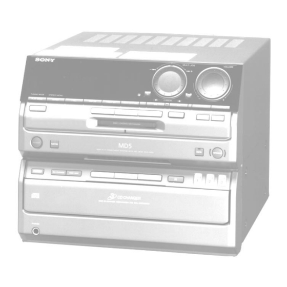
HCD-MD5 is the amplifier, CD, MD
and tuner section in DHC-MD5.
US and foreign patents licensed from Dolby
Laboratories Licensing Corporation.
Amplifier section
DIN power output
40 W + 40 W
(6 ohms, at 1 kHz, DIN)
Continuous RMS power output
50 + 50 watts
(6 ohms at 1 kHz, 10% THD)
Peak music power output
700 watts
Music power output
160 watts
Inputs
VIDEO/GAME IN
(phono jacks)
(switchable)
VIDEO IN:
voltage 250 mV,
impedance 47 kilohms
GAME IN:
voltage 450 mV,
impedance 47 kilohms
TAPE IN (phono jacks):
voltage 250mV,
impedance 47 kilohms
Outputs
TAPE OUT (phono jacks):
voltage 250 mV
impedance 1 kilohms
PHONES (stereo phone jack):
accepts headphones of
8 ohms or more.
SPEAKER:
accepts impedance of 6 to
16 ohms.
MICROFILM
HCD-MD5
CD
Section
MD
Section
SPECIFICATIONS
CD player section
System
Compact disc and digital
audio system
Laser
Semiconductor laser
(λ=780 nm)
Emission duration:
continuous
Laser output
Max. 44.6 µW*
*This output is the value
measured at a distance of
200 mm from the objective
lens surface on the Optical
Pick-up Block with 7 mm
aperture.
Frequency response
2 Hz – 20 kHz (±0.5 dB)
CD OPTICAL DIGITAL OUT
(Square optical connector jack, rear panel)
MINI Hi-Fi COMPONENT SYSTEM
Tourist Model
Model Name Using Similar Mechanism
CD Mechanism Type
Base Unit Name
Optical Pick-up Name
Model Name Using Similar Mechanism
MD Mechanism Type
Base Unit Name
Optical Pick-up Name
MD deck section
System
Laser
Laser output
Recording time
Sampling frequency
Frequency response
AEP Model
UK Model
E Model
HCD-W55
CDM38A-5BD19
BU-5BD19
KSS-213B/K-N
NEW
MDM-2FR
MBU-2F
KMS-210A/J-N
MiniDisc digital audio
system
Semiconductor laser
(λ=780 nm)
Emission duration:
continuous
Max. 44.6 µW*
*This output is the value
measured at a distance of
200 mm from the objective
lens surface on the Optical
Pick-up Block with a
7 mm aperture.
74 minutes max. (using
MDW-74)
44.1 kHz
5 Hz to 20 kHz
– Continued on next page –
Advertisement
Table of Contents

Related Manuals for Sony HCD-MD5


Summary of Contents for Sony HCD-MD5
- Page 1 HCD-MD5 SERVICE MANUAL AEP Model UK Model E Model Tourist Model HCD-MD5 is the amplifier, CD, MD and tuner section in DHC-MD5. Model Name Using Similar Mechanism HCD-W55 US and foreign patents licensed from Dolby Laboratories Licensing Corporation. CD Mechanism Type...
-
Page 2: Table Of Contents
(20 lb 12 oz) Supplied accessories: AM loop aerial (1) ELECTRICAL PARTS LIST ........132 Remote RM-S5MD (1) Sony SUM-3 (NS) batteries (2) FM lead aerial (1) Speaker cords (2) Design and specifications are subject to change without notice. – 2 –... - Page 3 LINE WITH MARK ! ON THE SCHEMATIC DIAGRAMS AND IN THE PARTS LIST ARE CRITICAL TO SAFE OPERATION. REPLACE THESE COMPONENTS WITH SONY PARTS WHOSE PART NUMBERS APPEAR AS SHOWN IN THIS MANUAL OR IN SUPPLEMENTS PUB- LISHED BY SONY.
- Page 4 COLD START METHOD While pressing the POWER key, insert the AC plug cord into the AC outlet. Cold start will be set. Note : As cold start will erase all the preset contents etc., do not set it in normal operations. FORCED RESET SWITCH The switch on the power board (S101) is the forced reset switch for IC201.
- Page 5 SECTION 2 This section is extracted from instruction manual. GENERAL – 5 –...
- Page 6 – 6 –...
-
Page 7: Disassembly
SECTION 3 DISASSEMBLY Note: Follow the disassembly procedure in the numerical order given. CASE, FRONT PANEL ASS’Y 1 four screws 2 case (CASE 3 TP2) 1 four screws (CASE 3 TP2) 4 connector (CN906) 3 flat wire (22 core) 1 four screws (CN103) (CASE 3 TP2) 3 flat wire (19 core) - Page 8 BRACKET (MAIN) SECTION 6 bracket (MAIN) section 5 three screws (BV3 × 8) 1 four screws (BV3 × 8) 3 cover (FFC) 2 supplied OPT cap 4 flat wire (21 core) (CN807) 1 three screws (BV3 × 8) 5 three screws (BV3 ×...
- Page 9 CD MECHANISM 2 CD mechanism 1 two boss MD MECHANISM SECTION 2 three screws (BV3 × 8) 2 screw (BV3 × 8) 3 cover (MDM) (AEP, UK, German) 4 MD mechanism section 1 connector (CN101) – 9 –...
- Page 10 DISC TRAY flat wire 3 flat wire (8 core) claw A claw B Note: When mounting the disc tray, route a flat 4 two claws cable through claw A and B as shown in the figure. 2 Pull the disc tray. 5 Remove the disc tray.
- Page 11 INSTALLATION DISC TRAY Note: When mounting the disc tray, the collars A and B must be engaged in the grooves respectively. callar A callar B ditch SLIDER (M) ASS’Y claw B claw A 1 Remove a torsion coil spling from the claw A . 2 Disengaging the claw B , raise the lever (SLM) upward to remove.
- Page 12 INSTALLATION BU CAM ASS’Y BASE UNIT, ROTALY ENCODER When mounting the base unit, insert the portion A into a groove in the BU cam. portion A When mounting the BU cam assembly, it must be engaged with the rotaly encorder switch as shown. BASE UNIT, LOADING MOTOR ASS’Y 3 belt 4 two screws...
- Page 13 INSTALLATION SLIDER (M) ASS’Y 2 Slide the slider (M) assembly toward direction B unit it can be locked with the lever (SLM). 1 Turn fully the lever (SLM) toward direction A . – 13 –...
-
Page 14: Test Mode
SECTION 4 TEST MODE 4-2-3. Operating the Check Mode Note: * When the following keys are pressed in the check mode state (Re- Be sure to connect all wires (including FFC) in the MD fer to Table 4-1.), the switching state of the DBFB, VOLUME, section before applying power or ICs may be damaged. - Page 15 4-4. FLUORESCENT INDICATOR TUBE AND 3. If errors occur during or after aging, the error messages in the following table will be displayed. CHECK MODE FOR KEYS 4-4-1. Setting the Check Mode Table 4-2. • Turn OFF the power of the unit, and set the check mode by press- Error Message Contents ing the following keys together.
- Page 16 4-6. CHECK MODE FOR CLOCK FUNCTION When the MUTLI JOG dial and VOLUME control dial are rotated, the JOG count display will count up or down accordingly. 4-6-1. Setting and Operating the Check Mode (E.g.) 1. Turn OFF the power of the unit. 2.
- Page 17 4-7. TEST MODE FOR MD SECTION 4-7-5. Operating the Continuous Playback Mode 1. Entering the continuous playback mode 4-7-1. Setting the Test Mode • Turn OFF the power of the unit, and set the test mode by pressing 1) Set the disk in the unit (either MO or CD). 2) Turning the MULTI JOG dial and display “CPLAY MODE”.
- Page 18 2. The EDIT/NO key can be used to stop recording anytime. 4-7-8. Test Mode Displays • Each time the DISPLAY key pressed, the display changes in the 3. During the test mode, the erasing-protection tab will not be detected. Therefore be carefull not to set the continuous re- following order.
- Page 19 4-7-9. Meanings of Other Displays 4-7-10. Precautions for Use of Test Mode 1. As loading related operations will be performed regardless of Table 4-6. the test mode operations being performed, be sure to check that the disc is stopped before setting and removing it. Even if the §(MD) key is pressed while the disc is rotating Display Contents...
-
Page 20: Electrical Adjustments
SECTION 5 ELECTRICAL ADJUSTMENTS 5-3. PRECAUTIONS FOR ADJUSTMENTS Note: 1) When replacing the following parts, perform the adjustments Be sure to connect all wires (including FFC) in the MD and checks with ® in the order shown in the following table. section before applying power or ICs may be damaged. - Page 21 5-5. TEMPERATURE COMPENSATION OFFSET 5-6. LASER POWER ADJUSTMENT ADJUSTMENT Connection: Save the temperature data at that time in the non-volatile memory laser as 25°C reference data. power meter Note: 1. Usually, do not perform this adjustment. 2. Perform this adjustment in an ambient temperature of 22°C to Optical pick-up 28°C.
- Page 22 5-7. TRAVERSE (E-F BALANCE) ADJUSTMENT 11. Turning the MULTI JOG dial until the waveforms of the oscil- loscope moves closer to the specified value. Note 1) Data will be erased during MO reading if a recorded In this adjustment, waveform varies at intervals of approx. 3%. disc is used in this adjustment.
- Page 23 5-8. FOCUS BIAS ADJUSTMENT 5-9. ERROR RATE CHECK Adjusting Method: 5-9-1. CD Error Rate Check 1. Load a continuously recorded disc (Refer to “5-4. Creating MO Checking Method: Continuously Recorded Disc”.) 1. Load a test disc TDYS-1. 2. Turning the MULTI JOG dial and display “CPLAY MODE”. 2.
- Page 24 5-11. ADJUSTING POINTS AND CONNECTING POINTS [BD (MD) BOARD] (Side A) D101 IC191 [BD (MD) BOARD] (Side B) (IOP) (I+5V) IC101 RV101 (VC) IC171 RV102 (TEO) IC121 – 24 –...
-
Page 25: Tuner Section
SW OSC Voltage Adjustment (EA, MY, SP, HK model) TUNER SECTION 0 dB=1µV Setting : Precaution in Repairing Band : SW Note : As a front-end (FE1) is difficult to repair if faulty, replace it Procedure : with new one. 1. -
Page 26: Cd Section
Adjustment Location CD SECTION Note : [TCB BOARD] – Component side – 1. Use YEDS-18 disc (3-702-101-01) unless otherwise indicated. 2. Use the oscilloscope with more than 10 MΩ impedance. CV1: SW Tracking Adjustmnet 3. Clean an object lens by an applicator with neutral detergent when T1: SW Tracking Adjustment the signal level is low than specified value with the following checks. - Page 27 Traverse waveform 5. Check the oscilloscope waveform (S-curve) is symmetrical be- tween A and B. And confirm peak to peak level within 2.4 ± 0.7 Vp-p. S-curve waveform symmetry level: 300 ± 100 mVp-p within 2.4 ± 0.7 Vp-p A–B specified level : •...
- Page 28 SECTION 6 DIAGRAMS • Circuit Boards Location TCB board THERMO board MAIN board TRANSFORMER board PANEL A board HEADPHONE board POWER board AMPLIFIER board PANEL B board SENSOR board MOTOR (TURN) board CONNECTOR board BD (MD) board DETECTION SW board MOTOR board BD (CD) board RELAY board...
-
Page 55: Ic Pin Function Description
6-22. IC PIN FUNCTION DESCRIPTION BD (MD) Board IC101 CXA1981AR (RF Amplifier) Pin No. Pin Name Function Middle point voltage (+2.5V) generation Signal input from the optical block detector. F operation amplifier input F operation amplifier output Front monitor. Connected to the photo diode. APCREF Input for laser power setting TEMPI... - Page 56 BD (MD) Board IC121 CXD2535BR (Digital Signal Processing, Digital Servo Signal Processing, EFM/ACIRC Encorder/Decorder) Pin No. Pin Name Function FS256 11.2896 MHz clock output (MCLK system). Not Used (Open). FOK signal output to the MD system control (IC201). “H” is output when focus is on. DFCT Defect signal ON/OFF select signal output to the CXD2538CR (IC271).
- Page 57 Pin No. Pin Name Function WFCK clock (7.35 kHz) signal output (Playback: EFM decoder PLL, Recording: EFM encoder PLL) WFCK (Open) GTOP “H”: Playback EFM frame sync protect window opens. Not used (Open). “H”: Playback EFM frame sync is synchronized with interpolation protect timing. Not used (Open). EFM decoder PLL clock output (98Fs=4.3218 MHz) XPLCK Falling edge are synchronized with EFM signal edge (Open)
- Page 58 Pin No. Pin Name Function TS25 Test pin (Connected to ground). LDDR Laser APC signal output TRDR Tracking servo drive signal output (–) TFDR Tracking servo drive signal output (+) FFDR Focus servo drive signal output (+) DVDD — Power supply (+5V) (Digital system) FRDR Focus servo drive signal output (–) 176.4 kHz clock signal output (MCLK system)
- Page 59 Digital Board IC201 M37610MD-068FP (System Control, Mechanism Controller (MD)) Pin No. Pin Name Function Emphasis ON/OFF select. “H”: ON. It is inverted by the emphasis control Q201 of IC303 and the C, SET 1 inverted signal is input to the IC303. C, SET 0 Not used (Connected to ground).
- Page 60 Pin No. Pin Name Function ATP address sync or subcode Q sync (SCOR) from the CXA2535BR (IC121). ATSY “L” is input every 13.3 msec. Almost all “H”. Input of U-bit CD format subcode Q sync (SCOR) from the CXA2535BR (IC121). DQSY “L”...
- Page 61 Pin No. Pin Name Function AMUTE Line out muting output LDOUT Loading motor (M191) control output *1 LDIN REC SW Detect input from the chucking switch (S193). When chucked: “L”. PLAY SW Loading In switch (S192) detect input “L” at a position where the magnetic head lowers. Others: “H”. OUT SW Loading Out switch (S192) detect input “L”...
- Page 62 Digital Board IC271 CXA2536CR (Shock Proof Memory Controller, ATRAC Encoder/Decoder) Pin No. Pin Name Function — Power supply (+5V) SWDT Writing data signal input from the MD system control (IC201). Serial clock signal input from the MD system control (IC201). XLAT Serial latch signal input from the MD system control (IC201).
- Page 63 Pin No. Pin Name Function ABCK Bit clock signal output to the A/D, D/A converter (IC303). ALRCK L/R clock signal output to the A/D, D/A converter (IC303). Address signal output. Not used (Open). Address signal output. Not used (Open). — Ground —...
- Page 64 Pin No. Pin Name Function — Ground MDSY Main data sync detect signal output (Open) LRCK L/R clock signal input from the CXD2535BR (IC121). (44.1 kHz) Bit clock signal input from the CXD2535BR (IC121). (2.8224 MHz) C2PO signal input (Indicates data error status) from the CXD2535BR (IC121). C2PO Playback: C2PO (“H”), Digital recording: D.
- Page 65 Panel B Board IC501 µPD78058GC-411-3B9 (System Control, Display Control) Pin No. Pin Name Function — — Not used (Open). — — AD converter ground JOGGUIDE.TOP. JOG LED output JOGGUIDE.ENT. ENTER LED output AVREF1 — DA converter reference voltage input Communication with the MD mechanism controller. Reception data input. Communication with the MD mechanism controller.
- Page 66 Pin No. Pin Name Function MD FAN Air-cooling fan control output ST.MUTE ST MUTE output ST CE CE output to LC72130 COM CLK CLOCK output to the LC72130. ST DI Data input from the LC72130. COM DO Data output to the LC72130. GEQ-LAT Latch output to the M62427.
- Page 67 Relay Board IC851 µPD78055GC-055-3B9 (CD Mechanism Controller) Pin No. Pin Name Function BDRST BD reset output RESET A MUTE Muting ON/OFF output. Not used (Open). Mute MUTE DOWN FOCUSSW Focus gain select output. Normal Down NORMAL AVSS — Ground potential of the A/D converter (Connected to VSS.) DRVRST M66004 reset output.
- Page 68 Pin No. Pin Name Function ENCORDE2 Disc tray address detect encoder input 2 AFADJ Not used (Fixed at “H”). TBL-SENSE Table address detect sensor input Present DSC-SENSE Disc present/absent sensor input. Absent OUTSW Disc tray open completion input. Open completion PWMSW Not used (Connected to ground).
-
Page 69: Exploded Views
SECTION 7 EXPLODED VIEWS NOTE: • -XX and -X mean standardized parts, so they • Items marked “*” are not stocked since they The components identified by mark ! or dotted line with mark ! are may have some difference from the original are seldom required for routine service. - Page 70 * 17 A-4392-035-A PANEL B BOARD, COMPLETE (SP, MY) 4-969-236-01 SPRING (LID), TORSION * 18 A-4390-886-A PANEL A BOARD, COMPLETE (EA, HK) 4-962-708-01 EMBLEM (4-A), SONY * 18 A-4390-894-A PANEL A BOARD, COMPLETE (AEP, G) 4-984-196-01 KNOB (VOL) * 18...
- Page 71 (2) CHASSIS SECTION supplied not supplied not supplied EXCEPT UK, HK UK, HK supplied CNP801 JE, SP, MY AEP, G, EA, HK, supplied SP, MY M901 CNP801 T901 supplied CNP801 supplied CDM38A-5BD19 MDM-2FR supplied supplied supplied – 125 –...
- Page 72 Ref. No. Part No. Description Remark Ref. No. Part No. Description Remark * 51 A-4390-907-A DIGITAL BOARD, COMPLETE * 61 3-703-571-11 BUSHING (S) (4516), CORD (JE) 1-777-471-11 WIRE (FLAT TYPE) (18 CORE) * 62 1-662-206-11 TRANSFORMER BOARD 1-777-470-11 WIRE (FLAT TYPE) (30 CORE) * 63 4-984-208-11 PANEL, BACK (AEP) 1-777-475-11 WIRE (FLAT TYPE) (23 CORE)
- Page 73 (3) MD MECHANISM SECTION (MDM-2FR) supplied supplied M191 NBU-2F supplied supplied Ref. No. Part No. Description Remark Ref. No. Part No. Description Remark 4-967-673-01 SPRING, COMPRESSION 4-983-110-01 CUSHION (LVO) 4-967-671-01 INSULATOR (MD) 4-977-777-01 BASE (BD) 4-970-710-01 SPRING, COMPRESSION 4-967-669-01 LEVER (UDR) 4-979-400-01 LEVER (DOOR) 4-967-670-01 SPRING (UDR), TORSION 4-983-100-01 COLLAR (DAMPER)
- Page 74 (4) MD BASE UNIT SECTION (MBU-2F) S102 HR901 not supplied supplied M102 M101 Ref. No. Part No. Description Remark Ref. No. Part No. Description Remark * 151 A-4673-656-A BD (MD) BOARD, COMPLETE 4-967-675-01 GEAR (SL-A) 4-967-679-01 SPRING (OP), LEAF HR901 1-500-304-21 HEAD, OVER LIGHT ! 153 8-583-009-11 OPTICAL PICK-UP (MD) KMS-210A/J-N...
- Page 75 (5) CD MECHANISM SECTION-1 (CDM38A-5BD19) M1701 CD mechanism section-2 Ref. No. Part No. Description Remark Ref. No. Part No. Description Remark * 201 1-662-213-11 SENSOR BOARD 4-977-943-01 BELT (TURN) (1.2) 4-981-187-01 COLLAR (WORM) * 208 1-662-212-11 MOTOR (TURN) BOARD X-4946-295-2 SHAFT ASSY, WORM 4-977-941-01 BEARING (WORM) 4-977-956-01 WHEEL, WORM 4-977-944-01 TRAY (SLIDE)
- Page 76 (6) CD MECHANISM SECTION-2 (CDM38A-5BD19) M1801 BU-5BD19 S851 Ref. No. Part No. Description Remark Ref. No. Part No. Description Remark X-4946-296-1 HOLDER (BU) ASSY 4-977-942-01 BELT (SL) (1.4) 4-982-447-01 SPRING (BU), COMPRESSION X-4946-491-1 CAM ASSY, BU 4-985-672-01 SCREW (+PTPWH M2.6), FLOATING * 262 1-452-879-11 MAGNET * 254...
- Page 77 (7) CD BASE UNIT SECTION (BU-5BD19) M101 M102 Ref. No. Part No. Description Remark Ref. No. Part No. Description Remark 4-951-620-01 SCREW (2.6X8), +BVTP 1-769-069-11 WIRE (FLAT TYPE) (16 CORE) * 302 A-4673-402-A BD (CD) BOARD, COMPLETE 4-917-567-01 GEAR (M) 4-951-940-01 INSULATOR (BU) 4-917-564-01 GEAR (P), FLATNESS 4-917-565-01 SHAFT, SLED...
-
Page 78: Electrical Parts List
SECTION 8 AMPLIFIER ELECTRICAL PARTS LIST NOTE: • Due to standardization, replacements in the • SEMICONDUCTORS The components identified by mark In each case, u: µ, for example: parts list may be different from the parts speci- ! or dotted line with mark ! are criti- uA. - Page 79 AMPLIFIER BD (CD) Ref. No. Part No. Description Remark Ref. No. Part No. Description Remark < TRANSISTOR > R958 1-249-425-11 CARBON 4.7K 1/4W R959 1-249-425-11 CARBON 4.7K 1/4W Q901 8-729-661-94 TRANSISTOR RT1N141SK-TP Q902 8-729-140-84 TRANSISTOR 2SC1841-PAFAEA R960 1-249-397-11 CARBON 1/4W Q952 8-729-140-84 TRANSISTOR 2SC1841-PAFAEA R961...
- Page 80 BD (CD) Ref. No. Part No. Description Remark Ref. No. Part No. Description Remark C108 1-164-232-11 CERAMIC CHIP 0.01uF IC102 8-759-291-06 IC BA6397FP C109 1-164-232-11 CERAMIC CHIP 0.01uF IC103 8-752-372-94 IC CXD2507AQ C110 1-163-989-11 CERAMIC CHIP 0.033uF IC104 8-759-185-29 IC PCM1710U-B C111 1-163-038-00 CERAMIC CHIP 0.1uF...
- Page 81 BD (CD) BD (MD) Ref. No. Part No. Description Remark Ref. No. Part No. Description Remark R143 1-216-121-91 METAL GLAZE 1/10W C115 1-107-682-11 CERAMIC CHIP C116 1-163-019-00 CERAMIC CHIP 0.0068uF 10% R144 1-216-073-00 METAL CHIP 1/10W R145 1-216-097-00 METAL GLAZE 100K 1/10W C117...
- Page 82 BD (MD) Ref. No. Part No. Description Remark Ref. No. Part No. Description Remark C192 1-163-038-00 CERAMIC CHIP 0.1uF Q163 8-729-905-12 TRANSISTOR DTA144EU C193 1-164-346-11 CERAMIC CHIP Q164 8-729-924-19 TRANSISTOR DTA123JU C194 1-126-206-11 ELECT CHIP 100uF 6.3V Q181 8-729-018-75 TRANSISTOR 2SJ278MY <...
- Page 83 BD (MD) CONNECTOR DETECTION SW DIGITAL Ref. No. Part No. Description Remark Ref. No. Part No. Description Remark R154 1-220-262-11 METAL GLAZE 1/4W R155 1-220-262-11 METAL GLAZE 1/4W 1-653-411-11 DETECTION SW BOARD R158 1-216-121-00 METAL GLAZE 1/10W ******************* R161 1-216-057-00 METAL CHIP 2.2K 1/10W <...
- Page 84 DIGITAL Ref. No. Part No. Description Remark Ref. No. Part No. Description Remark C312 1-164-346-11 CERAMIC CHIP < FERRITE BEAD > C313 1-126-204-11 ELECT CHIP 47uF C314 1-163-038-00 CERAMIC CHIP 0.1uF FB272 1-550-907-21 BEAD, FERRITE (CHIP) FB274 1-216-295-00 CONDUCTOR, CHIP (2012) C315 1-163-017-00 CERAMIC CHIP...
- Page 85 DIGITAL Ref. No. Part No. Description Remark Ref. No. Part No. Description Remark R243 1-216-097-00 METAL GLAZE 100K 1/10W R321 1-216-295-00 CONDUCTOR, CHIP (2012) R244 1-216-073-00 METAL CHIP 1/10W R322 1-216-295-00 CONDUCTOR, CHIP (2012) R361 1-216-687-11 METAL CHIP 0.5% 1/10W R245 1-216-049-00 METAL GLAZE 1/10W...
- Page 86 HEADPHONE MAIN Ref. No. Part No. Description Remark Ref. No. Part No. Description Remark C153 1-136-169-00 FILM 0.22uF R646 1-550-907-21 BEAD, FERRITE (CHIP) C154 1-136-169-00 FILM 0.22uF < VIBRATOR > C155 1-136-163-00 FILM 0.068uF C156 1-136-163-00 FILM 0.068uF X201 1-760-493-11 VIBRATOR, CERAMIC (CHIP TYPE) (8MHz) C157 1-136-156-00 FILM 0.018uF...
- Page 87 MAIN Ref. No. Part No. Description Remark Ref. No. Part No. Description Remark C1031 1-124-464-11 ELECT 0.22uF < IC > C7001 1-101-884-00 CERAMIC 56PF (AEP, G, UK) IC105 8-759-331-39 IC M62427FP C7002 1-101-884-00 CERAMIC 56PF IC701 8-759-000-48 IC MC14052BCP (AEP, G, UK) IC702 8-759-000-48 IC MC14052BCP IC703...
- Page 88 MAIN Ref. No. Part No. Description Remark Ref. No. Part No. Description Remark R154 1-247-807-31 CARBON 1/4W R751 1-249-435-11 CARBON 1/4W (AEP, G, UK) R752 1-249-427-11 CARBON 6.8K 1/4W R155 1-247-807-31 CARBON 1/4W R755 1-247-807-31 CARBON 1/4W (AEP, G, UK) R757 1-249-441-11 CARBON 100K...
- Page 89 MOTOR (SLIDE) MOTOR (TURN) MOTOR PANEL A Ref. No. Part No. Description Remark Ref. No. Part No. Description Remark < VIBRATOR > R1706 1-249-411-11 CARBON 1/4W X7001 1-579-900-21 VIBRATOR, CRYSTAL (4.332MHz)(AEP, G, UK) R1707 1-249-401-11 CARBON 1/4W ************************************************************ ************************************************************ 1-662-214-11 MOTOR (SLIDE) BOARD 1-653-412-11 MOTOR BOARD ******************* *************...
- Page 90 PANEL A PANEL B Ref. No. Part No. Description Remark Ref. No. Part No. Description Remark C538 1-162-290-31 CERAMIC 470PF R575 1-249-409-11 CARBON 1/4W C539 1-162-290-31 CERAMIC 470PF R576 1-249-409-11 CARBON 1/4W C540 1-162-290-31 CERAMIC 470PF C541 1-162-290-31 CERAMIC 470PF <...
- Page 91 PANEL B Ref. No. Part No. Description Remark Ref. No. Part No. Description Remark D516 8-719-987-63 DIODE 1N4148M R527 1-249-429-11 CARBON 1/4W (G, JE) D518 8-719-987-63 DIODE 1N4148M R528 1-249-429-11 CARBON 1/4W D519 8-719-987-63 DIODE 1N4148M (MY, SP, EA, HK, JE) D520 8-719-010-48 DIODE UZ-6.8BS R530...
- Page 92 PANEL B POWER Ref. No. Part No. Description Remark Ref. No. Part No. Description Remark (AEP, G, UK) S530 1-571-760-11 SWITCH, KEY BOARD (DISC 1) R609 1-247-807-31 CARBON 1/4W S531 1-571-760-11 SWITCH, KEY BOARD (DISC 2) R610 1-247-807-31 CARBON 1/4W S532 1-571-760-11 SWITCH, KEY BOARD (DISC 3) R611...
- Page 93 POWER Ref. No. Part No. Description Remark Ref. No. Part No. Description Remark C819 1-126-967-11 ELECT 47uF D116 8-719-987-63 DIODE 1N4148M C820 1-126-974-11 ELECT 3300uF D117 8-719-987-63 DIODE 1N4148M C821 1-126-974-11 ELECT 3300uF C822 1-162-306-11 CERAMIC 0.01uF D801 8-719-014-74 DIODE UZP-6.2B C823 1-162-306-11 CERAMIC 0.01uF...
- Page 94 POWER Ref. No. Part No. Description Remark Ref. No. Part No. Description Remark < IC > R805 1-249-415-11 CARBON 1/4W IC102 8-759-917-18 IC SN74HCU04AN R806 1-247-850-11 CARBON 6.2K 1/4W IC103 8-759-327-15 IC M62005L R807 1-249-416-11 CARBON 1/4W IC801 8-759-231-58 IC TA7812S R808 1-247-843-11 CARBON 3.3K...
- Page 95 RELAY SENSOR Ref. No. Part No. Description Remark Ref. No. Part No. Description Remark R862 1-247-807-31 CARBON 1/4W S101 1-572-184-11 SWITCH, KEYBOARD (RESET) R867 1-247-843-11 CARBON 3.3K 1/4W R868 1-247-843-11 CARBON 3.3K 1/4W ************************************************************ R869 1-247-843-11 CARBON 3.3K 1/4W A-4390-896-A RELAY BOARD, COMPLETE (AEP, G) R870 1-247-843-11 CARBON 3.3K...
- Page 96 Ref. No. Part No. Description Remark Ref. No. Part No. Description Remark 1-126-964-11 ELECT 10uF 1-163-038-00 CERAMIC CHIP 0.1uF 1-126-964-11 ELECT 10uF (EA, MY, SP, HK, JE) 1-104-396-11 ELECT 10uF 1-216-295-00 METAL CHIP 1/10W 1-104-396-11 ELECT 10uF 1-163-038-00 CERAMIC CHIP 0.1uF 1-104-396-11 ELECT 10uF...
- Page 97 Ref. No. Part No. Description Remark Ref. No. Part No. Description Remark 1-233-532-11 FRONTEND (EA, MY, SP, HK) 1-410-521-11 MICROINDUCTOR 100uH 1-233-542-11 FRONTEND (4GAND) (AEP, G, UK) (EA, MY, SP, HK,JE) 1-693-251-11 FRONTEND (JE) 1-414-142-11 MICROINDUCTOR 1uH (AEP, G, UK) 1-233-514-11 ENCAPSULATED COMPONENT (AEP, UK) 1-410-521-11 MICROINDUCTOR 100uH 1-239-260-11 ENCAPSULATED COMPONENT (G)
- Page 98 THERMO TRANSFORMER Ref. No. Part No. Description Remark Ref. No. Part No. Description Remark (AEP, UK) (AEP, UK, EA, MY, SP, HK, JE) 1-216-065-00 METAL CHIP 4.7K 1/10W < VARIABLE RESISTOR > (EA, MY, SP, HK, JE) 1-216-073-00 METAL CHIP 1/10W RV41 1-238-601-11 RES,ADJ,CARBON 22K...
- Page 99 TRANSFORMER Ref. No. Part No. Description Remark Ref. No. Part No. Description Remark ! F953 1-532-465-51 FUSE, TIME LAG (3.15A/250V) ! T901 1-429-787-11 TRANSFORMER, POWER (EA, HK, SP, MY, JE) ! F954 1-532-465-51 FUSE, TIME LAG (3.15A/250V) ************************************************************ ! F955 1-532-464-51 FUSE (2.5A/250V) ! F956 1-532-464-51 FUSE (2.5A/250V)
- Page 100 HCD-MD5 English 96H0573-1 Printed in Japan Sony Corporation © 1996. 8 9-960-713-11 Home A&V Products Company Published by Quality Engineering Dept. (Shibaura) – 154 –...
- Page 101 HCD-MD5 AEP Model UK Model SERVICE MANUAL E Model Tourist Model SUPPLEMENT-1 File this supplement with the service manual. Subject: Addition of IC123 (SFD-00002) : Addition portion Page 57 Location: G-3, 4 Page 65, 66 Location: F-19-I-25 Page FORMER Ref. No.