
Related Manuals for Panasonic SA-PM53E


Summary of Contents for Panasonic SA-PM53E
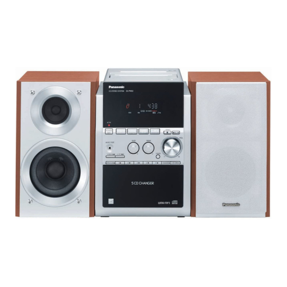
- Page 1 ORDER NO. MD0602043C2 CD Stereo System SA-PM53E / SA-PM53EB / SA-PM53EG Colour (S)... Silver Type SPECIFICATIONS Specification...
- Page 2 Amplifier Section RMS OUTPUT POWER both channel driven 10% Total harmonic distortion 1 kHz 50 W per channel (6 Total Bi-Amp power 90 W per channel Input Impedance 250 mV 12k Output Impedance Headphone to 32 Phone jack Terminal Stereo, 3.5 mm AUX jack (Music port) Terminal Stereo, 3.5 mm...
-
Page 3: Safety Precautions
2. Total harmonic distortion is measured by the digital spectrum analyzer. 3. The labels “HIGH” and “LOW” on the rear or the speakers refer to High frequency and Low frequency. Music center: SA-PM53E-S System : SC-PM53E-S Speaker: SB-PM53EG-MJ Music center: SA-PM53EB-S... - Page 4 1. When servicing, observe the original lead dress. If a short circuit is found, replace all parts which have been overheated or damaged by the short circuit. 2. After servicing, ensure that all the protective devices such as insulation barriers, insulation papers shields are properly installed. 3.
- Page 5 measurements. 6. The potential at any point should not exceed 0.75 volts RMS. A leakage current tester (Simpson Model 229 or equivalent) may be used to make the hot checks, leakage current must not exceed 1/2 milliamp. should the measurement is outside of the limits specified, there is a possibility of a shock hazard, and the equipment should be repaired and re- checked before it is returned to the customer.
-
Page 6: Before Repair And Adjustment
1.3. Before Repair and Adjustment Disconnect AC power, discharge Power Supply Capacitors C512, C513, C514, C606, C608, C610, C624 through a 10 , 1W resistor to ground. DO NOT SHORT-CIRCUIT DIRECTLY (with a screwdriver blade, for instance), as this may destroy solid state devices. -
Page 7: Precaution Of Laser Diode
3. Use only a grounded-tip soldering iron to solder or unsolder ES devices. 4. Use only an anti-static solder removal device. Some solder removal devices not classified as “anti-static (ESD protected)” can generate electrical charge to damage ES devices. 5. Do not use freon-propelled chemicals. These can generate electrical charges sufficient to damage ES devices. - Page 8 3. Do not look at the focus lens using optical instruments. 4. Recommend not to look at pick up lens for a long time. ACHTUNG : Dieses Produkt enthält eine Laserdiode. Im eingeschalteten Zustand wird unsichtbare Laserstrahlung von der Lasereinheit abgestrahlt. / Wellenlänge : 780nm / Maximale Strahlungsleistung der Lasereinheit : W/VDE / Die Strahlung an der Lasereinheit ist ungefährlich, wenn folgende Punkte beachtet werden:...
-
Page 9: Handling Precautions For Traverse Deck
4. Handling Precautions For Traverse Deck The laser diode in the traverse deck (optical pickup) may break down due to potential difference caused by static electricity of clothes or human body. So, be careful of electrostatic breakdown during repair of the traverse deck (optical pickup). - Page 10 2. Work table grounding. (Fig 4.2) / Put a conductive material (sheet) or steel sheet on the area where the traverse deck (optical pickup) is place, and ground the sheet. Caution: The static electricity of your clothes will not be grounded through the wrist strap.
-
Page 11: Handling The Lead-Free Solder
5. Handling the Lead-free Solder 5.1. About lead free solder (PbF) Distinction of PbF P.C.B.: P.C.B.s (manufactured) using lead free solder will have a PbF stamp on the P.C.B. Caution: - Pb free solder has a higher melting point than standard solder; Typically the melting point is 50 - 70°F (30 - 40°C) higher. - Page 12 AC Power Cord / (For E/EG) AM Loop Antenna FM Antenna FM Antenna (For EB) 7. Operating Instructions Procedures 7.1. Main Unit & Remote Control Operation 7.2. Disc Information 8. Self-Diagnosis & Special Mode Setting...
- Page 13 This unit is equipped with features of self-diagnostic & special mode setting for checking the functions & reliability. Special Note : Checking of the reliability (ageing) & changer operation must be carry out to ensure good working condition in unit. 8.1.
- Page 14 Item FL Display Key Operation Mode Name Description Front Key Doctor Mode To enter into In any mode: Doctor Mode for checking of 1. Press [ ] button various items and on main unit follow by [4] and [7] on remote 1.
- Page 15 Item FL Display Key Operation Mode Name Description Front Key Tape To Inspect the In doctor mode: 1. Press [6] button on remote control. Recording Tape recording and Playing and playing is To exit, press [ENTER] button on process for unit. remote control or (For more information, refer...
- Page 16 Item FL Display Key Operation Mode Name Description Front Key Changer To check the CD In doctor mode: 1. Press [DISC] button on remote control. Operation Changer Operation. To exit, press [ENTER] button on (For more remote control or information, refer to section 8.1.7) 1.
- Page 17 Operation Procedures Micon operation & processing C-mecha Abnormal Detection shall Check that all DECK mechanism leaf SW is in OFF state. be executed for DECK 1 only. FF shall be executed for 2 sec, after which STOP. / Check the following. / { F.REC INH SW } is OFF / { R.REC ] key is INH SW } is ON / { HALF SW } is ON / Reel pulse toggles pressed, after loading in a...
- Page 20 8.1.3. EEPROM Checksum (ROM correction) Purpose : To check for micro-processor firmware version & EEPROM check (ROM correction). Below is the procedures for this mode. Step 1: Enter into Doctor mode (For more information refer to section 8.1 on key operation to enter into this mode).
- Page 21 3. When EEPROM IC is detected and has ROM correction but NG: Note: Micro-processor firmware version refers to version No. (Eg.MS079_12) for micro-processor IC. It is subject to change which would update accordingly. - Rom correction checksum refers to the hex code that is display upon key buttons pressed if an EEPROM is loaded in the unit.
- Page 22 tab for FWD side is not suitable for recording. - When in this mode, if button is pressed the process will stops automatically. 8.1.5. Tape Recording and Playing Assuming the recording to TAPE has been done in test 3, only playing TAPE is made. Purpose : To check the Tape function.
- Page 24 8.1.6. TPS Inspection Purpose : To check the TPS. Below is the procedures for this mode. Step 1: Enter into Doctor mode (For more information refer to section 8.1 on key operation to enter into this mode). Step 2 : Press [ ] button on remote control.
- Page 25 8.1.7. RDS Checking Purpose : To check the RDS Function. Below is the procedures for this mode. Step 1: Enter into Doctor mode (For more information refer to section 8.1 on key operation to enter into this mode). Step 2 : Press [DISPLAY] button on remote control. Enter into RDS checking. (During this mode) - BASS and TREBLE set to 0dB and preset EQ OFF.
- Page 26 8.1.8. CR 16 Self Diagnostic - In order to improve the analysis of faulty condition in CR16 mechanism, CR16 related error codes have been further divided. Mode Present After modify Description Initialize F17P Play F22L Load F22T Trouble F22U Unload F27T Trouble F27P...
- Page 27 Mode Present After modify Description NAOU Normal all open up NAOD Normal all open down NACU Normal all close up NACD Normal all close down NACL Normal all close NAOP Normal all open All open / close during PAOU Play all open up play PAOD Play all open down...
-
Page 28: Error Code Table
3. To clear the error code memory In "CR16 Self Diagnostic mode", long press [CD CHECK] key (2s or more). 4. To exit CR16 Self Diagnostic mode Turn off the set. 8.2. Error Code Table Self-Diagnosis Function provides information on any problems occuring for the units and its respective parts by displaying error codes. - Page 29 Error Diagnosis Description of error Automatic FL Display Remarks Code Contents MODE SW For deck mechanism unit (For abnormal deck 1/2). Press [ on main unit for next error. REC INH SW For deck mechanism unit (For abnormal deck 2). Press [ on main unit for next error.
- Page 30 Error Diagnosis Description of error Automatic FL Display Remarks Code Contents Communication CD function DTMS For CD unit (For Traverse). between CD command, after servo LSI and system setting, If Press [ micro-p SENSE = 'L' cannot on main unit for next error. abnormal.
- Page 31 Error Diagnosis Description of error Automatic FL Display Remarks Code Contents SLIDE During vertical For CD unit (For Traverse). OPERATION operation, if failsafe Abnormal. timer is finished and Press [ switch no change or on main unit for next error. switch target condition was not achieve, this error...
-
Page 32: Assembling And Disassembling
Error Diagnosis Description of error Automatic FL Display Remarks Code Contents POWER During normal For Power Supply Related operation, if DCDET Error Detection. output becomes "L", abnormal normal POWER OFF Press [ process shall not be on main unit for next error. executed, PCONT shall be switched to "L"... -
Page 33: Disassembly Flow Chart
Die Lasereinheit nicht zerlegen. Die Lasereinheit darf nur gegen eine vom Hertsteller spezifizierte Einheit ausgetauscht werden. Below is the list of disassembly sections - Disassembly of Side Panel L & R - Disassembly of Top Cabinet - Disassembly of Deck P.C.B. and Tape Eject P.C.B. - Disassembly of Front Panel - Disassembly of Panel P.C.B. - Page 34 9.4. Disassembly of Side Panel L & R - Disassembly of Side Panel (R) Step 1 : Remove 5 screws from the side panel (R). Step 2 : Remove 1 screw from the corner of the side panel (R). Step 3 : Remove the side panel as arrow shown (Be careful of the catches). - Disassembly of Side Panel (L)
-
Page 35: Disassembly Of Top Cabinet
Step 4 : Remove 5 screws from the side panel (L). Step 5 : Remove 1 screw from the corner of the side panel (L). Step 6 : Remove the side panel as arrow shown (Be careful of the catches). 9.5. - Page 36 Step 2 : Place the top cabinet as shown and detach the connector CN1305. 9.6. Disassembly of Deck P.C.B. and Tape Eject P.C.B. - Follow the (Step 1) - (Step 6) of item 9.4. - Follow the (Step 1) - (Step 2) of item 9.5. Step 1 : Remove 1 screw.
-
Page 37: Disassembly Of Front Panel
Step 3 : Remove 4 screws. Step 4 : Push the lever as arrow shown to remove the Deck Mechanism. 9.7. Disassembly of Front Panel - Follow the (Step 1) - (Step 6) of item 9.4. - Follow the (Step 1) - (Step 2) of item 9.5. Step 1 : Detach the connector CN401 and CN501. -
Page 38: Disassembly Of Panel P.c.b
Step 3 : Release 2 catches. Step 4 : Release the catch at the bottom cabinet and remove the front panel as arrow shown. 9.8. Disassembly of Panel P.C.B. - Follow the (Step 1) - (Step 6) of item 9.4. - Follow the (Step 1) - (Step 2) of item 9.5. -
Page 39: Disassembly Of Rear Cabinet
Step 2 : Remove 2 screws and remove the shield plate. Step 3 : Remove 8 screws . Step 4 : Release 1 clutch and remove the Panel P.C.B. 9.9. Disassembly of Rear Cabinet - Follow the (Step 1) - (Step 6) of item 9.4. - Follow the (Step 1) - (Step 2) of item 9.5. -
Page 40: Disassembly Of Main P.c.b
Step 1 : Detach the connector CN300. Step 2 : Remove 7 screws altogether. Step 3 : Remove the rear cabinet as arrows shown (Be careful of the catches). 9.10. Disassembly of Main P.C.B. - Follow the (Step 1) - (Step 6) of item 9.4. - Follow the (Step 1) - (Step 2) of item 9.5. -
Page 41: Disassembly Of Transformer P.c.b
Step 1 : Detach the connector CN401, CN350 and CN351. Step 2 : Detach the connectors CN200 and CN402 and pull out the Main P.C.B. as arrow shown. 9.11. Disassembly of Transformer P.C.B. - Follow the (Step 1) - (Step 6) of item 9.4. - Follow the (Step 1) - (Step 2) of item 9.5. -
Page 42: Disassembly Of Tuner Pack
Step 1 : Detach 2 connectors CN501. Step 2 : Remove 4 screws and pull out the Transformer P.C.B. as arrow shown. 9.12. Disassembly of Tuner Pack - Follow the (Step 1) - (Step 6) of item 9.4. - Follow the (Step 1) - (Step 2) of item 9.5. - Follow the (Step 1) - (Step 3) of item 9.9. -
Page 43: Disassembly Of Power P.c.b
Step 1 : Unsolder Z301 and remove the tuner pack as arrow show. 9.13. Disassembly of Power P.C.B. - Follow the (Step 1) - (Step 6) of item 9.4. - Follow the (Step 1) - (Step 2) of item 9.5. - Follow the (Step 1) - (Step 3) of item 9.9. - Page 44 - Follow the (Step 1) - (Step 4) of item 9.7. Step 1 : Remove 2 screws. Step 2 : Detach the connectors CN350 and CN351. Step 3 : Remove the tape which used to secure the FFC connectors.
-
Page 45: Replacement Of Cd Lid
Step 4 : Release the catches and remove the middle block as arrow shown. Step 5 : Remove 2 screws and remove the CD Mechanism Unit from the bottom chassis as arrow shown. 9.15. Replacement of CD Lid... - Page 46 - Follow the (Step 1) - (Step 6) of item 9.4. - Follow the (Step 1) - (Step 2) of item 9.5. - Follow the (Step 1) - (Step 4) of item 9.7. Step 1 : Remove 2 screws and 2 CD Lid supports. Step 2 :Release the spring hook as arrow shown.
-
Page 47: Replacement Of Cassette Lid
Step 3 : Remove the Inner CD Lid as arrow shown. Step 4 : Remove the CD Lid as arrow shown. 9.16. Replacement of Cassette Lid - Follow the (Step 1) - (Step 6) of item 9.4. - Follow the (Step 1) - (Step 2) of item 9.5. - Follow the (Step 1) - (Step 4) of item 9.6. - Page 48 Step 1 : Using screw driver to remove Damper gear as arrow shown. Step 2 : Remove the cassette open spring as arrows shown in order.
- Page 49 Step 3 : Pull both sides cassette holders to the direction of the arrows shown. Step 4 : Remove the cassette lid as arrow shown. 9.17. Replacement of the Power IC - Follow the (Step 1) - (Step 6) of item 9.4. - Follow the (Step 1) - (Step 2) of item 9.5.
- Page 50 Step 1 : Remove 4 screws. Step 2 : Remove 1 screw. Step 3 : Unsolder the Power IC501 and 502. 9.18. Procedure for Replacing Pinch Roller and Head Block (Deck Mechanism Unit) - Follow the (Step 1) - (Step 6) of Item 9.4. - Follow the (Step 1) - (Step 2) of Item 9.5.
- Page 52 9.19. Procedure for Replacing Motor, Capstan Belt A, Capstan Belt B, and Winding Belt (Deck Mechanism Unit) - Follow the (Step 1) - (Step 6) of Item 9.4. - Follow the (Step 1) - (Step 2) of Item 9.5. - Follow the (Step 1) - (Step 4) of Item 9.6. - Follow the (Step 1) - (Step 4) of Item 9.18.
- Page 55 9.20. Procedure for Replacing Parts on Deck Mechanism PCB - Follow the (Step 1) - (Step 6) of Item 9.4. - Follow the (Step 1) - (Step 2) of Item 9.5. - Follow the (Step 1) - (Step 4) of Item 9.6.
-
Page 56: Replacement Of Optical Pickup Unit (Cd Mechanism)
9.21. Disassembly of CR16 Mechanism - Follow the (Step 1) - (Step 6) of Item 9.4. - Follow the (Step 1) - (Step 2) of Item 9.5. - Follow the (Step 1) - (Step 4) of Item 9.7. - Follow the (Step 1) - (Step 5) of Item 9.14. 9.22. - Page 57 - Follow the (Step 1) - (Step 2) of Item 9.21.
-
Page 60: Replacement Of A Traverse Gear A And A Traverse Gear B
9.23. Replacement of a traverse gear A and a traverse gear B... - Page 61 - Follow the (Step 1) - (Step 6) of Item 9.4. - Follow the (Step 1) - (Step 2) of Item 9.5. - Follow the (Step 1) - (Step 4) of Item 9.7. - Follow the (Step 1) - (Step 5) of Item 9.14. - Follow the (Step 1) - (Step 2) of Item 9.21.
- Page 62 9.24. Procedure for removing CD loading mechanism 1. Turn off by pressing power SW in the body. 2. Unplug AC power cord after the indication of [GOOD-BYE], then disassemble the body. 3. Disassemble the body, and take out CD loading mechanism. 4.
- Page 63 2. Insert the hexagonal wrench (2.5mm) into the gear. 9.25.2. Replacement for the disc tray - Follow the (Step 1) - (Step 6) of Item 9.4. - Follow the (Step 1) - (Step 2) of Item 9.5. - Follow the (Step 1) - (Step 4) of Item 9.7. - Follow the (Step 1) - (Step 5) of Item 9.14.
- Page 68 9.25.3. Replacement for the traverse deck - Follow the (Step 1) - (Step 6) of Item 9.4. - Follow the (Step 1) - (Step 2) of Item 9.5. - Follow the (Step 1) - (Step 4) of Item 9.7. - Follow the (Step 1) - (Step 5) of Item 9.14. - Follow the (Step 1) - (Step 10) of Item 9.25.2.
- Page 70 9.25.4. Disassembly for CD loading unit - Follow the (Step 1) - (Step 6) of Item 9.4. - Follow the (Step 1) - (Step 2) of Item 9.5. - Follow the (Step 1) - (Step 4) of Item 9.7. - Follow the (Step 1) - (Step 5) of Item 9.14. - Follow the (Step 1) - (Step 10) of Item 9.25.2.
-
Page 77: Cr16 Mechanism Assembly Procedure
9.26. CR16 MECHANISM ASSEMBLY PROCEDURE The following specified greases and/or oil must be applied when some specific parts are changed. 1. Floil grease (VFK1298) : The floil grease must be applied to tray, tray (L) and tray (R). 2. Hanarl oil (VFK1700) : The hanarl oil must be applied to any parts with grease other than the said parts. -
Page 104: Disassembly Of Traverse Mechanism
9.27. Disassembly of traverse mechanism - Follow the (Step 1) - (Step 6) of Item 9.4. - Follow the (Step 1) - (Step 2) of Item 9.5. - Follow the (Step 1) - (Step 4) of Item 9.7. - Follow the (Step 1) - (Step 5) of Item 9.14. - Follow the (Step 1) - (Step 2) of Item 9.21. -
Page 106: Handling Of Cassette Tape Jam
9.28. Handling of cassette tape jam - Follow the (Step 1) - (Step 6) of Item 9.4. -
Page 107: Service Positions
Step 1 : If the cassette tape cannot eject due to twinning around capstan or pinch roller during play or record, rotate the Winding Arm as arrow shown to remove twined tape. Step 2 : Push the lever as arrow shown to open the cassette lid and remove the cassette tape. 10. -
Page 108: Checking And Repairing Of Transformer P.c.b
10.2. Checking and Repairing of Transformer P.C.B. -
Page 109: Checking And Repairing Of Main P.c.b
10.3. Checking and Repairing of Main P.C.B. -
Page 110: Checking And Repairing Of Panel P.c.b
10.4. Checking and Repairing of Panel P.C.B. - Page 111 10.5. Checking and Repairing of CD Servo and CD Loading P.C.B.
-
Page 112: Checking And Repairing Of Power P.c.b
10.6. Checking and Repairing of Power P.C.B. -
Page 113: Procedure For Checking Operation Of Individual Parts Of Deck Mechanism Unit
11. Procedure for Checking Operation of Individual Parts of Deck Mechanism Unit 11.1. Operation Check with Cassette Tape 1. Pull up the EJECT lever using a rubber band. (Fig. 6) 2. Supply DC5V to MOTOR. ( MOTOR rotates.) (Fig. 5) - Page 114 3. Insert a cassette tape to the unit. 4. Supply DC9V to the plunger, and turn the power ON and OFF. ( Power +PL, -PL) (Fig. 5) A. FWD PLAY: Supply the plunger power in a flash. (ON: approx. 5msec) B.
-
Page 115: Measurement And Adjustments
11.2. Operation Check without Cassette Tape 1. Pull up the EJECT lever using a rubber band. (Fig. 6) 2. Supply DC5V to MOTOR. ( MOTOR rotates.) 3. Lift up the mechanism unit’s plunger/rib with the tip of a negative screwdriver, and operate the unit in the same timing as / supplying the power. - Page 116 - Normal blank cassette tape (QZZCRA) - Digital frequency counter - Oscilloscope - Electrical voltmeter - Headphone jack output jig (Fig. 8) 12.1.2. Setting of Unit - VOLUME: MAX 12.1.3. Preparations 1. Apply under [9. Assembling and Disassembling]. 2. Remove 4 screws from the mechanism unit to disassemble. under [9. Assembling and Disassembling].
- Page 117 12.1.4. Tape Speed Adjustment - Normal speed adjustment (only during forward playback) (Product reference value: 3,000±90Hz) 1. Connect a frequency indicator. (Fig. 12) 2. Playback the middle portion of the test tape (QZZCWAT). 3. Adjust the motor screw so that the following output level is produced. (Fig.
- Page 118 Fig. 11 12.1.5. Bias Voltage Check 1. Connect an electrical voltmeter. (Fig. 9) (Fig. 12) 2. Set the function to “TAPE” position. 3. Insert a normal blank cassette tape (QZZCRA). 4. While pressing and holding down [REC ( )] button, press [TAPE ( )] button to pause the recording mode.
-
Page 119: Voltage Measurement & Waveform Chart
12.1.6. Bias Frequency Check 1. Connect a digital frequency counter (Fig. 13). 2. Set the function to “TAPE” position. 3. Insert a normal blank cassette tape (QZZCRA) and press “REC” mode on main unit. 4. Check that the output frequency is within the standard range. Standard Value: 98 ±8 kHz Fig. -
Page 120: Voltage Measurement
Note: - Indicated voltage values are the standard values for the unit measured by the DC electronic circuit tester (high-impedance) with the chassis taken as standard. Therefore, there may exist some errors in the voltage values, depending on the internal impedance of the DC circuit tester. - Circuit voltage and waveform described herein shall be regarded as reference information when probing defect point because it may differ from actual measuring value due to difference of Measuring instrument... - Page 121 OPEN switch CHANGE switch S601 STOP/DEMO switch S602 MUSIC PORT switch S603 TUNER/BAND switch S604 TAPE switch S605 CD_PLAY switch S606 POWER switch S607 CD 5 switch S608 CHANGE switch S609 CD_CHECK switch S610 CD 3 switch S611 CD 4 switch S612 OPEN/CLOSE switch S613...
- Page 122 S616 REW switch S617 H.BASS switch S618 FWD switch S971 MODE switch S972 HALF switch S973 CR02 switch S975 RECINH_F switch S1901 TAPE EJECT switch S7201 RESET switch - The voltage value and waveforms are the reference voltage of this unit measured by DC electronic voltmeter (high impedance) and oscilloscope on the basis of chassis.
-
Page 123: Schematic Diagram
17. Schematic Diagram 17.1. CD SERVO CIRCUIT 17.2. MAIN CIRCUIT 17.3. PANEL CIRCUIT 17.4. DECK CIRCUIT, DECK MECHANISM CIRCUIT and TAPE EJECT CIRCUIT 17.5. POWER CIRCUIT 17.6. TRANSFORMER CIRCUIT 17.7. CD LOADING CIRCUIT 18. Printed Circuit Board Diagrams 18.1. CD SERVO P.C.B 18.2. - Page 124 Mark Function O DRAM address signal O/ P 11 O DRAM address signal O/ O DRAM address signal O/ O DRAM address signal O/ O DRAM address signal O/ O DRAM address signal O/ O DRAM address signal O/ O Write Enable Signal (DRAM) NCAS O DRAM CAS Control...
- Page 125 Mark Function IOVDD2 Digital Power Supply Voltage 2 (I/O) DVDD1 Digital Power Supply Voltage 1 (Built-In) SRVMON0 N.C. Servo Monitor (0) O/P SRVMON1 N.C. Servo Monitor (1) O/P AVSS2 OSCIN Oscillating Input CTRCRS N.C. Tracking Cross Comparator VREF +Vref Supply Voltage Tracking Input Signal 1 Tracking Input Signal 2 Focusing Input Signal 4...
- Page 126 Mark Function DVSS3 GND3 (Digital Circuit) NSRVMONON Servo Motor O/P Enabling EXT0 N.C. Expansion O/P Port 0 EXT1 N.C. Expansion O/P Port 1 EXT2 N.C. Expansion O/P Port 2 FLAG N.C. Flag Signal O/P N.C. Digital Audio Interface O/ P signal MCLK Micro-Computer Command Clock I/P...
- Page 127 Mark Function I/O Data Signal O/P 14 DRVDD I/O Power Supply Voltage (DRAM) I/O Data Signal O/P 13 I/O Data Signal O/P 12 I/O Data Signal O/P 11 I/O Data Signal O/P 10 I/O Data Signal O/P 9 I/O Data Signal O/P 8 SDRCK O Clock Signal O/P 20.2.
- Page 128 Mark Function PGND2 - Ground Connection (2) for Driver 21-24 N.C. O No Connection I Power Supply terminal VREF I Reference Voltage Input I Motor Driver (4) Input I Motor Driver (3) Input 20.3. IC401 (C2CBYY000164) IC MICRO PROCESSOR Pin No. Mark Function CHANGE_ /...
- Page 129 Pin No. Mark Function N.C. No Connection FL_CS1 FL Driver Chip Select ( Master ) N.C. No Connection FL_CLK Serial Clock to FL Driver N.C. Reset Input(ACTIVE L) FL_DOUT Serial Data To FL Driver / ( Output ) No Connection (For Download Software) No Connection (For Download Software)
- Page 130 Pin No. Mark Function M2_R Changer Motor 2 Reverse Control M2_F Changer Motor 2 Forward Control When record circuit is operatingDURING RECORDING = H N.C. No Connection PHOTO PHOTO (SG Mechanism only) Power Supply ( +5V ) EE_DAT I/O EEPROM DATA Ground ( 0V ) Deck Mute at mecha transitionL=mute OFF, H...
-
Page 131: Troubleshooting Flowchart (Cd Section Circuit)
Pin No. Mark Function KEY1 KEY1 INPUT VOL_JOG1 Volume Jog 1 AVSS Analog Power Supply Input(Connect to GND) N.C. No Connection VREF Reference for A-D (5V) AVCC Analog Power Supply Input Demo No Connection (H = default demo on, L = default demo off.) 21. -
Page 132: Exploded Views
22. Exploded Views 22.1. Cabinet Parts Location... - Page 133 22.2. CD Loading Mechanism Parts Location 22.3. Deck Mechanism (RAA4402-1S) & Traverse Parts Location...
-
Page 134: Replacement Parts List
22.4. Packaging 23. Replacement Parts List Notes: - Important safety notice:... - Page 135 Components identified by mark have special characteristics important for safety. Furthermore, special parts which have purposes of fire-retardent (resistors), high-quality sound (capacitors), low noise (resistors), etc are used. When replacing any of these components, be sure to use only manufacturer’s specified parts shown in the parts list. - The parenthesized indications in the Remarks columns specify the areas or colour.
- Page 136 Ref. No. Part No. Part Name & Description Remarks CABINET AND CHASSIS L6FALEFH0023 DC FAN REEV0039-1 17P FFC (CR16-MAIN) REEV0098 21P FFC (PANEL-MAIN-DECK) REEX0327-2 FFC WIRE (MAIN-SERVO) RFKGAPM53EBS FRONT PANEL ASS’Y RGK1889-H INNER CD LID RGKV0137-S VOL ORNAMENT RFKLAPM53EBS CD LID ORNAMENT ASSY RGLV0062-Q LIGHTING TIP RFKHAPM53EBS...
- Page 137 RMB0312 TRIGGER LEVER SPRING...
- Page 138 Ref. No. Part No. Part Name & Description Remarks RMB0400 REEL SPRING RMB0403 HEAB PANEL SPRING RMB0404 BRAKE ROD SPRING RMB0406-5 FR LEVER SPRING RMB0408 THRUST SPRING RML0370-4 TRIGGER LEVER RML0371 FR LEVER RML0372-2 WINDING LEVER RML0374-2 EJECT LEVER RMM0131-1 BRAKE ROD RMM0133-1 EJECT ROD...
- Page 139 RDV0069 UD BELT...
- Page 140 Ref. No. Part No. Part Name & Description Remarks RME0344-1 UD ASSIST SPRING RME0363-1 LIMIT SPRING RME0368-1 MAIN GEAR SPRING RML0616 SPEED UP LOCK RML0617-2 SEPARATE LEVER 1 RML0618-1 SEPARATE LEVER 2 RML0619-1 UD. CONNECTION LEVER RML0620 TRV.CONNECT LEVER RML0621-3 TRAY CHANGE LEVER RML0702 TRAY LOCK LEVER...
- Page 141 SNSD38-1 SCREW...
- Page 142 Ref. No. Part No. Part Name & Description Remarks RXQ0999 OPU UNIT Printed Circuit Board REPV0082A CD SERVO P.C.B [M] RTL REPV0086B MAIN P.C.B / POWER P.C.B [M] RTL REPV0087B PANEL P.C.B / TRANSFORMER P.C.B [M] RTL (E/EG) REPV0087C PANEL P.C.B / TRANSFORMER P.C.B [M] RTL (EB) REPV0016B DECK P.C.B / TAPE EJECT P.C.B...
- Page 143 Q524 B1BABD000001 TRANSISTOR...
- Page 144 Ref. No. Part No. Part Name & Description Remarks Q1101 B1ABGC000005 TRANSISTOR Q1201 B1ABGC000005 TRANSISTOR Q1302 B1GDCFJJ0002 TRANSISTOR Q1303 B1GBCFGH0001 TRANSISTOR Q1304 B1GDCFGH0002 TRANSISTOR Q1309 B1AAGC000006 TRANSISTOR Q1310 B1AAGC000006 TRANSISTOR Q1312 B1ABCF000011 TRANSISTOR Q1314 B1GDCFGH0002 TRANSISTOR Q1315 B1ACKD000006 TRANSISTOR Q1316 2SD09650RA TRANSISTOR Q1317...
- Page 145 D537 B0ACCK000005 DIODE...
- Page 146 Ref. No. Part No. Part Name & Description Remarks D538 B0BC01200019 DIODE D601 B0BC6R700006 DIODE D602 B3AAA0000489 DIODE D971 MA2C16500E DIODE D1301 B0ACCK000005 DIODE D7650 MAZ80560ML DIODE LB320 J0JBC0000015 CHIP INDUCTOR LB321 J0JBC0000015 CHIP INDUCTOR VARIABLE RESISTORS VR601 K9AA024Y0001 VR VOLUME ENCODER VR602 EVEGE1F3012B VR VOLUME ENCODER...
- Page 147 CN401 K1MN21A00031 21P CONNECTOR...
- Page 148 Ref. No. Part No. Part Name & Description Remarks CN402 K1KB11A00020 11P CONNECTOR CN501 K1KA10AA0319 10P CONNECTOR CN501 K1MP09A00002 9P WIRE HOLDER CN601 K1MN21B00010 21P FFC CONNECTOR CN1305 K1MN21B00010 21P FFC CONNECTOR CN7001 K1MN16B00154 16P CONNECTOR CN7002 K1MN17B00032 17P CONNECTOR CP501 K1KA11AA0031 11P CONNECTOR...
- Page 149 Ref. No. Part No. Part Name & Description Remarks FUSES K5D102BLA013 FUSE FUSE HOLDERS K3GE1ZZ00001 FUSE HOLDER K3GE1ZZ00001 FUSE HOLDER FUSE PROTECTOR FP501 K5G402A00025 FUSE PROTECTOR FP502 K5G102A00039 FUSE PROTECTOR HOLDERS H501 K1YF10000003 10P CONNECTOR H601 RMR0318 9P WIRE HOLDER JACKS JK201 K2HC103B0162...
- Page 150 RQTV0101-E O/I BOOK (Sp/Po/Cz) [M]E...
- Page 151 Ref. No. Part No. Part Name & Description Remarks RQTV0102-B O/I BOOK (En) [M]EB E N1DAAAA00001 AM LOOP ANTENNA RSA0007-L FM ANTENNA WIRE K1YZ02000013 ANT ADAPTER [M]EB RESISTORS R201 ERJ3GEYJ682V 6.8K 1/16W R202 ERJ3GEYJ682V 6.8K 1/16W R203 D0GB392JA007 3.9K 1/16W R204 D0GB392JA007 3.9K 1/16W...
- Page 152 R256 D0GB153JA007 15K 1/16W...
- Page 153 Ref. No. Part No. Part Name & Description Remarks R257 ERJ3GEYJ102V 1K 1/16W R258 ERJ3GEYJ102V 1K 1/16W R259 D0GB104JA007 100K 1/16W R260 D0GB104JA007 100K 1/16W R261 D0GB472JA041 4.7K 1/16W R262 D0GB472JA041 4.7K 1/16W R263 D0GB222JA041 2.2K 1/16W R264 D0GB222JA041 2.2K 1/16W R265 D0GB220JA007 22 1/16W...
- Page 154 R405 ERJ3GEYJ103V 10K 1/16W...
- Page 155 Ref. No. Part No. Part Name & Description Remarks R406 D0GB472JA041 4.7K 1/16W R408 D0GB101JA007 100 1/16W R409 D0GB101JA007 100 1/16W R410 ERJ3GEYJ102V 1K 1/16W R411 ERJ3GEYJ102V 1K 1/16W R412 D0GB222JA041 2.2K 1/16W R413 D0GB101JA007 100 1/16W R414 D0GB101JA007 100 1/16W R415 D0GB101JA007 100 1/16W...
- Page 156 R468 D0GB101JA007 100 1/16W...
- Page 157 Ref. No. Part No. Part Name & Description Remarks R469 D0GB101JA007 100 1/16W R470 D0GB101JA007 100 1/16W R471 D0GB101JA007 100 1/16W R472 D0GB473JA041 47K 1/16W R473 ERJ3GEYJ681V 680 1/16W R474 D0GB101JA007 100 1/16W R477 ERJ3GEYJ103V 10K 1/16W R478 D0GB473JA041 47K 1/16W R479 ERJ3GEYJ103V 10K 1/16W...
- Page 158 R614 D0GB123JA007 12K 1/16W...
- Page 159 Ref. No. Part No. Part Name & Description Remarks R615 ERJ3GEYJ103V 10K 1/16W R616 D0GB223JA041 22K 1/16W R617 D0GB123JA007 12K 1/16W R618 ERJ3GEYJ103V 10K 1/16W R619 D0GB223JA041 22K 1/16W R620 D0GB123JA007 12K 1/16W R621 ERJ3GEYJ103V 10K 1/16W R622 D0GB470JA008 47 1/16W R623 ERJ3GEYJ102V 1K 1/16W...
- Page 160 R1202 D0GB152JA007 1.5K 1/16W...
- Page 161 Ref. No. Part No. Part Name & Description Remarks R1203 D0GB183JA007 18K 1/16W R1204 ERJ3GEYJ103V 10K 1/16W R1205 D0GB222JA041 2.2K 1/16W R1206 D0GB104JA007 100K 1/16W R1207 ERJ3GEYJ102V 1K 1/16W R1209 ERJ3GEYJ102V 1K 1/16W R1210 D0GB333JA007 33K 1/16W R1302 D0GB471JA041 470 1/16W R1303 D0GB475JA007 4.7M 1/16W...
- Page 162 R7330 D0GB562JA007 5.6K 1/16W...
- Page 163 Ref. No. Part No. Part Name & Description Remarks R7331 D0GB223JA041 22K 1/16W R7332 ERJ3GEYJ102V 1K 1/16W R7335 D0GB101JA007 100 1/16W R7336 D0GB100JA007 10 1/16W R7339 ERJ3GEYJ102V 1K 1/16W R7349 D0GB183JA007 18K 1/16W R7601 D0GB4R7JA007 4.7 1/16W R7650 D0GB5R6JA007 5.6 1/16W W7001 ERJ6GEY0R00V CHIP JUMPER...
- Page 164 WA420 ERJ3GEY0R00V CHIP JUMPER...
- Page 165 Ref. No. Part No. Part Name & Description Remarks WA421 ERJ3GEY0R00V CHIP JUMPER WA424 ERJ6GEY0R00V CHIP JUMPER WA425 ERJ6GEY0R00V CHIP JUMPER WA426 ERJ3GEY0R00V CHIP JUMPER WA427 ERJ3GEY0R00V CHIP JUMPER WA429 ERJ8GEY0R00V CHIP JUMPER WA430 ERJ3GEY0R00V CHIP JUMPER WA431 ERJ3GEY0R00V CHIP JUMPER WA432 ERJ3GEY0R00V CHIP JUMPER...
- Page 166 C201 ECJ1VC1H102J 1000P 50V...
- Page 167 Ref. No. Part No. Part Name & Description Remarks C202 ECJ1VC1H102J 1000P 50V C203 F1H1H221A748 220P 50V C204 F1H1H221A748 220P 50V C205 F1H1H221A748 220P 50V C206 F1H1H221A748 220P 50V C207 F1H1H102A219 1000P 50V C208 F1H1H102A219 1000P 50V C209 F1H1H102A219 1000P 50V C210 F1H1H102A219 1000P 50V...
- Page 168 C258 ECA1CAK100XB 10 16V...
- Page 169 Ref. No. Part No. Part Name & Description Remarks C259 F1H1H102A219 1000P 50V C260 F1H1H102A219 1000P 50V C263 ECA1HAK3R3XB 3.3 50V C264 ECA1HAK3R3XB 3.3 50V C265 ECA1CAK100XB 10 16V C266 ECA1CAK100XB 10 16V C268 ECEA1AKN100B 10 10V C269 F1H1H332A013 3300P 50V C270 F1H1H332A013 3300P 50V...
- Page 170 C419 ECJ1VB1H561K 560P 50V...
- Page 171 Ref. No. Part No. Part Name & Description Remarks C420 ECJ1VB1H561K 560P 50V C421 ECJ1VB1H561K 560P 50V C422 ECJ1VB1H561K 560P 50V C423 ECJ1VB1H561K 560P 50V C424 ECJ1VB1H561K 560P 50V C425 F1H1H471A219 470P 50V C426 F1H1H221A748 220P 50V C427 F1H1H221A748 220P 50V C501 ECQE2104KF3 0.1 250V...
- Page 172 C611 F1H1H101A230 100P 50V...
- Page 173 Ref. No. Part No. Part Name & Description Remarks C612 F1H1H101A230 100P 50V C613 F1H1H101A230 100P 50V C614 F1H1H104A783 0.1 50V C615 F1H1H101A230 100P 50V C616 F1H1H103A219 0.01 50V C617 ECA0JAK470XB 47 6.3V C618 F1H1H102A219 1000P 50V C619 ECA1AAK220XB 22 10V C620 F1H1H103A219 0.01 50V...
- Page 174 C1209 ECA1HAK3R3XB 3.3 50V...
- Page 175 Ref. No. Part No. Part Name & Description Remarks C1210 ECJ1VB1H682K 6800P 50V C1221 F1H1H102A219 1000P 50V C1222 F1H1E103A029 0.01 25V C1223 ECJ1VB1H271K 270P 50V C1301 ECA1HAK0R1XB 0.1 50V C1302 F1H1C333A071 0.033 16V C1303 F1H1C333A071 0.033 16V C1304 F2A1H4R7A014 4.7P 50V C1305 ECA1CAK330XB 33 16V...
- Page 176 C7264 F1H1C104A041 0.1 16V Ref. No. Part No. Part Name & Description Remarks C7315 ECJ1VB1A474K 0.47 10V C7334 ECEA1AKA221I 220 10V C7335 F1H1C104A008 0.1 16V C7338 ECJ1VB1C563K 0.056 16V C7339 ECJ1VB1C183K 0.018 16V C7352 ECJ1VB1C183K 0.018 16V C7601 ECEA0JKA330I 33 6.3V C7613 F1H1C104A041 0.1 16V...
- Page 177 FAN UNIT...
- Page 180 PANEL P.C.B. Ref No. IC 601 MODE CD PLAY -24.5 -24.5 -24.5 -24.5 -15.4 -24.5 STANDBY -24.8 -26.8 -26.8 -22.3 -22.3 -22.3 -26.7 Ref No. IC 601 MODE CD PLAY -24.5 -24.5 -22.2 -22.2 -24.5 -24.5 -26.7 -13.3 -27.2 -24.5 -24.5 -24.5 -24.5...
- Page 181 POWER P.C.B. Ref No. IC 502 MODE CD PLAY 15.3 15.3 STANDBY 15.8 15.8 Q505 Q506 Q508 Q509 Q515 Ref No. MODE CD PLAY -0.7 -8.5 -40.7 STANDBY -0.7 -8.5 Ref No. Q519 QR522 Q524 MODE CD PLAY 15.2 12.5 STANDBY 15.7 12.6...
- Page 182 DECK MECHANISM P.C.B. Ref No. IC971 MODE CD PLAY STANDBY...
- Page 183 DECK P.C.B. Ref No. IC1000 MODE CD PLAY STANDBY Ref No. IC1001 MODE CD PLAY STANDBY IC1001 Ref No. MODE CD PLAY STANDBY Ref No. Q1101 Q1201 Q1302 Q1303 Q1304 MODE CD PLAY STANDBY Q1309 Q1310 Q1312 Q1314 Q1315 Ref No. MODE CD PLAY -1.1...
- Page 184 TRANSFORMER P.C.B. IC503 Ref No. MODE CD PLAY STANDBY Q600 Q601 Q602 Q603 Ref No. MODE CD PLAY -21.9 -27.9 -22.5 STANDBY -16.9 -17.2 -17.1...
- Page 185 MAIN P.C.B. IC201 Ref No. MODE CD PLAY STANDBY Ref No. IC401 MODE CD PLAY STANDBY IC401 Ref No. MODE CD PLAY STANDBY Ref No. IC401 MODE CD PLAY STANDBY Ref No. IC401 MODE CD PLAY STANDBY IC401 Ref No. MODE CD PLAY STANDBY...
- Page 186 CD SERVO P.C.B. IC7001 Ref No. MODE CD PLAY STANDBY IC7001 Ref No. MODE CD PLAY STANDBY Ref No. IC7001 MODE CD PLAY STANDBY IC7001 Ref No. MODE CD PLAY STANDBY IC7001 Ref No. MODE CD PLAY STANDBY Ref No. IC7002 MODE CD PLAY...
- Page 187 CD LOADING P.C.B. IC11 Ref No. MODE CD PLAY STANDBY Ref No. IC21 MODE CD PLAY STANDBY...
- Page 189 R501 63V100 RL501 Q501 D507 K6B1ADA00011 B0EAKM000117 2SB0621AHA -VP VOLTAGE C504 R502 0.01 REGULATOR 4700 C503 63V100 R503 C505 100V10 D508 B0BC028A007 T502 -VPGND G4CYAYY00065 250V L501 G0B371HA0005 AC IN Z501 E/EG...230V 50Hz ERZVA5Z471 EB...230~240V 50Hz JK503 SA-PM53E/EG/EB TRANSFORMER CIRCUIT...
- Page 195 IOVDD2 W7001 DVSS1 SDRCK IC7002 BA5948FPE2 4 CH DRIVE C7234 C7352 C7339 0.018 0.018 C7235 R7336 16V10 W7027 R7339 R7330 5.6K R7335 C7338 C7315 0.056 0.47 R7332 S7201 RESET SWITCH R7323 R7315 3.3K R7331 3.3K R7325 SA-PM53E/EG/EB CD SERVO CIRCUIT...