Table of Contents
Advertisement
Quick Links
Mar. 2008
Table of Contents
Cautionary Notes ..............................................................2
Main Specifications ...........................................................3
Location of Controsls........................................................4
Location of Controls Parts List........................................5
Exploded View ..................................................................6
Important Notes When Replacing the T-Bar.................7
Exploded View Parts List.................................................8
Block Diagram/Wiring Diagram..................................10
Wiring Parts List..............................................................12
Parts List ...........................................................................13
Verifying the Version Number......................................16
Saving and Loading Data...............................................16
Performing a Factory Reset............................................16
How to Initialize..............................................................16
Changing the Color System ...........................................16
How to Update the System............................................17
Test Mode .........................................................................17
Circuit Board (Main Board: 1/2)...................................22
Circuit Board (Main Board: 2/2)...................................23
Copyright © 2008 Roland Corporation
All rights reserved. No part of this publication may be reproduced in any form without the written permission
of Roland Cororation.
Revice Infomation
July. 14. 2008 Corrected errors in the "10: IN/OUT TEST." (p. 19)
17058539E0
SERVICE NOTES
Issued by RJA
Circuit Diagram (Main Board: 1/6) ..............................24
Circuit Diagram (Main Board: 2/6) ..............................26
Circuit Diagram (Main Board: 3/6) ..............................28
Circuit Diagram (Main Board: 4/6) ..............................30
Circuit Diagram (Main Board: 5/6) ..............................32
Circuit Diagram (Main Board: 6/6) ..............................34
Circuit Diagram (Jack 1 Board) .....................................38
Circuit Diagram (Jack 2 Board) .....................................40
Circuit Diagram (Jack 3 Board: 1/2).............................42
Circuit Diagram (Jack 3 Board: 2/2).............................44
Circuit Board (Panel Board: 1/2) ..................................46
Circuit Board (Panel Board: 2/2) ..................................47
Circuit Diagram (Panel Board)......................................48
Circuit Board (Scan Cnv Board: 1/2)............................50
Circuit Board (Scan Cnv Board: 2/2)............................50
Circuit Diagram (Scan Cnv Board) ...............................52
Printed in Japan (0035) (CC-KWS)
V-8
Advertisement
Table of Contents

Related Manuals for Roland V-8


Summary of Contents for Roland V-8
-
Page 1: Table Of Contents
Revice Infomation July. 14. 2008 Corrected errors in the “10: IN/OUT TEST.” (p. 19) Copyright © 2008 Roland Corporation All rights reserved. No part of this publication may be reproduced in any form without the written permission of Roland Cororation. -
Page 2: Cautionary Notes
Mar. 2008 Cautionary Notes Before beginning the procedure, please read through this document. The matters described may differ according to the model. Back Up User Data! User data may be lost during the course of the procedure. Refer to Saving and Loading Data(p. -
Page 3: Main Specifications
Mar. 2008 Main Specifications V-8: 8-Channel Video Mixer Remote Control Interfaces MIDI IN: 5-pin DIN type x 1 jack Video Format MIDI OUT/THRU: 5-pin DIN type x 1 jack Video NTSC or PAL (ITU601) Transition effects PC-RGB 640x480/120 Hz, 800x600/120 Hz, 832x624/75 Hz,... -
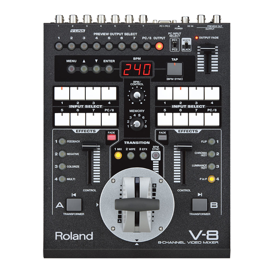
Page 4: Location Of Controsls
Mar. 2008 Location of Controsls fig.panel.eps_60... -
Page 5: Location Of Controls Parts List
Mar. 2008 Location of Controls Parts List Part Code Parts Name Description Q'ty 02450201 Y C-KEYTOP MX4H CLR 01787045 LED (ORANGE) SLR-325DCT31 02781634 TACT SWITCH SKRGAED010 02450190 Y C-KEYTOP MX1H CLR 01787045 LED (ORANGE) SLR-325DCT31 02781634 TACT SWITCH SKRGAED010 04903634 SLIDE SWITCH SSSU012200 00785856 LED (RED) -
Page 6: Exploded View
Mar. 2008 Exploded View fig.bunkaizu.eps@L... -
Page 7: Important Notes When Replacing The T-Bar
Mar. 2008 fig.bunkaizu.eps@R Important Notes When Replacing the T-Bar The T-bar Assembly (#71789367) is available as an older type (1-A in the When replacing the older-type T-bar Assembly (1-A) with the new type (1-B), figure) and a new type (1-B). The older type has a back fitting attached. be sure to also replace the older-type Shield Cover (11-A) with the new type Similarly, the Shield Cover (#05121512) is also available as an older type (11-A) (11-B). -
Page 8: Exploded View Parts List
Mar. 2008 Exploded View Parts List Part Code Part Name Description Q'ty ******** T-BAR ASSY Serial No.: Å`ZW90699 71789367 T-BAR ASSY Serial No.: ZX00700Å` 73895601 SCAN CNV BOARD ASSY 73895645 MAIN BOARD ASSY 73895656 T-BAR PANEL ASSY 03565234 J R-KNOB SF-ELA BLK/SLV 04903423 BOARD ANGLE... - Page 9 Mar. 2008...
-
Page 10: Block Diagram/Wiring Diagram
Mar. 2008 Block Diagram/Wiring Diagram fig.block-wiring.eps@L... - Page 11 Mar. 2008 fig.block-wiring.eps@R...
-
Page 12: Wiring Parts List
Mar. 2008 Wiring Parts List Part Code Part Name Connection Type Q'ty 05010601 WIRING WH 6X150-PHR-SAN-S WIRE 05010590 WIRING WH 10X200-PHR-SAN WIRE 04120545 WIRING 2X100-P2.5-XHP-SCN WIRE 05010578 WIRING WH 8X90-PHR-SAN-S WIRE 05010612 WIRING WH 4X150-PHR-SAN-S WIRE 05010712 WIRING WH 8X200-XHP-SCN WIRE 05010589 WIRING... -
Page 13: Parts List
Mar. 2008 Parts List fig.-part1-e.eps Due to one or more of the following reasons, SAFETY PRECAUTIONS: parts with parts code ******** cannot be supplied as service parts. The parts marked have safety-related characteristics. Use only listed parts for replacement. • Part supplied only as a component in a complete assembly •... - Page 14 Mar. 2008 DIODE 00785856 LED (RED) SLR-342VR3F 00348490 LED (RED) SLR-325VCT31 01787045 LED (ORANGE) SLR-325DCT31 04907256 LED SLR-325YCT31 POTENTIOMETER 02455223 9M/M ROTARY POTENTIOM- EVUF2KFK4B14 ETER 04232023 ROTARY POT. RK09Y11L0002 04903856 SLIDE POT. RS30111A4019 03898578 SLIDE POT. RS4511SA4A02 INDUCTORÅACOILÅAFILTER 04564812 CHOKE COIL SC-02-20G 12449347 FERRITE-BEAD...
- Page 15 Mar. 2008 ACCESSORIESÅiStandardÅj 04236101 AC ADAPTOR WITHOUT AC PSB-1U(S) UNIVERSAL CORD 01903334 AC CORD SET PSE 100V 1.0M FOR PSB-1U 02562456 AC CORD SET 120V 1.0M (NON POLAR) 01903356 AC CORD SET 230V 1.0M FOR PSB 03785590 AC CORD SET SC-078-NA05 240VA 00905234 EURO CONVERTER PLUG...
-
Page 16: Verifying The Version Number
IDs for both are using the same setting. To set the device ID for the V-8, go to the MIDI Setup menu and make the setting for Device ID. * Under Utility, set Memory Protect to OFF. -
Page 17: How To Update The System
Starting the Test Program Hold down the [TRANSFORMER A], [1 MIX], and [TRANSFORMER B] Using a video cable, connect the PREVIEW OUT jack on the V-8 to the buttons at the same time and press the [POWER] switch. video input jack on a television monitor. - Page 18 Mar. 2008 01: Tbar SET Press each of the switches indicated below, and verify that the LED goes dark and the corresponding indication on the monitor flashes. Move the video fader toward A, then press the [Transformer A] button. MENU: MENU The value of A is set.
- Page 19 ] and select Master. 25. Verify that the picture that is input is displayed on the television monitor Verify that the V-8ís built-in color bar is displayed. connected to the OUTPUT jack. Hold down the [MENU] button and press the [ENTER] button.
- Page 20 The test is executed the moment the [ENTER] button is pressed. ] and select DecB-Inp3 [C] or INPUT SELECT B3. * During the test, the picture output from the V-8 is a black screen. 45. Input video to INPUT 3.
- Page 21 Mar. 2008...
-
Page 22: Circuit Board (Main Board: 1/2)
Mar. 2008 Circuit Board (Main Board: 1/2) fig.b-main-1.eps... -
Page 23: Circuit Board (Main Board: 2/2)
Mar. 2008 Circuit Board (Main Board: 2/2) fig.b-main-2.eps... -
Page 24: Circuit Diagram (Main Board: 1/6)
Mar. 2008 Circuit Diagram (Main Board: 1/6) fig.c-main-1.eps@L... - Page 25 Mar. 2008 fig.c-main-1.eps@R...
-
Page 26: Circuit Diagram (Main Board: 2/6)
Mar. 2008 Circuit Diagram (Main Board: 2/6) fig.c-main-2.eps@L... - Page 27 Mar. 2008 fig.c-main-2.eps@R...
-
Page 28: Circuit Diagram (Main Board: 3/6)
Mar. 2008 Circuit Diagram (Main Board: 3/6) fig.c-main-3.eps@L... - Page 29 Mar. 2008 fig.c-main-3.eps@R...
-
Page 30: Circuit Diagram (Main Board: 4/6)
Mar. 2008 Circuit Diagram (Main Board: 4/6) fig.c-main-4.eps@L... - Page 31 Mar. 2008 fig.c-main-4.eps@R...
-
Page 32: Circuit Diagram (Main Board: 5/6)
Mar. 2008 Circuit Diagram (Main Board: 5/6) fig.c-main-5.eps@L... - Page 33 Mar. 2008 fig.c-main-5.eps@R...
-
Page 34: Circuit Diagram (Main Board: 6/6)
Mar. 2008 Circuit Diagram (Main Board: 6/6) fig.c-main-6.eps@L... - Page 35 Mar. 2008 fig.c-main-6.eps@R...
-
Page 36: Circuit Board (Jack 1, Jack 2, Jack 3 Board: 1/2)
Mar. 2008 Circuit Board (Jack 1, Jack 2, Jack 3 Board: 1/2) fig.b-jack-1.eps_75... -
Page 37: Circuit Board (Jack 1, Jack 2, Jack 3 Board: 2/2)
Mar. 2008 Circuit Board (Jack 1, Jack 2, Jack 3 Board: 2/2) fig.b-jack-2.eps_75 * The print wiring board of the Jack 3 Board has two kinds of the old 0490356700 and the new 04903567 01, but the Jack 3 Board Assy (#73895567) on which parts have been mounted has the same circuits both. -
Page 38: Circuit Diagram (Jack 1 Board)
Mar. 2008 Circuit Diagram (Jack 1 Board) fig.c-jack-1.eps@L... - Page 39 Mar. 2008 fig.c-jack-1.eps@R...
-
Page 40: Circuit Diagram (Jack 2 Board)
Mar. 2008 Circuit Diagram (Jack 2 Board) fig.c-jack-2.eps@L... - Page 41 Mar. 2008 fig.c-jack-2.eps@R...
-
Page 42: Circuit Diagram (Jack 3 Board: 1/2)
Mar. 2008 Circuit Diagram (Jack 3 Board: 1/2) fig.c-jack-3-1.eps@L... - Page 43 Mar. 2008 fig.c-jack-3-1.eps@R...
-
Page 44: Circuit Diagram (Jack 3 Board: 2/2)
Mar. 2008 Circuit Diagram (Jack 3 Board: 2/2) fig.c-jack-3-2.eps@L... - Page 45 Mar. 2008 fig.c-jack-3-2.eps@R...
-
Page 46: Circuit Board (Panel Board: 1/2)
Mar. 2008 Circuit Board (Panel Board: 1/2) fig.b-panel-1.eps_80... -
Page 47: Circuit Board (Panel Board: 2/2)
Mar. 2008 Circuit Board (Panel Board: 2/2) fig.b-panel-2.eps_80... -
Page 48: Circuit Diagram (Panel Board)
Mar. 2008 Circuit Diagram (Panel Board) fig.c-panel.eps@L... - Page 49 Mar. 2008 fig.c-panel.eps@R...
-
Page 50: Circuit Board (Scan Cnv Board: 1/2)
Mar. 2008 Circuit Board (Scan Cnv Board: 1/2) fig.b-scan-1.eps Circuit Board (Scan Cnv Board: 2/2) fig.b-scan-2.eps... - Page 51 Mar. 2008...
-
Page 52: Circuit Diagram (Scan Cnv Board)
Mar. 2008 Circuit Diagram (Scan Cnv Board) fig.c-scan.eps@L... - Page 53 Mar. 2008 fig.c-scan.eps@R...
- Page 54 Mar. 2008...