Sharp HT-DV40H Service Manual
Dvd cinema
Hide thumbs
Also See for HT-DV40H:
- Operation manual (68 pages) ,
- Quick start manual (2 pages) ,
- Operation manual (81 pages)
Table of Contents
Advertisement
Quick Links
[1]
Safety Precaution For Service Manual ......... 1-1
[2]
AC Power Supply Cord .......................... . ....... 1-2
[3]
Specifications ................................................ 1-2
[4]
Names Of Parts ............................................
[1]
Servo Section ............................................... 2-1
[2]
Test Mode ..................................................... 2-2
[3]
DVD Test Mode............................................. 2-3
[4]
DVD Firmware Update Test Mode ................ 2-4
CHAPTER 3. MECHANISM BLOCKS
[1]
Caution On Disassembly ....................... . ....... 3-1
[2]
Removing And Reinstalling The Main Parts . 3-4
[1]
Main Block Diagrams ............................. . ....... 4-1
[2]
DVD/CD Block Diagrams .............................. 4-3
[3]
Power Block Diagrams .......................... . ....... 4-5
Parts marked with "
" are important for maintaining the safety of the set. Be sure to replace these parts with specified
ones for maintaining the safety and performance of the set.
SHARP CORPORATION
SERVICE MANUAL
MODEL
[ Australia, Central & South America, Indonesia,
Singapore-Export/Vietnam, Middle East/Africa ]
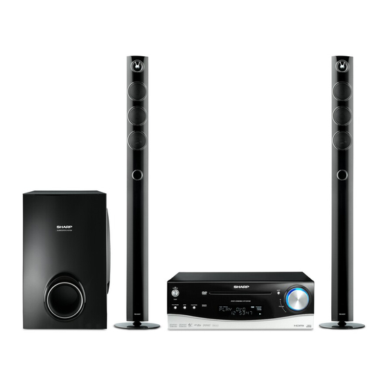
HT-DV40H DVD Cinema consisting of HT-DV40H
(main unit), CP-DV40H (front speaker) and
CP-SW40H (subwoofer system).
• In the interests of user-safety (Required by safety regulations in
some countries) the set should be restored to its original
condition and only parts identical to those specified be used.
CONTENTS
[1]
Waveforms Of DVD/CD Circuit...................... 5-1
[2]
Voltage .......................................................... 5-2
........ 1-4
[1]
Notes On Schematic Diagram....................... 6-1
[2]
Types Of Transistor And LED........................ 6-1
[3]
Schematic Diagram ....................................... 6-2
[4]
Wiring Side Of PWB .................................... 6-12
[1]
Troubleshooting............................................. 7-1
[1]
Function Table Of IC...................................... 8-1
[2]
FL Display ..................................................... 8-8
PARTS GUIDE
No. SY756HTDV40HW
DVD CINEMA
HT-DV40H
This document has been published to be used
for after sales service only.
The contents are subject to change without notice.
HT-DV40H
Advertisement
Table of Contents

Related Manuals for Sharp HT-DV40H


Summary of Contents for Sharp HT-DV40H
-
Page 1: Table Of Contents
HT-DV40H MODEL [ Australia, Central & South America, Indonesia, Singapore-Export/Vietnam, Middle East/Africa ] HT-DV40H DVD Cinema consisting of HT-DV40H (main unit), CP-DV40H (front speaker) and CP-SW40H (subwoofer system). • In the interests of user-safety (Required by safety regulations in some countries) the set should be restored to its original condition and only parts identical to those specified be used. -
Page 2: Precautions For Using Lead-Free Solder
HT-DV40H Audio XL-MP150 Service Manual XLMP150 Market PRECAUTIONS FOR USING LEAD-FREE SOLDER 1. Employing lead-free solder "MAIN, POWER, DISPLAY, SCART, VIDEO OUT, DIGITAL IN, DVD, SUBWOOFER PWB" of this model employs lead-free solder. The LF symbol indicates lead-free solder, and is attached on the PWB and service manuals. The alphabetical character following LF shows the type of lead-free solder. -
Page 3: Chapter 1. General Description
HT-DV40H CHAPTER 1: GENERAL DESCRIPTION [1] Safety Precaution For Service Manual WARNINGS THE AEL (ACCESSIBLE EMISSION LEVEL) OF LASER POWER OUTPUT FOR THIS MODEL IS SPECIFIED TO BE LOWER THAN CLASS I REQUIREMENTS. HOWEVER, THE FOLLOWING PRECAUTIONS MUST BE OBSERVED DURING SERVICING TO PROTECT YOUR EYES AGAINTS EXPOSURE TO THE LASER BEAM. -
Page 4: Specifications
HT-DV40H [3] Specifications HT-DV40H except Australia Main Unit Power source AC 220 - 240 V ~ 50 Hz USB host Complies with USB 1.1/2.0 (Full Speed) interface Mass-Storage-Class. Power Power on: 82 W Support Bulk only and CBI protocol. consumption Power stand-by: 0.6 W (*) - Page 5 HT-DV40H HT-DV40H for Australia Main Unit USB host Complies with USB 1.1/2.0 (Full Speed) Power source AC 220 - 240 V ~ 50 Hz interface Mass-Storage-Class. Power Power on: 82 W Support Bulk only and CBI protocol. consumption Power stand-by: 0.6 W (*)
-
Page 6: Names Of Parts
HT-DV40H [4] Names Of Parts Front panel 1. CD Compartment 2. On/Stand-by Button 3. Timer Indicator 4. DVD/CD/USB Play/Pause Button 5. Disc or USB Stop Button 6. Function Button 4 5 6 7 7. Remote Sensor 8. Headphone Socket 9. Disc Open/Close Button 10. - Page 7 HT-DV40H Remote control 1. Remote Control Transmitter 2. DVD Direct Button 3. DVD On Screen Button 4. Direct Search Buttons 5. Memory or Dimmer Button 6. DVD/CD/MP3/WMA Repeat Button 7. Menu Button 8. Enter Button 9. Cursor Left Button 10. DVD Chapter Skip/DVD/MP3/WMA Fast Reverse/CD/MP3/WMA Track Down/Tuner Preset Down and Time Down Button 11.
-
Page 8: Chapter 2. Adjustments
HT-DV40H CHAPTER 2. ADJUSTMENTS CD-ES700/CD-ES77 CD-ES700/CD-ES77 Service Manual CD-ES700/CD-ES77 Market [1] Servo Section • Adjustment Since this DVD system incorporates the following automatic adjustment functions, readjustment is not needed when replacing the pickup. Therefore, different PWBs and pickups can be combined freely. -
Page 9: Test Mode
HT-DV40H [2] Test Mode 1.Test Mode Functions 1.1.Entering the Test Mode While holding down both the n button and the ON/STAND-BY button of the main unit from the AC Supply Off state, turn the AC Supply ON to enter the Test Menu Mode. -
Page 10: Dvd Test Mode
HT-DV40H [3] DVD Test Mode At testmode menu, select "DVD TEST MODE" by [STEP 1] turning VOL Jog UP and Down and press [STOP] key to enter dvd test mode Note 1: [STEP 2] "DVD TEST", will appear in In dvd test mode, DVD start up in cd mode... -
Page 11: Dvd Firmware Update Test Mode
HT-DV40H [4] DVD Firmware Update Test Mode Note 1: After enter testmode menu, press [PLAY] key at main unit to select To enter testmode, during AC supply off "FW UPDATE TEST MODE" to condition, whilst pressing down STOP key and enter this mode ON/STAND-BY key together, turn ON AC Supply. - Page 12 HT-DV40H Amp abnormal detection and System PROTECTION display In case amp abnormal detection or System PROTECTION had occurred, the unit will automatically enter to stand-by mode and Timer indicator will flashing as below. Example : In case of amp abnormal...
- Page 13 HT-DV40H -MEMO- 2 – 6...
-
Page 14: Chapter 4. Diagrams
HT-DV40H CHAPTER 4. DIAGRAM [1] Main Block Diagrams (TP1) TO DVD PWB 1 2 3 4 Figure 4-1: MAIN BLOCK DIAGRAM (1/2) 4 – 1... - Page 15 HT-DV40H IC701 IXA161AW00 Figure 4-2: MAIN BLOCK DIAGRAM (2/2) 4 – 2...
-
Page 16: Dvd/Cd Block Diagrams
HT-DV40H [2] DVD/CD Block Diagrams Figure 4-3: DVD/CD BLOCK DIAGRAM (1/2) 4 – 3... - Page 17 HT-DV40H Power S.W. NJU7391 (2/2) Buffer 27,32 SCART SIGNAL Analog Signal Buffer 40, 41 OPT 1 SCART OPT 2 COAX Figure 4-4: DVD/CD BLOCK DIAGRAM (2/2) 4 – 4...
-
Page 18: Power Block Diagrams
HT-DV40H [3] Power Block Diagrams AC SUPPLY 220-240V ~ 50Hz Figure 4-5: POWER BLOCK DIAGRAM (1/2) 4 – 5... - Page 19 HT-DV40H Figure 4-6: POWER BLOCK DIAGRAM (2/2) 4 – 6...
-
Page 20: Chapter 5. Circuit Description
HT-DV40H CHAPTER 5. CIRCUIT DESCRIPTION [1] Waveform of CD / DVD Circuit VIDEO OUT S-VIDEO - Y OUTPUT S-VIDEO OUT - C OUT COMPONENT VIDEO OUT - Y Output (Interlace mode) COMPONENT VIDEO OUT - Y Output COMPONENT VIDEO OUT - Pb/Cb Output... - Page 21 HT-DV40H COMPONENT VIDEO OUT - Pb/Cb Output COMPONENT VIDEO OUT - Pr/Cr Output (P-Scan mode) (Interlace mode) WF10 WF11 COMPONENT VIDEO OUT - Pr/Cr Output Audio Left (P-Scan mode) WF12 WF13 Audio Right RF Signal (CD) WF14 RF Signal (DVD)
-
Page 22: Voltage
HT-DV40H [2] Voltage IC1 ( VHiSP8281AWU5 ) VOLTAGE VOLTAGE VOLTAGE VOLTAGE 1.65 3.26 1.99 3.52 1.67 3.26 3.27 3.24 0.93 1.63 1.30 0.00 2.07 1.63 1.27 0.00 2.09 0.00 3.12 3.43 2.06 0.00 3.00 3.85 2.06 4.34 2.97 3.34 2.06 3.26... - Page 23 HT-DV40H IC1 ( VHiSP8281AWU5 ) VOLTAGE VOLTAGE VOLTAGE VOLTAGE 1.55 1.46 0.61 3.11 0.00 2.00 0.63 0.24 0.00 1.18 0.04 2.41 0.00 1.22 2.96 1.09 2.88 3.18 0.00 0.87 1.70 3.10 1.50 2.21 1.08 1.49 1.51 2.20 2.03 1.93 1.51 0.79...
- Page 24 HT-DV40H IC6 ( VHiSPHE6500P- ) VOLTAGE VOLTAGE VOLTAGE VOLTAGE 0.00 0.00 0.00 0.00 1.64 0.00 3.24 0.00 4.23 0.00 3.24 3.75 0.09 0.00 0.00 1.79 4.20 0.00 3.77 0.03 0.05 0.00 3.77 3.26 3.24 0.00 3.25 2.82 4.24 0.00 3.48 1.48...
- Page 25 HT-DV40H IC11 ( VHiLC750512-1 ) VOLTAGE VOLTAGE VOLTAGE VOLTAGE 1.81 0.00 0.00 3.25 0.00 3.33 0.00 3.25 1.81 0.17 3.26 0.00 0.00 5.21 0.00 0.00 1.81 5.21 0.00 1.76 0.00 0.90 3.26 3.24 0.00 3.42 1.73 3.26 0.00 3.36 1.72 3.25...
- Page 26 HT-DV40H ( VSKTA1298Y/-1 ) ( VSKTA1298Y/-1 ) ( VSKTA1298Y/-1 ) ( VSKTC3875GR-1 ) VOLTAGE VOLTAGE VOLTAGE VOLTAGE 5.08 1.25 1.18 0.00 0.00 0.00 0.00 0.02 6.04 0.62 0.55 0.67 ( VS2SK536///-1 ) ( VS2SK536///-1 ) ( VSKTC3875GR-1 ) ( VSKTC3875GR-1 )
- Page 27 HT-DV40H IC 402 IC 502 VOLTAGE VOLTAGE VOLTAGE VOLTAGE 32.30 35.10 24.23 35.30 25.70 35.20 38.59 29.80 24.41 35.58 38.60 38.30 4.70 35.50 38.26 29.70 1.50 0.57 32.65 32.66 1.70 0.58 38.30 29.87 30.43 0.66 32.30 27.13 3.40 0.70 32.90 0.70...
- Page 28 HT-DV40H IC 701 VOLTAGE VOLTAGE VOLTAGE VOLTAGE 1.74 1.23 2.36 1.41 1.76 1.23 1.02 250.10m 0.94 1.24 0.99 226.50m 1.08 2.01 2.26 1.50 1.03 1.96 1.03 1.77 282.30m 1.19 1.05 1.99 0.94 1.18 1.07 1.90 0.94 1.18 258.50m 0.70 0.94 1.15...
- Page 29 HT-DV40H Q 804 Q 806 Q 807 QM 7 VOLTAGE VOLTAGE VOLTAGE VOLTAGE 2.70m 1.97 1.93 1.90 5.40 1.97 1.37 2.90m 23.40m 7.00 1.30 3.00m QM 8 QM 9 QM 16 QM 17 VOLTAGE VOLTAGE VOLTAGE VOLTAGE 3.40 2.68 8.55 0.76...
- Page 30 HT-DV40H -MEMO- 5 – 11...
-
Page 31: Chapter 6. Circuit Schematics And Parts Layout
HT-DV40H CHAPTER 6. CIRCUIT SCHEMATICS AND PARTS LAYOUT Audio CD-DV650W Service Manual CD-DV650W Market [1] Notes On Schematic Diagram • Schematic diagram and Wiring Side of P.W.Board for this model are subject to change for improvement without Resistor: • prior notice. -
Page 32: Schematic Diagram
HT-DV40H [3] Schematic Diagram AUDIO SIGNAL FM SIGNAL TO DISPLAY PWB-B2 TO DVD PWB-C MIC_IN Figure 6-1: MAIN SCHEMATIC DIAGRAM (1/8) 6 – 2... - Page 33 HT-DV40H DVD PWB-C (CNP14) 4700pF/ Figure 6-2: MAIN SCHEMATIC DIAGRAM (2/8) 6 – 3...
- Page 34 HT-DV40H SUBWOOFER PWB-D (BI402) Figure 6-3: MAIN SCHEMATIC DIAGRAM (3/8) 6 – 4...
- Page 35 HT-DV40H MIC_IN Figure 6-4: MAIN SCHEMATIC DIAGRAM (4/8) 6 – 5...
- Page 36 HT-DV40H AZ4558CME JP826 Figure 6-5: MAIN SCHEMATIC DIAGRAM (5/8) 6 – 6...
- Page 37 HT-DV40H C634 0.047/50V D605 MA111G D606 MA111G Figure 6-6: MAIN SCHEMATIC DIAGRAM (6/8) 6 – 7...
- Page 38 HT-DV40H AUDIO SIGNAL Figure 6-7: MAIN SCHEMATIC DIAGRAM (7/8) 6 – 8...
- Page 39 HT-DV40H SPEAKER TERMINAL Figure 6-8: MAIN SCHEMATIC DIAGRAM (8/8) 6 – 9...
- Page 40 HT-DV40H BI706 Figure 6-9: USB SCHEMATIC DIAGRAM 6 – 10...
- Page 41 HT-DV40H -MEMO- 6 – 11...
- Page 42 HT-DV40H 1.5K BLUE AC SUPPLY AC 220-240 V ~ 50Hz Figure 6-10: POWER SCHEMATIC DIAGRAM (1/2) 6 – 12...
- Page 43 HT-DV40H L912 F0015 R973 101P C999 HEADPHONE JACK Figure 6-11: POWER SCHEMATIC DIAGRAM (2/2) 6 – 13...
- Page 44 HT-DV40H Bi502 A691AW Figure 6-12: DISPLAY SCHEMATIC DIAGRAM (1/2) 6 – 14...
- Page 45 HT-DV40H Figure 6-13: DISPLAY SCHEMATIC DIAGRAM (2/2) 6 – 15...
- Page 46 HT-DV40H VIDEO SIGNAL CD SIGNAL SCART PWB-B3 DIGITAL-IN PWB-B5 VIDEO OUT PWB-B4 0.47uH FROM DVD PWB-C Figure 6-14: SCART, DIGITAL IN & VIDEO OUT SCHEMATIC DIAGRAM 6 – 16...
- Page 47 HT-DV40H -MEMO- 6 – 17...
- Page 48 HT-DV40H Figure 6-15: DVD SCHEMATIC DIAGRAM (1/8) 6 – 18...
- Page 49 HT-DV40H Figure 6-16: DVD SCHEMATIC DIAGRAM (2/8) 6 – 19...
- Page 50 HT-DV40H CD SIGNAL VIDEO SIGNAL TO SCART PWB-B3 Figure 6-17: DVD SCHEMATIC DIAGRAM (3/8) 6 – 20...
- Page 51 HT-DV40H TO MAIN PWB-A (CNS4) Figure 6-18: DVD SCHEMATIC DIAGRAM (4/8) 6 – 21...
- Page 52 HT-DV40H Figure 6-19: DVD SCHEMATIC DIAGRAM (5/8) 6 – 22...
- Page 53 HT-DV40H TO SCART PWB-B3 The number are waveform number shown in page 7-3 Figure 6-20: DVD SCHEMATIC DIAGRAM (6/8) 6 – 23...
- Page 54 HT-DV40H CD SIGNAL Figure 6-21: DVD SCHEMATIC DIAGRAM (7/8) 6 – 24...
- Page 55 HT-DV40H ILRCKA BICKA Figure 6-22: DVD SCHEMATIC DIAGRAM (8/8) 6 – 25...
- Page 56 HT-DV40H FROM MAIN PWB-A (BI402) Figure 6-23: SUBWOOFER SCHEMATIC DIAGRAM (1/2) 6 – 26...
- Page 57 HT-DV40H AUDIO SIGNAL SUBWOOFER SPEAKER OUTPUT TO MAIN PWB-A CNP801 Figure 6-24: SUBWOOFER SCHEMATIC DIAGRAM (2/2) 6 – 27...
- Page 58 HT-DV40H [4] Charts Of Connecting Wires (TP1) CNP901 Figure 6-25: WIRING CONNECTION (1/2) 6 – 28...
- Page 59 HT-DV40H CNS9 FROM DVD PWB-C CNS201 1 2 3 4 CNP201 1 2 3 4 RING CORE (2 TURN) RING CORE (2 TURN) CNS12 CNS201 VIDEO OUT PWB-B4 (CNP201) RING CORE (2 TURN) COLOR TABLE BLACK GREY YELLOW JK900 BROWN...
-
Page 60: Wiring Side Of Pwb
HT-DV40H [5] Wiring Side Of PWB MAIN PWB-A MICOM REFLASH ONLY 1 2 3 4 5 6 7 8 R-CH FRONT SPEAKERS TERMINAL L-CH Lead-free solder indication Lead-free solder is used in the MAIN PWB. Refer to "Precautions for handling lead-free solder" for instructions and precautions. - Page 61 HT-DV40H WIR2 (BL) B C E FROM USB EXTERNAL DEVICE COLOR TABLE BLUE Figure 6-28: WIRING SIDE OF MAIN PWB (TOP VIEW) (2/2) 6 – 31...
- Page 62 HT-DV40H MAIN PWB-A Lead-free solder indication Lead-free solder is used in the MAIN PWB. Refer to "Precautions for handling lead-free solder" for instructions and precautions. Figure 6-29: WIRING SIDE OF MAIN PWB (BOTTOM VIEW) (1/2) 6 – 32...
- Page 63 HT-DV40H COLOR TABLE BLUE GREY Figure 6-30: WIRING SIDE OF MAIN PWB (BOTTOM VIEW) (2/2) 6 – 33...
- Page 64 HT-DV40H POWER PWB-B1 AC POWER SUPPLY CORD (233) AC 220-240V~50Hz Lead-free solder indication Lead-free solder is used in the POWER PWB. Refer to "Precautions for handling lead-free solder" for instructions and precautions. Figure 6-31: WIRING SIDE OF POWER PWB (TOP VIEW) (1/2)
- Page 65 HT-DV40H 1 2 3 4 5 6 7 7 6 5 1 2 3 4 5 6 7 COLOR TABLE BROWN BLUE Figure 6-32: WIRING SIDE OF POWER PWB (TOP VIEW) (2/2) 6 – 35...
- Page 66 HT-DV40H POWER PWB-B1 Lead-free solder indication Lead-free solder is used in the POWER PWB. Refer to "Precautions for handling lead-free solder" for instructions and precautions. Figure 6-33: WIRING SIDE OF POWER PWB (BOTTOM VIEW) (1/2) 6 – 36...
- Page 67 HT-DV40H Figure 6-34: WIRING SIDE OF POWER PWB (BOTTOM VIEW) (2/2) 6 – 37...
- Page 68 HT-DV40H DISPLAY PWB-B2 1 2 3 4 1 2 3 4 5 6 7 8 9 10 11 12 13 14 15 16 17 18 19 20 21 22 23 24 25 26 27 28 30 31 Lead-free solder indication Lead-free solder is used in the DISPLAY PWB.
- Page 69 HT-DV40H 2 4 6 8 10 12 14 1 3 5 7 9 11 13 15 27 28 30 31 32 33 34 35 36 37 38 39 40 41 42 43 44 45 46 4748 49 50 51 Figure 6-36: WIRING SIDE OF DISPLAY PWB (TOP VIEW) (2/2)
- Page 70 HT-DV40H DISPLAY PWB-B2 Lead-free solder indication Lead-free solder is used in the DISPLAY PWB. Refer to "Precautions for handling lead-free solder" for instructions and precautions. Figure 6-37: WIRING SIDE OF DISPLAY PWB (BOTTOM VIEW) (1/2) 6 – 40...
- Page 71 HT-DV40H Figure 6-38: WIRING SIDE OF DISPLAY PWB (BOTTOM VIEW) (2/2) 6 – 41...
- Page 72 HT-DV40H SCART PWB-B3 SCART OUT AUDIO/VIDEO VIDEO OUT PWB-B4 DIGITAL IN PWB-B5 VIDEO COMPONENT S-VIDEO Lead-free solder indication Lead-free solder is used in the SCART, VIDEO OUT, DIGITAL IN PWB. Refer to "Precautions for handling lead-free solder" for instructions and precautions.
- Page 73 HT-DV40H SCART PWB-B3 VIDEO OUT PWB-B4 DIGITAL IN PWB-B5 Lead-free solder indication Lead-free solder is used in the SCART, VIDEO OUT, DIGITAL IN PWB. Refer to "Precautions for handling lead-free solder" for instructions and precautions. Figure 6-40: WIRING SIDE OF SCART, VIDEO OUT, DIGITAL IN PWB (BOTTOM VIEW)
- Page 74 HT-DV40H DVD PWB-C HDMI OUT Lead-free solder indication Lead-free solder is used in the DVD PWB. Refer to "Precautions for handling lead-free solder" for instructions and precautions. Figure 6-41: WIRING SIDE OF DVD PWB (TOP VIEW) (1/2) 6 – 44...
- Page 75 HT-DV40H COLOR TABLE GREEN BLACK BLUE Figure 6-42: WIRING SIDE OF DVD PWB (TOP VIEW) (2/2) 6 – 45...
- Page 76 HT-DV40H DVD PWB-C 20mm 10mm Filament tape Lead-free solder indication Lead-free solder is used in the DVD PWB. Refer to "Precautions for handling lead-free solder" for instructions and precautions. Figure 6-43: WIRING SIDE OF DVD PWB (BOTTOM VIEW) (1/2) 6 – 46...
- Page 77 HT-DV40H COPPER FOIL PSH3 20mm 10mm Filament tape COLOR TABLE GREEN BLACK BLUE Figure 6-44: WIRING SIDE OF DVD PWB (BOTTOM VIEW) (2/2) 6 – 47...
- Page 78 HT-DV40H SUBWOOFER PWB-D BI403 R405 L402 SUBWOOFER TERMINAL C406 C409 R414 C451 Lead-free solder indication Lead-free solder is used in the SUBWOOFER PWB. Refer to "Precautions for handling lead-free solder" for instructions and precautions. Figure 6-45: WIRING SIDE OF SUBWOOFER PWB (TOP VIEW) (1/2)
- Page 79 HT-DV40H R402 R420 L401 R421 BI402 R401 C417 R418 IC402 C433 C429 C403 C407 C422 R411 C431 R412 94V-0 Figure 6-46: WIRING SIDE OF SUBWOOFER PWB (TOP VIEW) (2/2) 6 – 49...
- Page 80 HT-DV40H SUBWOOFER PWB-D R429 R408 R415 C446 R425 R427 C464 C452 R407 R413 C455 C453 R423 C411 C441 Lead-free solder indication Lead-free solder is used in the SUBWOOFER PWB. Refer to "Precautions for handling lead-free solder" for instructions and precautions.
- Page 81 HT-DV40H C425 C460 C461 Q405 C424 D402 C432 D401 Figure 6-48: WIRING SIDE OF SUBWOOFER PWB (BOTTOM VIEW) (2/2) 6 – 51...
-
Page 82: Chapter 7. Flowchart
HT-DV40H CHAPTER 7. FLOWCHART [1] Troubleshooting 1. When the CD/DVD does not function The CD/DVD section may not operate when the objective lens of the optical pickup is dirty. Clean the objective lens, and check the playback operation. When this section does not operate even after the above step is taken, check the following items. - Page 83 HT-DV40H From 7-1 Page Is SLED control signal output from pin 58 of IC1 to pin 23 of IC2? Check SLED control signal line between IC1 and IC2 (Refer Figure 1) Is SPIN control signal output from pin 57 of IC1 to pin 4 of IC2?
- Page 84 HT-DV40H 3. Both Video and Audio do not operate normally The RF waveform is normal and the time is displayed normally, but no sound is produced. Or the sound has dropouts. 1. Insert disc into DISC loader. 2. When playback starts does the disc initialise ? Repeat steps as Focus Errror system check occurred.
- Page 85 HT-DV40H 4. Video is not output normally Put a disc on the DISC tray. Are the video signals input to the pins of CNP8 as shown below? Check the line between video out section and pins of CNP8 and CNP9.
-
Page 86: Chapter 8. Others
HT-DV40H CHAPTER 8. OTHERS [1] Function Table of IC IC1 VHISP8281AWU5 : DVD DECODER (SP8281) (1/3) BLOCK DIAGRAM Bootstrap PLLv PLLa Servo loader inf. Control Power control EPROM/ SRAM EPROM/SRAM RISC loader RF input interface Intr. control icache dcache Timer Graphics USB 1.1... - Page 87 HT-DV40H IC1 VHISP8281AWU5 : DVD DECODER (SP8281) (2/3) PIN CONFIGURATION A_DATA4/GPIO M_D10 A_IEC_RX/GPIO M_D11 A_IEC_TX/GPIO M_D12 A_DATA0/GPIO VDD_K2 VDD_O5 M_D13 A_DATA1/GPIO M_D14 A_DATA2/GPIO M_D15 A_DATA3/GPIO M_BA0 A_LRCK/GPIO M_CS0_B/GPIO VSS_K6/VSS_O6 VSS_O2/VSS_K2 A_BCK/GPIO M_RAS_B A_XCK/GPIO M_CAS_B UA0_RX/GPIO M_WE_B UA0_TX/GPIO M_D0 V_COMP M_D1...
- Page 88 HT-DV40H IC1 VHiSP8281AWU5 : DVD DECODER (SP8281) (3/3) PIN DESCRIPTION Symbol Pin # Input/Output Description VSS_O0/VSS_K0 Chip kernel logic and output shared ground pin #0 VSS_O1/VSS_K1 (#1) VSS_O2/VSS_K2 (#2) VSS_O2/VSS_K3 (#3) VSS_O2/VSS_K4 (#4) VSS_O2/VSS_K5 (#5) VSS_O2/VSS_K6 (#6) VSS_O2/VSS_K7 (#7) VDD_K0...
- Page 89 HT-DV40H Symbol Pin # Input/Output Description SPDC_OUT/ Input/Output Servo SPDC_OUT GPIO Priority selection Function GPIO[66] Input/Output gpio_first[4][2] = 1 AT_RESET_B Output sft_cfg13[11:9] = 3'b001 AT_ADR[2] Output sft_cfg13[11:9] = 3'b111 AT_D[1] Input/Output sft_cfg13[14:12] = 3'b011 AT_D[1] Input/Output sft_cfg13[14:12] = 3'b101 AT_D[1]...
- Page 90 HT-DV40H Symbol Pin # Input/Output Description TRAY_OUT/ Input/Output Servo TRAY_OUT GPIO Priority selection Function GPIO[69] Input/Output gpio_first[4][5] = 1 AT_IORDY_B Input sft_cfg13[11:9] = 3'b001 AT_D[13] Input/Output sft_cfg13[14:12] = 3'b011 AT_D[13] Input/Output sft_cfg13[14:12] = 3'b101 AT_D[13] Input/Output sft_cfg13[14:12] = 3'b110 TRAY_OUT (default)
- Page 91 HT-DV40H Symbol Pin # Input/Output Description HOMESW/GPIO Input/Output Servo HOMESW Priority selection Function GPIO[6] Input/Output gpio_first[0][6] = 1 ADC_DATA Input sft_cfg13[8:4] = 5'b00010 UA0_RXD Input sft_cfg2[3:2] = 2 AT_CS_B[1] Output sft_cfg13[11:9] = 3'b001 AT_ADR[0] Output sft_cfg13[11:9] = 3'b010 AT_D[4] Input/Output...
- Page 92 HT-DV40H Symbol Pin # Input/Output Description DFCT/GPIO Input/Output Servo DFCT Priority selection Function GPIO[8] Input/Output gpio_first[0][8] = 1 IEC_RX Input sft_cfg13[3:0] = 4'b0101 AT_INTRQ Input sft_cfg13[11:9] = 3'b001 AT_CS_B[0] Output sft_cfg13[11:9] = 3'b010 AT_INTRQ Input sft_cfg13[11:9] = 3'b100 AT_D[5] Input/Output...
- Page 93 HT-DV40H Symbol Pin # Input/Output Description GPIO/ Input/Output GPIO TRAY_IS_OUT Priority selection Function Input/Output GPIO[10] gpio_first[0][10] = 1 Output UA0_RTS_B sft_cfg2[7:6] = 3 Output AT_CS_B[1] sft_cfg13[11:9] = 3'b100 Input/Output AT_D[0] sft_cfg13[14:12] = 3'b010 Input/Output AT_D[6] sft_cfg13[14:12] = 3'b011 Input/Output sft_cfg13[14:12] = 3'b101...
- Page 94 HT-DV40H Symbol Pin # Input/Output Description GPIO Input/Output GPIO Priority selection Function Input/Output gpio_first[0][12] = 1 GPIO[12] Output sft_cfg2[7:6] = 3 UA0_DTR_B Output sft_cfg13[11:9] = 3'b100 AT_ADR[2] Input/Output sft_cfg13[14:12] = 3'b010 AT_D[1] Input/Output sft_cfg13[14:12] = 3'b011 AT_D[7] Input/Output sft_cfg13[14:12] = 3'b101...
- Page 95 HT-DV40H Symbol Pin # Input/Output Description GPIO Input/Output GPIO Priority selection Function gpio_first[0][14] = 1 GPIO[14] Input/Output UA0_DCD_B sft_cfg2[7:6] = 3 Input AT_RESET_B sft_cfg13[11:9] = 3'b011 Output AT_IORDY_B sft_cfg13[11:9] = 3'b100 Input AT_RESET_B sft_cfg13[11:9] = 3'b101 Output AT_RESET_B sft_cfg13[11:9] = 3'b110...
- Page 96 HT-DV40H Symbol Pin # Input/Output Description R_CS4_B/GPIO Input/Output ROM / SRAM / flash chip select #4 or GPIO Priority selection Function Input/Output gpio_first[1][0] = 1 GPIO[16] Output sft_cfg1[3] = 1'b1 R_CS4_B (default) Input sft_cfg13[3:0] = 4'b0111 IEC_RX Input sft_cfg13[8:4] = 5'b00110...
- Page 97 HT-DV40H Symbol Pin # Input/Output Description R_A19 Input/Output ROM / SRAM / flash address bus bit [19] Priority selection Function Input/Output gpio_first[4][9] = 1 GPIO[73] ROM_ADDR[19](default) Input/Output PINMUX_control[0][0] = 1 Input sft_cfg1[11:9] = 3'b110 NT1_11 Input/Output sfg_cfg16[15:12] = 4'b1000 FM_GPIOB[15]...
- Page 98 HT-DV40H Symbol Pin # Input/Output Description M_A[6] Input/Output SDRAM address bus [6] M_A[5] Input/Output SDRAM address bus [5] M_A[4] Input/Output SDRAM address bus [4] M_DQM1/GPIO Input/Output SDRAM data input/output mask for M_DD[15:8], or GPIOA[27] Priority selection Function SDRAM data input/output Input/Output sft_cfg0[3]=1íb1...
- Page 99 HT-DV40H Symbol Pin # Input/Output Description GPIO/M_DD[29] Input/Output SDRAM data bus bit 29 or GPIO[32] Priority selection Function Input/Output hw_cfg_chg[5]=1íb1 SDRAM data bus [29] Input/Output gpio_first[2][0] = 1 GPIO[32] Input/Output hw_cfg_chg[4] = 1'b1 FL_ROM_DATA[13] Input sft_cfg2[7:6] = 1 UA0_CTS_B Input/Output...
- Page 100 HT-DV40H Symbol Pin # Input/Output Description GPIO/M_DD[26] Input/Output SDRAM data bus bit 26 or GPIO[35] Priority selection Function Input/Output hw_cfg_chg[5]=1íb1 SDRAM data bus [26] Input/Output gpio_first[2][3] = 1 GPIO[35] Input/Output hw_cfg_chg[4] = 1'b1 FL_ROM_DATA[10] Output sft_cfg2[7:6] = 1 UA0_DTR_B Input/Output...
- Page 101 HT-DV40H Symbol Pin # Input/Output Description M_DQM3/GPIO Input/Output SDRAM data input/output mask for M_DD[31:24] , or GPIO[38] Priority selection Function SDRAM data input/output Output sft_cfg0[5]=1’b1 mask for M_DD[31:24] (default) gpio_first[2][6] = 1 GPIO[38] Input/Output sft_cfg13[3:0] = 4'b1011 IEC_RX Input Input...
- Page 102 HT-DV40H Symbol Pin # Input/Output Description GPIO/M_DD[22] Input/Output GPIO[41] or SDRAM data bus bit 22 Priority selection Function hw_cfg_chg[5]=1’b1 SDRAM data bus [22] Input/Output gpio_first[2][9] = 1 GPIO[41] Input/Output sft_cfg0[5] = 1'b1 SD_FF_HWORD_UDQM Output sft_cfg13[14:12] = 3'b001 AT_D[4] Input/Output AT_D[4]...
- Page 103 HT-DV40H Symbol Pin # Input/Output Description GPIO/M_DD[20] Input/Output GPIO[43] or SDRAM data bus bit 20 Priority selection Function hw_cfg_chg[5]=1’b1 SDRAM data bus [20] Input/Output gpio_first[2][11] = 1 GPIO[43] Input/Output sft_cfg13[14:12] = 3'b001 AT_D[5] Input/Output sft_cfg13[14:12] = 3'b100 AT_D[5] Input/Output {sft_cfg20[0],sft_cfg7[5:4]} =...
- Page 104 HT-DV40H Symbol Pin # Input/Output Description GPIO/M_DD[18] Input/Output GPIO[45] or SDRAM data bus bit 18 Priority selection Function hw_cfg_chg[5]=1’b1 SDRAM data bus [18] Input/Output gpio_first[2][13] = 1 GPIO[45] Input/Output sft_cfg13[14:12] = 3'b001 AT_D[6] Input/Output sft_cfg13[14:12] = 3'b100 AT_D[6] Input/Output {sft_cfg20[0],sft_cfg7[5:4]} =...
- Page 105 HT-DV40H Symbol Pin # Input/Output Description GPIO/M_DD[16] Input/Output GPIO[47] or SDRAM data bus bit 16 Priority selection Function hw_cfg_chg[5]=1’b1 SDRAM data bus [16] Input/Output gpio_first[2][15] = 1 GPIO[47] Input/Output sft_cfg13[8:4] = 5'b01110 ADC_DATA Input sft_cfg13[11:9] = 3'b100 AT_RESET_B Output sft_cfg13[14:12] = 3'b001...
- Page 106 HT-DV40H Symbol Pin # Input/Output Description M_A[12]/GPIO Input/Output SDRAM address bus [12] or GPIO[49] Priority selection Function SDRAM address bus [12] Output sft_cfg1[5]=1’b1 (default) gpio_first[3][1] = 1 GPIO[49] Input/Output sft_cfg13[3:0] = 4'b1100 IEC_RX Input sft_cfg13[8:4] = 5'b10000 ADC_DATA Input sft_cfg13[11:9] = 3'b100...
- Page 107 HT-DV40H Symbol Pin # Input/Output Description AIN_R ADC input (right channel) (8202A only) GPIO Input/Output GPIO (8202A-256 only) Priority selection Function Input/Output gpio_first[6][7] = 1 GPIO[103] sft_cfg13[3:0] = 4'b1111 IEC_RX Input sft_cfg13[8:4] = 5'b11101 ADC_DATA Input sft_cfg13[14:12] = 3'b111 AT_D[8]...
- Page 108 HT-DV40H Symbol Pin # Input/Output Description A_IEC_TX/GPIO Input/Output IEC-958 transmit data Priority selection Function gpio_first[3][4] = 1 GPIO[52] Input/Output sft_cfg3[8] = 1'b1 IEC_TX (default) Output (other) GPIO[52] Input/Output A_DATA[0] / Input/Output Serial audio data output for channel 1/0 or GPIO...
- Page 109 HT-DV40H Symbol Pin # Input/Output Description UA0_TX/GPIO Input/Output UART #0 data transmit or GPIO Priority selection Function gpio_first[3][13] = 1 GPIO[61] Input/Output sft_cfg2[3:2] = 1 UA0_TXD (default) Input sft_cfg3[13:12] = 1 TV_VSYNC Input/Output sft_cfg14[10:8] = 3'b011 TV_VDSYNC_SRGB Output sft_cfg4[15:13] = 3'b011...
- Page 110 HT-DV40H Symbol Pin # Input/Output Description R_A22/GPIO Input/Output ROM / SRAM / flash address bus bit [22], or GPIO[94] Priority selection Function GPIO[94] Input/Output gpio_first[5][14] = 1 ROM_ADDR[22] (default)B Input/Output PINMUX_control[0][3] = 1 {sft_cfg20[0],sft_cfg7[5:4]} = 3'b010 656_DATA[5] Output {sft_cfg20[1],sft_cfg19[5:4]} = 3'b010 HD_DATA[5]...
- Page 111 HT-DV40H Symbol Pin # Input/Output Description GPIO Input/Output GPIO[98] Priority selection Function GPIO[98] Input/Output gpio_first[6][2] = 1 {sft_cfg20[0],sft_cfg7[5:4]} = 3'b010 656_CLK Output {sft_cfg20[1],sft_cfg19[5:4]} = 3'b010 HD_VCLK Input {sft_cfg20[2],sft_cfg14[7:6]} = 3'b010 SRGB_DCLK Output TS_DATA[3] Input/Output sft_cfg11[8:6] = 3'b110 TV_LCD_B_EXT[0] Output sft_cfg11[11:9] = 3'b001...
- Page 112 HT-DV40H Symbol Pin # Input/Output Description AGCON Output Differential AGC output #N AGCOP Output Differential AGC output #P RFIP Input Differential RF signal input RFIS Input Single-ended RF equalizer input RFSUM Output RF summing amplified output DPDA Input DPDB Input...
- Page 113 HT-DV40H IC2 VHIAT5669H++1 : 5 CHANNEL MOTOR DRIVER (AT5669) (1/2 ) BLOCK DIAGRAM 8.5K MUTE STAND-BY 1_2_3_4 VCC1 VREF VBIAS 8.5K VREF VCC1 VCC2 CPIN 8.0K PGND 7.5K VCC1 Pre-DRV VCTL VCC1 CPIP OUT5- TRAY 18.75K DRIVER VCC2 VCC2 OUT5+...
- Page 114 HT-DV40H IC2 VHIAT5669H++1 : 5 CHANNEL MOTOR DRIVER (AT5669) (2/2 ) PIN DESCRIPTION Pin No. Pin name Function CH1(Focus coil) input Linear Regulator 3V3 driver output Linear Regulator 2 feedback input CH2(Sled driver) input Linear Regulator 3V3 input CH5 forward input...
- Page 115 HT-DV40H IC4 VHIEM638165-1 : 16 Bit, SDRAM ( EM638165 ) ( 1/2 ) BLOCK DIAGRAM CLOCK CLOCK BUFFER 1MX16 CELL ARRAY CONTROL (BANK #A) COMMAND RAS# SIGNAL DECODER CAS# Column Decoder GENERATOR UDQM LDQM COLUMN Buffer COUNTER DQ15 MODE REGISTER...
- Page 116 HT-DV40H IC4 VHIEM638165-1 : 16 Bit, SDRAM ( EM638165 ) ( 2/2 ) PIN CONFIGURATION DQ15 VDDQ VSSQ DQ14 DQ13 VSSQ VDDQ DQ12 DQ11 VDDQ VSSQ DQ10 VSSQ VDDQ NC/RFU LDQM UDQM CAS# RAS# A10/AP IC5 : FLASH ROM, 48 BIT ( EN29LV800B ) ( 1/2 )
- Page 117 HT-DV40H IC5 : FLASH ROM, 48 BIT ( EN29LV800B ) ( 2/2 ) *Note: Refer Parts Guide page 1 under item [1] INTEGRATED CIRCUITS PIN DESCRIPTION Pin No. Pin Name Function 1~9, 16~25 A0-A19 Addresses 29~36, 38~44 DQ0-DQ14 15 Data Inputs/Outputs...
- Page 118 HT-DV40H IC6 VHISPHE6500P- : HDMI TRANSMITTER, 128 Pin ( SPHE6500P ) ( 2/3 ) PIN CONFIGURATION 64 DVCC18 63 DGND 62 DVCC18 61 DGND DGND 60 DVCC33 59 DGND DGND 58 DVCC18 GPIO_2_0 57 DGND GPIO_2_1 56 DVCC18 GPIO_2_2 55 DGND...
- Page 119 HT-DV40H Mnemonic Pin# Type Dir. Description LVTTL RGB24 interface bit-12 (B[2]) or GPIO_1_12(CCIR656-like link) LVTTL RGB24 interface bit-13 (B[3]) or GPIO_1_13(CCIR656-like link) LVTTL RGB24 interface bit-14 (B[4]) or GPIO_1_14(CCIR656-like link) LVTTL RGB24 interface bit-15 (B[5]) or GPIO_1_15(CCIR656-like link) LVTTL Intput...
- Page 120 HT-DV40H Mnemonic Pin# Type Dir. Description HPVCC1 Power HDMI PLL1 power 3.3V HPVCC2 Power HDMI PLL2 power 3.3V TMDSVCC18 Power HDMI analog power 1.8V AVDD1 Power Video DAC power 3.3V AVSS1 Video DAC GND AVDD2 Power Video DAC power 3.3V...
- Page 121 HT-DV40H IC10 VHINJU26220FN : DOLBY VIRTUAL SPEAKER / HEADPHONE DECODER ( NJU26220FN ) ( 2/3 ) PIN CONFIGURATION TEST SDO2 TEST SDO1 SDO0 TEST VDDIO RESETb VSSIO VDDIO VSSIO NJU26220 CLKOUT SD13 SD12 SD11 SD10 VSSPLL VDDPLL Figure 8-6 BLOCK DIAGRAM OF IC...
- Page 122 HT-DV40H IC10 VHINJU26220FN : DOLBY VIRTUAL SPEAKER / HEADPHONE DECODER ( NJU26220FN ) ( 3/3 ) PIN DESCRIPTION Pin No. Symbol Input/Output Function 1,11,20,32,40 VDDIO I/O Power Supply +3.3V BCKI Input Bit Clock Input 3,10,19,31,41 VSSIO I/O GND 4,15,30,42 Core GND 5,16,29,43 Core Power Supply +1.8V...
- Page 123 HT-DV40H IC11 VHILC750512-1 : AUDIO ENHANCER ( LC750512 ) ( 1/2 ) PIN DESCRIPTION Pin No. Terminal Name Input / Output Function PLLPWRR Input Power ring for PLL (ESD) (+1.8 V). PLLGNDR — GND for PLL (ESD). PLLAVDD Input Power supply for PLL (+1.8 V).
- Page 124 HT-DV40H Pin No. Terminal Name Input / Output Function DVDD2 Input Digital power supply (+1.8V). PWDB Input Power down input (L-Active). RSTB Input Reset input (L-Active). INTB Input Interrupt input (“H” Fixed input). MCUIFSEL Input Microprocessor I/F (CCB: Low; I2C: High). Select input.
- Page 125 HT-DV40H IC13 VHIAK4683EQ-1 : MULTI CHANNEL AUDIO CODEC ( AK4683 ) ( 1/3 ) BLOCK DIAGRAM RMCLK Clock DAIF Input Recovery X’tal Decoder Selector Oscillator IPS0/1, OPS0/1 bit LISEL MCLK2 LOPIN LIN1 LIN2 MCKO LIN3 HPF, LIN4 Audio DVOL PORTB...
- Page 126 HT-DV40H IC13 VHIAK4683EQ-1 : MULTI CHANNEL AUDIO CODEC ( AK4683 ) ( 2/3 ) PIN CONFIGURATION 64 63 62 61 60 59 58 57 56 55 54 53 52 51 50 49 PVDD RISEL ROPIN LOPIN LISEL AVSS2 AVDD2 VCOM...
- Page 127 HT-DV40H IC13 VHIAK4683EQ-1 : MULTI CHANNEL AUDIO CODEC ( AK4683 ) ( 3/3 ) PIN DESCRIPTION Pin Name Input / Output Function PVDD — PLL Power supply Pin, 4.5V~5.5V Receiver Channel 0 Pin (Internal biased pin. Internally biased at Input PVDD/2) Control Mode Select Pin.
- Page 128 HT-DV40H Pin Name Input / Output Function ROPIN Output Rch Feedback Resistor Input Pin. 0.5 x AVDD1. RISEL Output Rch Feedback Resistor Output Pin AVSS1 — ADC Ground Pin, 0V AVDD1 — ADC Power Supply Pin, 4.5V~5.5V LIN1 Input Lch Input 1 Pin...
- Page 129 HT-DV40H IC701 RH-IXA161AW00 : SYSTEM MICRO COMPUTER ( IXA161AW00 ) ( 1/5 ) PIN CONFIGURATION P140 / PCBUZ0 DIR_SCL/AD_SCL/E P60 / SCL0 Mic IN / INTP6 NH SCL P141 / DIR_SDA/AD_SCA/E CCB CLK P61 / SDA0 PCLBUZ1 NH SDA P142 / SCK20 /...
- Page 130 HT-DV40H IC701 RH-IXA161AW00 : SYSTEM MICRO COMPUTER ( IXA161AW00 ) ( 2/5 ) PIN DESCRIPTION NAME Input / Output FORM FUNCTION OUTLINE PORT_TYPE DIR_SCL/AD_SCL/ENH_SC [I2Cbus] Micom IF Clock for DVS / Audistry Output P60/SCL0 control DIR_SDA/AD_SDA/ENH_SD [I2Cbus] Micom IF Data I/O for DVS/Audistry...
- Page 131 HT-DV40H IC701 RH-IXA161AW00 : System Microcomputer ( IXA161AW ) ( 3/5 ) NAME Input / Output FORM FUNCTION OUTLINE PORT_TYPE -20dB ATT -20db ATT circuit control CMOS INPUT / Output ON = H OUTPUT P85/EX5 AMP_MUTE AMP MUTE CONTROL CMOS INPUT /...
- Page 132 HT-DV40H IC701 RH-IXA161AW00 : System Microcomputer ( IXA161AW ) ( 4/5 ) NAME Input/ Output FORM FUNCTION OUTLINE PORT_TYPE Avss DVD PROTECT DVD power supply abnormal detect CMOS INPUT / Input Analog In OUTPUT P156/ANi14 PROTECT Gen power supply abnormal detect...
- Page 133 AMP PROTECT Power IC abnormal detect CMOS INPUT / Input Abnormal = L OUTPUT P120/INTP0/EXLVi RX IN CMOS INPUT / Input SHARP 15bit remocon receive OUTPUT P47/INTP2 P-IN CMOS INPUT / Input Power Fail detect OUTPUT P46/INTP1/Ti05/To05 FL DO CMOS INPUT /...
- Page 134 HT-DV40H [2] LCD Display FL501:VVKNV12MM61-1 GRID ASSIGNMENT TITLE FOLD PTYI CHAP TOTAL X-BASS DIGITAL co11 co13 MEMORY ANGLE co12 co14 (2G - 11G) ANODE CONNECTION FOLD FOLD DIGITAL TITLE TITLE CHAP CHAP SLEEP PTYI PTYI DAILY (left) TOTAL TOTAL (right)
- Page 135 MODEL Destination Table [ Australia, Central & South America, Indonesia, Australia Singapore-Export/Vietnam, Middle East/Africa ] Central & South America Egypt HT-DV40H DVD Cinema consisting of HT-DV40H Indonesia (main unit), CP-DV40H (front speaker) and Jordan CP-SW40H (subwoofer system). Kuwait Singapore-Export/Vietnam Syria...
- Page 136 HT-DV40H PRICE PART PARTS CODE DESCRIPTION RANK MARK RANK [1] INTEGRATED CIRCUITS DVD Decoder VHiSP8281AWU5 VHiAT5669H++1 5 Channel Motor Driver Voltage Regulator, 1.8V VHiKiA1117F18 16 Bit, SDRAM VHiEM638165-1 Flash ROM, 48 Bit [ for SE / SY / KW / EG / JO ]...
- Page 137 HT-DV40H PRICE PART PARTS CODE DESCRIPTION RANK MARK RANK [3] DIODES VHDMA111G++-1 Silicon,MA111 Silicon,MA111 VHDMA111G++-1 Silicon,MA111 D205 VHDMA111G++-1 Silicon,MA111 D206 VHDMA111G++-1 Silicon,HSS4148 D207 VHDHSS4148+-1 Silicon,HSS4148 D208 VHDHSS4148+-1 Silicon,MA111 D209 VHDMA111G++-1 Silicon,MA111 D210 VHDMA111G++-1 Silicon,KDS226 D402 VHDKDS226//-1 Silicon,MA111 D403 VHDMA111G++-1 Silicon,MA111...
- Page 138 HT-DV40H PRICE PART PARTS CODE DESCRIPTION RANK MARK RANK [5] COILS Coil RCILFA116WJZZ Coil RCILFA116WJZZ Coil RCILFA116WJZZ Coil RCILFA116WJZZ Coil, 1 µH VPBNN1R0K0000 Coil, 1 µH VPBNN1R0K0000 Coil, 1 µH VPBNN1R0K0000 Coil, 1 µH VPBNN1R0K0000 Coil, 2.7 µH L201 VPBNN2R7K0000 Coil, 1 µH...
- Page 139 HT-DV40H PRICE PART PARTS CODE DESCRIPTION RANK MARK RANK [7] CAPACITORS 270 pF,50V C060 VCKYCY1HB271K 270 pF,50V C061 VCKYCY1HB271K 270 pF,50V C062 VCKYCY1HB271K 270 pF,50V C063 VCKYCY1HB271K 100 µ F,16V,Electrolytic VCEAEA1CW107M 220 µ F,10V,Electrolytic VCEAEA1AW227M 0.1 µ F,16V VCKYCY1CB104K 0.1 µ F,16V VCKYCY1CB104K 0.1 µ...
- Page 140 HT-DV40H PRICE PART PARTS CODE DESCRIPTION RANK MARK RANK [7] CAPACITORS 0.1 µ F,16V VCKYCY1CB104K 0.1 µ F,16V VCKYCY1CB104K 0.1 µ F,16V VCKYCY1CB104K 0.1 µ F,16V VCKYCY1CB104K 0.1 µ F,16V VCKYCY1CB104K 1200 pF,50V C141 VCKYCY1HB122K 1200 pF,50V C142 VCKYCY1HB122K 1 µ F,25V...
- Page 141 HT-DV40H PRICE PART PARTS CODE DESCRIPTION RANK MARK RANK [7] CAPACITORS 0.001 µ F,50V C521 VCKYCY1HB102K 270 pF (CH),50V C525 VCCCCY1HH271J 0.47 µ F,50V,Electrolytic C526 VCEAZA1HW474M 82 pF (CH),50V C527 VCCCCY1HH820J 22 µ F,50V,Electrolytic C528 VCEAZA1HW226M 0.1 µ F,25V C529...
- Page 142 HT-DV40H PRICE PART PARTS CODE DESCRIPTION RANK MARK RANK [7] CAPACITORS 0.1 µ F,50V C832 VCKYTV1HB104K 220 pF (CH),50V C833 VCCCCY1HH221J 0.1 µ F,50V C834 VCKYCY1HB104K 0.1 µ F,50V C835 VCKYCY1HB104K 0.1 µ F,50V C836 VCKYTV1HB104K 0.1 µ F,63V,Mylar C837 VCFYFA1JA104J 0.1 µ...
- Page 143 HT-DV40H PRICE PART PARTS CODE DESCRIPTION RANK MARK RANK [7] CAPACITORS 2200 p F,AC250V C958 RC-KZA038WJZZ 0.47 F,AC275V C959 RC-FZA026WJZZ 0.47 F,AC275V C960 RC-FZA026WJZZ 0.47 F,AC275V C961 RC-FZA026WJZZ 2200 p F,AC250V C962 RC-KZA038WJZZ 220 µ F,35V C972 RC-EZ0159AWZZ 0.1 µ F,50V...
- Page 144 HT-DV40H PRICE PART PARTS CODE DESCRIPTION RANK MARK RANK [7] CAPACITORS 0.1 µ F,16V CA70 VCKYCY1CB104K 100 µ F,10V,Electrolytic CA71 VCEAEA1AW107M 0.1 µ F,16V CA72 VCKYCY1CB104K 100 µ F,10V,Electrolytic CA73 VCEAEA1AW107M 0.1 µ F,16V CA74 VCKYCY1CB104K 0.1 µ F,16V CA76 VCKYCY1CB104K 0.1 µ...
- Page 145 HT-DV40H PRICE PART PARTS CODE DESCRIPTION RANK MARK RANK [7] CAPACITORS 0.1 µ F,16V CB80 VCKYCY1CB104K 33 pF (CH),50V CB81 VCCCCY1HH330J 33 pF (CH),50V CB82 VCCCCY1HH330J 33 pF (CH),50V CB83 VCCCCY1HH330J 0.1 µ F,16V CB84 VCKYCY1CB104K 0.1 µ F,16V CB85 VCKYCY1CB104K 0.1 µ...
- Page 146 HT-DV40H PRICE PART PARTS CODE DESCRIPTION RANK MARK RANK [9] RESISTORS 1 kohms,1/16W CM19 VRS-CY1JB102J 0 ohms,Jumper,1.25x2mm VRS-TV2AB000J 0 ohms,Jumper,1.25x2mm VRS-TV2AB000J 0 ohms,Jumper,1.25x2mm JP701 VRS-TV2AB000J 0 ohms,Jumper,0.8x1.55mm JP801 VRS-CY1JB000J 0 ohms,Jumper,1.25x2mm JP807 VRS-TV2AB000J 0 ohms,Jumper,1.25x2mm JP810 VRS-TV2AB000J 0 ohms,Jumper,1.25x2mm JP812 VRS-TV2AB000J 0 ohms,Jumper,0.8x1.55mm...
- Page 147 HT-DV40H PRICE PART PARTS CODE DESCRIPTION RANK MARK RANK [9] RESISTORS 0 ohms,Jumper,1.25x2mm VRS-TV2AB000J 33 ohms,1/16W VRS-CY1JB330J 0 ohms,Jumper,1.25x2mm R146 VRS-TV2AB000J 0 ohms,Jumper,1.25x2mm R147 VRS-TV2AB000J 10 kohms,1/16W R151 VRS-CY1JB103J 10 kohms,1/16W R152 VRS-CY1JB103J 100 kohms,1/16W R161 VRS-CY1JB104J 100 kohms,1/16W R164 VRS-CY1JB104J 4.7 kohms,1/16W...
- Page 148 HT-DV40H PRICE PART PARTS CODE DESCRIPTION RANK MARK RANK [9] RESISTORS 4.7 kohms,1/16W R661 VRS-CY1JB472J 220 ohms,1/16W R670 VRS-CY1JB221J 220 ohms,1/16W R671 VRS-CY1JB221J 6.8 kohms,1/16W R672 VRS-CY1JB682J 6.8 kohms,1/16W R673 VRS-CY1JB682J 1 kohms,1/16W R674 VRS-CY1JB102J 1 kohms,1/16W R675 VRS-CY1JB102J 0 ohms,Jumper,0.8x1.55mm...
- Page 149 HT-DV40H PRICE PART PARTS CODE DESCRIPTION RANK MARK RANK [9] RESISTORS 10 ohms,1/10W R813 VRS-TV2AB100J 22 ohms,5W R814 VRN-CM05N220J 1 Mohms,1/16W R816 VRS-CY1JB105J 1 Mohms,1/16W R817 VRS-CY1JB105J 100 kohms,1/16W R818 VRS-CY1JB104J 100 kohms,1/16W R819 VRS-CY1JB104J 10 kohms,1W R820 VRS-VV3AA103J 10 kohms,1W...
- Page 150 HT-DV40H PRICE PART PARTS CODE DESCRIPTION RANK MARK RANK [9] RESISTORS 150 ohms,1/16W RA28 VRS-CY1JB151J 4.7 kohms,1/16W RA29 VRS-CY1JB472J 150 ohms,1/16W RA33 VRS-CY1JB151J 150 ohms,1/16W RA34 VRS-CY1JB151J 15 kohms,1/16W RA36 VRS-CY1JB153J 4.7 kohms,1/16W RA37 VRS-CY1JB472J RA38 VRS-CY1JB153J 15 kohms,1/16W 150 ohms,1/16W...
- Page 151 HT-DV40H PRICE PART PARTS CODE DESCRIPTION RANK MARK RANK [9] RESISTORS 1 kohms,1/16W RB50 VRS-CY1JB102J 10 kohms,1/16W RB51 VRS-CY1JB103J 10 kohms,1/16W RB52 VRS-CY1JB103J 1 kohms,1/16W RB53 VRS-CY1JB102J 470 ohms,1/16W RB54 VRS-CY1JB471J 2.2 kohms,1/16W RB55 VRS-CY1JB222J 100 ohms,1/16W RB56 VRS-CY1JB101J 100 ohms,1/16W...
-
Page 152: Fl Display
HT-DV40H PRICE PART PARTS CODE DESCRIPTION RANK MARK RANK [9] RESISTORS 3.3 kohms,1/16W RR734 VRS-CY1JB332J 3.3 kohms,1/16W RR735 VRS-CY1JB332J 3.3 kohms,1/16W RR736 VRS-CY1JB332J 3.3 kohms,1/16W RR737 VRS-CY1JB332J 4.7 kohms,1/16W RR743 VRS-CY1JB472J 10 kohms,1/16W RR752 VRS-CY1JB103J 10 kohms,1/16W RR774 VRS-CY1JB103J 3.3 kohms,1/16W... - Page 153 HT-DV40H PRICE PART PARTS CODE DESCRIPTION RANK MARK RANK [10] OTHER CIRCUITRY PARTS Speaker Terminal QTANA0426AWZZ Video Socket SO201 QSOCDA001AWZZ Switch,Key Type [Power On/Standby] SW501 92LSWICHT1663T Switch,Key Type [DVD / CD / USB Play / Pause] SW507 92LSWICHT1663T Switch,Key Type [Disc / USB Stop]...
- Page 154 HT-DV40H [11] CABINET PARTS 604 x 2 604 x 6 608 x 2 609 x 4 604 x 2 610 x 2 202 - 2 610 x 2 202-1 202 - 3 x 4 610 x 4 602 x 4...
- Page 155 HT-DV40H PRICE PART PARTS CODE DESCRIPTION RANK MARK RANK [11] CABINET PARTS Front Panel Ass'y CCABA6891AW01 Front Panel (Not Replacement item) 201-1 ------------- Cover, LED 201-2 GCOVAA118AWSA Badge, SHARP 201-3 HBDGBA006AWSA Decoration Panel 201-4 HDECQA406AWSA Decoration, Power Knob 201-5 HDECQA407AWSA...
- Page 156 HT-DV40H [12] SPEAKER BOX PARTS ( FRONT L-CH / R-CH ) WOOFER WOOFER TWEETER SP1, 2 SP3, 4 SP5, 6 SP5, 6 SP3, 4 SP1, 2...
- Page 157 HT-DV40H PRICE PART PARTS CODE DESCRIPTION RANK MARK RANK [12] SPEAKER BOX PARTS ( FRONT L-CH / R-CH ) Back Cabinet Ass'y CCAB-A053AW01 Duct Port Ass'y CDUC-A070AW01 Net Frame Ass'y CWAKPA043AW01 Front Panel HPNLSA073AWSA Bracket, Support LANGKA147AWFW Catching Holder LHLDZ8002AWSB...
- Page 158 HT-DV40H [13] SPEAKER BOX PARTS ( SUBWOOFER ) 912 x 4 913 x 8 905 x 4...
- Page 159 HT-DV40H PRICE PART PARTS CODE DESCRIPTION RANK MARK RANK [13] SPEAKER BOX PARTS ( SUBWOOFER ) Duct Port Ass'y CDUC-A072AW01 Net Frame Ass'y CWAKPA044AW01 Wooden Box Ass'y GBOXSA174AW01 Subwoofer Panel HPNLSA074AWSA Cushion, Leg PCUSG0170AWZZ Cushion, Port PCUSSA069AWZZ Cushion, Port PCUSSA070AWZZ...
- Page 160 HT-DV40H COPYRIGHT 2007 BY SHARP CORPORATION ALL RIGHTS RESERVED. No part of this publication may be reproduced, stored in a retrieval system, or transmitted in any form or by any means, electronic, mechanical, photocopying, recording, or otherwise, without prior written permission of the publisher.