Panasonic KX-TG6641B Service Manual
Hide thumbs
Also See for KX-TG6641B:
- Specifications (2 pages) ,
- Operating instructions manual (68 pages)
Table of Contents
Advertisement
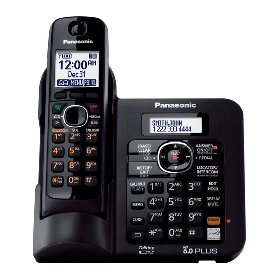
Caller ID Compatible
KX-TGA660B
(Handset)
(Charger Unit)
Configuration for each model
Model No
Base Unit
Handset
KX-TG6641 1 (TG6641) 1 (TGA660)
KX-TG6643 1 (TG6641) 3 (TGA660)
KX-TG6644 1 (TG6641) 4 (TGA660)
KX-TG6645 1 (TG6641) 5 (TGA660)
KX-TGA660*
1 (TGA660)
*KX-TGA660 is also an optional accessory, which contains a
handset and a charger.
Information for optional accessories
You can expand your phone system by registering optional
handsets (KX-TGA410 / KX-TGA659) to a single base unit.
Optional handsets and the supplied handset are different model
so that some functions may not be available.
Refer to each Operating Instruction for details.
KX-TG6641B
(Base Unit)
Charger Unit Expandable
Up to 6
2
Up to 6
3
Up to 6
4
Up to 6
1
Telephone Equipment
KX-TG6641B
Model No.
KX-TG6643B
KX-TG6644B
KX-TG6645B
KX-TGA660B
Digital Cordless Answering System
B: Black Version
(for U.S.A.)
© Panasonic System Networks Co., Ltd. 2011
Unauthorized copying and distribution is a violation
of law.
ORDER NO. KM41102310CE
F13
Advertisement
Table of Contents

Related Manuals for Panasonic KX-TG6641B


Summary of Contents for Panasonic KX-TG6641B
- Page 1 Optional handsets and the supplied handset are different model so that some functions may not be available. Refer to each Operating Instruction for details. © Panasonic System Networks Co., Ltd. 2011 Unauthorized copying and distribution is a violation of law.
- Page 2 KX-TG6641B/KX-TG6643B/KX-TG6644B/KX-TG6645B/KX-TGA660B WARNING This service information is designed for experienced repair technicians only and is not designed for use by the general public. It does not contain warnings or cautions to advise non-technical individuals of potential dangers in attempting to service a product. Products powered by electricity should be serviced or repaired only by experienced professional technicians.
-
Page 3: Table Of Contents
KX-TG6641B/KX-TG6643B/KX-TG6644B/KX-TG6645B/KX-TGA660B TABLE OF CONTENTS PAGE PAGE 1 Safety Precautions----------------------------------------------- 4 15.4. Circuit Board (Handset_Main) ------------------------ 83 1.1. For Service Technicians --------------------------------- 4 15.5. Circuit Board (Handset_LED) ------------------------- 85 2 Warning -------------------------------------------------------------- 4 15.6. Circuit Board (Charger Unit)--------------------------- 86 2.1. Battery Caution--------------------------------------------- 4 16 Exploded View and Replacement Parts List ----------- 87 2.2. -
Page 4: Safety Precautions
KX-TG6641B/KX-TG6643B/KX-TG6644B/KX-TG6645B/KX-TGA660B 1 Safety Precautions 1.1. For Service Technicians • Repair service shall be provided in accordance with repair technology information such as service manual so as to prevent fires, injury or electric shock, which can be caused by improper repair work. -
Page 5: Discarding Of P. C. Board
KX-TG6641B/KX-TG6643B/KX-TG6644B/KX-TG6645B/KX-TGA660B 2.2.1. Suggested PbF Solder There are several types of PbF solder available commercially. While this product is manufactured using Tin, Silver, and Copper (Sn+Ag+Cu), you can also use Tin and Copper (Sn+Cu), or Tin, Zinc, and Bismuth (Sn+Zn+Bi). Please check the manufacturer's specific instructions for the melting points of their products and any precautions for using their product with other materials. -
Page 6: Specifications
KX-TG6641B/KX-TG6643B/KX-TG6644B/KX-TG6645B/KX-TGA660B 3 Specifications ■ ■ Standard: Bit rate: DECT 6.0 (Digital Enhanced Cordless 1,152 kbit/s ■ Telecommunications 6.0) Modulation: ■ Number of channels: GFSK (Gaussian Frequency Shift Keying) 60 Duplex Channels ■ RF transmission power: ■ Frequency range: 115 mW (max.) 1.92 GHz to 1.93 GHz... -
Page 7: Technical Descriptions
KX-TG6641B/KX-TG6643B/KX-TG6644B/KX-TG6645B/KX-TGA660B 4 Technical Descriptions 4.1. US-DECT Description The frequency range of 1.92 GHz-1.93 GHz is used. Transmitting and receiving carrier between base unit and handset is same frequency. Refer to Frequency Table (P.62). 4.1.1. TDD Frame Format 5 ms 5 ms Up Link ( Handset - >... - Page 8 KX-TG6641B/KX-TG6643B/KX-TG6644B/KX-TG6645B/KX-TGA660B 4.1.3. Signal Flowchart in the Radio Parts Reception Base unit: A voice signal from TEL line is encoded to digital data and converted into a 1.9GHz modulated radio signal by BBIC(IC501). The RF signal, after which is amplified in BBIC, is fed to selected antenna.
-
Page 9: Block Diagram (Base Unit_Main)
KX-TG6641B/KX-TG6643B/KX-TG6644B/KX-TG6645B/KX-TGA660B 4.2. Block Diagram (Base Unit_Main) -
Page 10: Block Diagram (Base Unit_Rf Part)
KX-TG6641B/KX-TG6643B/KX-TG6644B/KX-TG6645B/KX-TGA660B 4.3. Block Diagram (Base Unit_RF Part) ANT2 ANT2 ANT1 DA801 TXON RXON ANT1 KX-TG6641/6643/6644/6645 BLOCK DIAGRAM (Base Unit_RF Part) -
Page 11: Circuit Operation (Base Unit)
KX-TG6641B/KX-TG6643B/KX-TG6644B/KX-TG6645B/KX-TGA660B 4.4. Circuit Operation (Base Unit) General Description: (BBIC, Flash Memory, EERROM) is a digital speech/signal processing system that implements all the functions of speech compression, record and playback, and memory management required in a digital telephone answering machine. The BBIC system is fully controlled by a host processor. The host processor provides activation and control of all that functions as follows. - Page 12 KX-TG6641B/KX-TG6643B/KX-TG6644B/KX-TG6645B/KX-TGA660B 4.4.4. Power Supply Circuit/Reset Circuit The power supply voltage from AC adaptor is converted to VBAT (3.0V) in IC302. And +3.0V for peripherals and analog part is insulated from VBAT by Doubler of BBIC. Circuit Operation: +3.0V VBAT IC601...
- Page 13 KX-TG6641B/KX-TG6643B/KX-TG6644B/KX-TG6645B/KX-TGA660B 4.4.4.1. Charge Circuit The voltage from the AC adaptor is supplied to the charge circuits. +5.5V F301 CHARGE+ CHARGE-...
- Page 14 KX-TG6641B/KX-TG6643B/KX-TG6644B/KX-TG6645B/KX-TGA660B 4.4.5. Telephone Line Interface Telephone Line Interface Circuit: Function • Bell signal detection • ON/OFF hook and pulse dial circuit • Side tone circuit Bell signal detection and OFF HOOK circuit: In the idle mode, Q141 is open to cut the DC loop current and decrease the ring load. When ring voltage appears at the Tip (T) and Ring (R) leads (When the telephone rings), the AC ring voltage is transferred as follows: T →...
- Page 15 KX-TG6641B/KX-TG6643B/KX-TG6644B/KX-TG6645B/KX-TGA660B 4.4.6. Parallel Connection Detect Circuit/Auto Disconnect Circuit Function: In order to disable call waiting and stutter tone functions when using telephones connected in parallel, it is necessary to have a circuit that judges whether a telephone connected in parallel is in use or not. This circuit determines whether the telephone connected in parallel is on hook or off hook by detecting changes in the T/R voltage.
- Page 16 KX-TG6641B/KX-TG6643B/KX-TG6644B/KX-TG6645B/KX-TGA660B 4.4.7. Calling Line Identification (Caller ID)/Call Waiting Caller ID Function: Caller ID The caller ID is a chargeable ID which the user of a telephone circuit obtains by entering a contract with the telephone company to utilize a caller ID service. For this reason, the operation of this circuit assumes that a caller ID service contract has been entered for the circuit being used.
- Page 17 KX-TG6641B/KX-TG6643B/KX-TG6644B/KX-TG6645B/KX-TGA660B Call Waiting Caller ID Calling Identity Delivery on Call Waiting (CIDCW) is a CLASS service that allows a customer, while off-hook on an existing call, to receive information about a calling party on a waited call. The transmission of the calling information takes place almost immediately after the customer is alerted to the new call so he/she can use this information to decide whether to take the new call.
-
Page 18: Block Diagram (Handset)
KX-TG6641B/KX-TG6643B/KX-TG6644B/KX-TG6645B/KX-TGA660B 4.5. Block Diagram (Handset) VBAT ANT1 EEPROM 13.824 MHz VBAT CHG_DET RF part CHG_CTL RXON RSTN RESET TXON CHARGE Battery_ON VBAT BATTERY BBIC Receiver HSSPOUTP Headset Jack LOUT HSMIP 4.0V CN431 VBAT CHARGE HEADSET_DET (KEY) CP_OFF PUMP (BELL) KEY_LED... -
Page 19: Block Diagram (Handset_Rf Part)
KX-TG6641B/KX-TG6643B/KX-TG6644B/KX-TG6645B/KX-TGA660B 4.6. Block Diagram (Handset_RF Part) TXON DA801 RXON KX-TGA660 BLOCK DIAGRAM (Handset_RF Part) -
Page 20: Circuit Operation (Handset)
KX-TG6641B/KX-TG6643B/KX-TG6644B/KX-TG6645B/KX-TGA660B 4.7. Circuit Operation (Handset) 4.7.1. Outline Handset consists of the following ICs as shown in Block Diagram (Handset) (P.18). • DECT BBIC (Base Band IC): IC1 - All data signals (forming/analyzing ACK or CMD signal) - All interfaces (ex: Key, Detector Circuit, Charge, EEPROM, LCD) •... - Page 21 KX-TG6641B/KX-TG6643B/KX-TG6644B/KX-TG6645B/KX-TGA660B 4.7.3. Charge Circuit Circuit Operation: When charging the handset on the Base Unit, the charge current is as follows; DC+(6.5 V) → F301 → R371 → R372 →CHARGE+(Base) → CHARGE+(Handset) → Q4 → D7→ F1 → BATTERY+... Battery... BATTERY- → R45 → GND → CHARGE-(Handset)→ CHARGE-(Base) → GND → DC-(GND) In this way, the BBIC on Handset detects the fact that the battery is charged.
-
Page 22: Behavior Of Electric Power Failure
KX-TG6641B/KX-TG6643B/KX-TG6644B/KX-TG6645B/KX-TGA660B 4.8. Behavior of Electric Power Failure In case that the power from AC adaptor is lost and lose radio waves, BBIC (IC1) turns IC6 ON since handset presumes that base unit's power is failed. Base unit detects that power voltage of AC adaptor +5.5V is OFF at IC351, then turns Q351 ON. -
Page 23: Signal Route
KX-TG6641B/KX-TG6643B/KX-TG6644B/KX-TG6645B/KX-TGA660B 4.10. Signal Route SIGNAL ROUTE ROUTE HANDSET TX HANDSET MIC - R73/74 - C11/13 - RA4 - IC1(22/23) - <HANDSET_RF_TX_ROUTE> - ANT. --- ---ANT. - <BASE_UNIT_RF_RX_ROUTE> - IC501(46/47 - 28) - R181 - C184 - Q161 - Q141 - D101 - L101/[L102 - P101] - T/R(TEL LINE) - Page 24 KX-TG6641B/KX-TG6643B/KX-TG6644B/KX-TG6645B/KX-TGA660B RF part signal route SIGNAL ROUTE ROUTE HANDSET RF IC1(44/45) - L809 - C812 - DA801 - C895 - ANT [ TX_ROUTE ] HANDSET RF ANT - C895 - DA801 - C826 - IC1(46/47) [ RX_ROUTE ] IC501(44/45) - C812 - L809 - DA801 - C895 - DA802 - C894/C893 - ANT1/ANT2...
-
Page 25: Location Of Controls And Components
KX-TG6641B/KX-TG6643B/KX-TG6644B/KX-TG6645B/KX-TGA660B 5 Location of Controls and Components Refer to the Operating Instructions. Note: You can download and refer to the Operating Instructions (Instruction book) on TSN Server. 6 Installation Instructions Refer to the Operating Instructions. Note: You can download and refer to the Operating Instructions (Instruction book) on TSN Server. -
Page 26: Test Mode
KX-TG6641B/KX-TG6643B/KX-TG6644B/KX-TG6645B/KX-TGA660B 8 Test Mode 8.1. Engineering Mode 8.1.1. Base Unit Important: Make sure the address on LCD is correct when entering new data. Otherwise, you may ruin the unit. Soft keys {OFF} {OFF} Naviga tor key/ (Volume) key {FLASH} {FLASH}... - Page 27 KX-TG6641B/KX-TG6643B/KX-TG6644B/KX-TG6645B/KX-TGA660B Frequently Used Items (Base Unit) ex.) Items Address Default Data New Data Remarks Frequency 00 07 / 00 08 00/01 Use these items in a READ-ONLY mode to confirm the contents. Careless rewriting may 00 02 ~ 00 06 Given value cause serious damage to the computer system.
- Page 28 KX-TG6641B/KX-TG6643B/KX-TG6644B/KX-TG6645B/KX-TGA660B 8.1.2. Handset Important: Make sure the address on LCD is correct when entering new data. Otherwise, you may ruin the unit. Soft keys {OFF} {OFF} Naviga tor key/ (Volume) key {FLASH} {FLASH} {CALL WAIT} {CALL WAIT} Dial keypad Dial keypad...
- Page 29 KX-TG6641B/KX-TG6643B/KX-TG6644B/KX-TG6645B/KX-TGA660B Frequently Used Items (Handset) ex.) Items Address Default Data New Data Possible Adjusted Possible Adjusted Remarks Value MAX (hex) Value MIN (hex) Battery Low 00 12/00 13 00 / 00 (*2) Frequency 00 07 / 00 08 00 / 01...
-
Page 30: Service Mode
KX-TG6641B/KX-TG6643B/KX-TG6644B/KX-TG6645B/KX-TGA660B 9 Service Mode 9.1. How to Clear User Setting (Handset Only) Handset Press simultaneously until a beep sound is heard. Then single handset is initialized. (The contents of user setting are reset to factory default) *Usage time is not cleared. -
Page 31: Troubleshooting Guide
KX-TG6641B/KX-TG6643B/KX-TG6644B/KX-TG6645B/KX-TGA660B 10 Troubleshooting Guide 10.1. Troubleshooting Flowchart FLOW CHART Not working Power ON Base Unit Check Power Not playback Playback Pre-Message Check Playback Not record (*1) Record Check Record Link No link No charge Battery Charge Check Battery Charge Check Link... - Page 32 KX-TG6641B/KX-TG6643B/KX-TG6644B/KX-TG6645B/KX-TGA660B 10.1.1. Check Power 10.1.1.1. Base Unit Is the AC Adaptor inserted into AC outlet? (*1) AC Adaptor. Is output voltage of AC adaptor 5.5 V? Check Check Power Supply Circuit. Check VDDC (1.2 V): Test Point [VDDC] RSTN: Reset = "High"? Check Reset Circuit.
- Page 33 KX-TG6641B/KX-TG6643B/KX-TG6644B/KX-TG6645B/KX-TGA660B 10.1.2. Check Record 10.1.2.1. Base Unit Not record Incoming Message Check Telephone Line Interface Check Bell signal. [Bell]. Check Telephone Line Interface Does the unit catch line? [OFF HOOK]. Check Line In: Pin 16 of BBIC. Check ICM Recording in Signal Route.
- Page 34 KX-TG6641B/KX-TG6643B/KX-TG6644B/KX-TG6645B/KX-TGA660B <How to change the Auto Disconnect activation time and VOX level> A) Auto Disconnect activation time: Some Telephone Company lines (fiber or cable) ON Hook and OFF Hook voltages are lower than conventional lines, which may cause a malfunction of Auto Disconnect detection. To solve this problem, try changing the Auto Disconnect activation through the procedures below.
- Page 35 KX-TG6641B/KX-TG6643B/KX-TG6644B/KX-TG6645B/KX-TGA660B B) Vox level: It makes easier to detect a small voice (caller) by raising the sensitivity of VOX level. Therefore, the recording of TAM is not turned off during a detection. 1) ~ 2) are same as (A). 3) Press "5","1","1".
- Page 36 KX-TG6641B/KX-TG6643B/KX-TG6644B/KX-TG6645B/KX-TGA660B 10.1.3. Check Playback 10.1.3.1. Base Unit Check VDDC (1.2 V): Test Point [VDDC] Check Power Supply Circuit. Check output of BBIC (Pin 29, 31). Check BBIC and Flash Memory. Check Speaker and its surroundings. Cross Reference: Note: Power Supply Circuit/Reset Circuit (P.12) Flash Memory is IC601.
- Page 37 KX-TG6641B/KX-TG6643B/KX-TG6644B/KX-TG6645B/KX-TGA660B 10.1.5. Check Link 10.1.5.1. Base Unit Does Base Unit make link with normal working Base Unit is OK. Check Handset. Handset? Is the voltage of VBAT about 3.0 V? Check around Power Supply Circuit. Is the voltage of VDDC about 1.2 V? Adjust +3.0V voltage to 3.0 V.
- Page 38 KX-TG6641B/KX-TG6643B/KX-TG6644B/KX-TG6645B/KX-TGA660B 10.1.5.2. Handset Does Handset make link with Base Unit? Handset is OK. Check Base Unit. (Correct working unit) Is the voltage of TP VBAT about 2.2~2.8 V? Check the batteries. Check around Power Supply Circuit/Reset Circuit. Is the voltage of TP VDDC about 1.2 V? Is the voltage of TP 3.0 V about 3.0 V?
- Page 39 KX-TG6641B/KX-TG6643B/KX-TG6644B/KX-TG6645B/KX-TGA660B 10.1.6. Check the RF part 10.1.6.1. Finding out the Defective part 1. Prepare Regular HS(*1) and Regular BU(*2). 2. a. Re-register regular HS (Normal mode) to base unit (to be checked). If this operation fails in some ways, the base unit is defective.
- Page 40 KX-TG6641B/KX-TG6643B/KX-TG6644B/KX-TG6645B/KX-TGA660B 10.1.6.2. RF Check Flowchart Each item (1 ~ 5) of RF Check Flowchart corresponds to Check Table for RF part (P.41). Please refer to the each item. Start Link Control Check BBIC interface parts. confirmation signal (RF Block <->BBIC on BU/HS P.C.B)
- Page 41 KX-TG6641B/KX-TG6643B/KX-TG6644B/KX-TG6645B/KX-TGA660B 10.1.6.3. Check Table for RF part Item BU (Base Unit) Check HS (Handset) Check Link Confirmation Normal 1. Register Regular HS to BU (to be 1. Register HS (to be checked) to Regular checked). HS, BU Mode [Normal Mode] 2.
- Page 42 KX-TG6641B/KX-TG6643B/KX-TG6644B/KX-TG6645B/KX-TGA660B 10.1.6.4. TEST RANGE Check Circuit block which range is defective can be found by the following check. Item BU (Base Unit) Check HS (Handset) Check Range Confirmation TX TEST 1. Register Regular HS to BU (to be checked). 1. Register HS (to be checked) to Regular BU.
- Page 43 KX-TG6641B/KX-TG6643B/KX-TG6644B/KX-TG6645B/KX-TGA660B 10.1.7. Registering a Handset to the Base Unit The supplied handset and base unit arepre-registered. If for some reason the handset is not registered to the baseunit, re-register the handset. 1 Handset: {MENU} i # 1 3 0 2 Base unit: Press and hold {LOCATOR} forabout 5 seconds until theregistration tone sounds.
- Page 44 KX-TG6641B/KX-TG6643B/KX-TG6644B/KX-TG6645B/KX-TGA660B 10.1.9. Check Handset Transmission Check MIC of handset. Check handset Tx in Signal Route. Cross Reference: Signal Route (P.23) 10.1.10. Check Handset Reception Check speaker of handset. Check handset Rx in Signal Route. Cross Reference: Signal Route (P.23) Note: When checking the RF part, Refer to Check the RF part (P.39).
-
Page 45: Disassembly And Assembly Instructions
KX-TG6641B/KX-TG6643B/KX-TG6644B/KX-TG6645B/KX-TGA660B 11 Disassembly and Assembly Instructions 11.1. Disassembly Instructions 11.1.1. Base Unit Remove the 5 screws to remove the cabinet cover. Remove the solders. Cabinet cover Solders Remove the screw and pararell wire to remove the main P.C. board. - Page 46 KX-TG6641B/KX-TG6643B/KX-TG6644B/KX-TG6645B/KX-TGA660B Remove the screw to remove the Jack holder. Remove the 4 screws and pararell wire to remove the operational P.C.B board.
- Page 47 KX-TG6641B/KX-TG6643B/KX-TG6644B/KX-TG6645B/KX-TGA660B 11.1.2. Handset 2 screws Remove the 2 screws. Insert a JIG (PQDJ10006Y) between the cabinet body Cabinet body and the cabinet cover, then pull it along the gap to open the cabinet. Cabinet cover Likewise, open the other side of the cabinet.
- Page 48 KX-TG6641B/KX-TG6643B/KX-TG6644B/KX-TG6645B/KX-TGA660B 11.1.3. Charger Unit 2 charge terminals...
-
Page 49: How To Attach The Antenna
KX-TG6641B/KX-TG6643B/KX-TG6644B/KX-TG6645B/KX-TGA660B 11.2. How to Attach the Antenna Locate as the following figure... -
Page 50: How To Replace The Base Unit Lcd
KX-TG6641B/KX-TG6643B/KX-TG6644B/KX-TG6645B/KX-TGA660B 11.3. How to Replace the Base Unit LCD Fit the heatseal of a new LCD. Vertical Interval Tolerance 0.2mm Horizontal Interval Tolerance 0.2mm If interval tolerance between center lines is less than 0.2 mm, it is o.k. New LCD Operational P.C.B. - Page 51 KX-TG6641B/KX-TG6643B/KX-TG6644B/KX-TG6645B/KX-TGA660B Attach the LCD and fix by hook A (two points). Solder the wires.
-
Page 52: How To Replace The Handset Lcd
KX-TG6641B/KX-TG6643B/KX-TG6644B/KX-TG6645B/KX-TGA660B 11.4. How to Replace the Handset LCD Note: The illustrations are simplified in this page. They may differ from the actual product. P. C. board Vertical Interval Tolerance Peel off the FFC (Flexible Flat Cable) from 0.2 mm the LCD, in the direction of the arrow. Take care to ensure that the foil on the P.C. -
Page 53: Measurements And Adjustments
KX-TG6641B/KX-TG6643B/KX-TG6644B/KX-TG6645B/KX-TGA660B 12 Measurements and Adjustments This chapter explains the measuring equipment, the JIG connection, and the PC setting method necessary for the measurement in Troubleshooting Guide (P.31) 12.1. Equipment Required • Digital multi-meter (DMM): it must be able to measure voltage and current. - Page 54 KX-TG6641B/KX-TG6643B/KX-TG6644B/KX-TG6645B/KX-TGA660B 12.2.2. Connections (Handset) Connect the DC Power or Battery to BATT+ and BATT-. Connect the JIG cable GND (black) to GND. Connect the JIG cable UTX (yellow) to UTX and URX (red) to URX. URX (red) To Serial Port...
- Page 55 KX-TG6641B/KX-TG6643B/KX-TG6644B/KX-TG6645B/KX-TGA660B 12.2.3. How to install Batch file into P.C. Insert the Batch file CD-ROM into CD-ROM drive and copy PNZZTG**** folder to your PC (example: D drive). <Example for Windows> On your computer, click [Start], select Programs Open an MS-DOS mode window.
- Page 56 KX-TG6641B/KX-TG6643B/KX-TG6644B/KX-TG6645B/KX-TGA660B 12.2.4. Commands (Base Unit) See the table below for frequently used commands. Command name Function Example rdeeprom Read the data of EEPROM Type “rdeeprom 00 00 FF”, and the data from address “00 00” to “FF” is read out.
-
Page 57: Adjustment Standard (Base Unit)
KX-TG6641B/KX-TG6643B/KX-TG6644B/KX-TG6645B/KX-TGA660B 12.3. Adjustment Standard (Base Unit) When connecting the simulator equipment for checking, please refer to below. 12.3.1. Bottom View Note: (*1) is referred to No.2 of Check Check Table for RF part (P.41) (*2) is referred to Power Supply Circuit/Reset Circuit (P.12) -
Page 58: Adjustment Standard (Charger Unit)
KX-TG6641B/KX-TG6643B/KX-TG6644B/KX-TG6645B/KX-TGA660B 12.4. Adjustment Standard (Charger Unit) When connecting the simulator equipment for checking, please refer to below. 12.4.1. Bottom View Digital Volt Meter /2 W 3.0A DC POWER DC 5.5 V... -
Page 59: Adjustment Standard (Handset)
KX-TG6641B/KX-TG6643B/KX-TG6644B/KX-TG6645B/KX-TGA660B 12.5. Adjustment Standard (Handset) When connecting the simulator equipment for checking, please refer to below. 12.5.1. Component View PNLB1885 KX-TGA660 RECEIVER C505 C896 C138 C859 C814 C812 C813 C822 C820 C810 R807 C805 C806 C188 CHG_CTRL VBAT_MON C65 C64... -
Page 60: Things To Do After Replacing Ic Or X'tal
KX-TG6641B/KX-TG6643B/KX-TG6644B/KX-TG6645B/KX-TGA660B 12.6. Things to Do after Replacing IC or X'tal If repairing or replacing EEPROM and X'tal, it is necessary to download the required data such as Programming data or adjustment data, etc in memory. The set doesn't operate if it is not executed. - Page 61 KX-TG6641B/KX-TG6643B/KX-TG6644B/KX-TG6645B/KX-TGA660B 12.6.1.2. Handset First, operate the PC setting according to The Setting Method of JIG (P.53). Then download the appropriate data according to the following procedures. Items How to download/Required adjustment EEPROM (IC3) Adjusted parameter data is stored in memory.
-
Page 62: Frequency Table
KX-TG6641B/KX-TG6643B/KX-TG6644B/KX-TG6645B/KX-TGA660B 12.7. Frequency Table Ch. (hex) TX/RX Frequency (MHz) Channel 0 1928.448 Channel 1 1926.720 Channel 2 1924.992 Channel 3 1923.264 Channel 4 1921.536... -
Page 63: Miscellaneous
KX-TG6641B/KX-TG6643B/KX-TG6644B/KX-TG6645B/KX-TGA660B 13 Miscellaneous 13.1. How to Replace the LLP (Leadless Leadframe Package) IC Note: This description is only applied on the model with Shield case. 13.1.1. Preparation • PbF (: Pb free) Solder • Soldering Iron Tip Temperature of 700 °F ± 20 °F (370 °C ± 10 °C) Note: We recommend a 30 to 40 Watt soldering iron. - Page 64 KX-TG6641B/KX-TG6643B/KX-TG6644B/KX-TG6645B/KX-TGA660B 13.1.4. How to Install the IC 1. Place the solder a little on the land where the radiation GND pad on IC bottom is to be attached. Soldering Iron Land Solder P.C.Board 2. Place the solder a little on the land where IC pins are to be attached, then place the IC.
-
Page 65: How To Replace The Flat Package
KX-TG6641B/KX-TG6643B/KX-TG6644B/KX-TG6645B/KX-TGA660B 13.2. How to Replace the Flat Package IC Even if you do not have the special tools (for example, a spot heater) to remove the Flat IC, with some solder (large amount), a soldering iron and a cutter knife, you can easily remove the ICs that have more than 100 pins. - Page 66 KX-TG6641B/KX-TG6643B/KX-TG6644B/KX-TG6645B/KX-TGA660B 13.2.3. How to Install the IC 1. Temporarily fix the FLAT PACKAGE IC, soldering the two marked pins. *Check the accuracy of the IC setting with the corresponding soldering foil. 2. Apply flux to all pins of the FLAT PACKAGE IC.
-
Page 67: Terminal Guide Of The Ics, Transistors And Diodes
KX-TG6641B/KX-TG6643B/KX-TG6644B/KX-TG6645B/KX-TGA660B 13.3. Terminal Guide of the ICs, Transistors and Diodes 13.3.1. Base Unit (Reverse View) C0CBCCC00103 PNWI1TG6641H C0EBE0000124 B1GFCFEN0011 C0CBAYG00016 C2HBCY000080 PNWI2TG6631H B1ABCF000103, B1ABDM000001 B1ADNB000003, B1GBCFYY0020 B1ACGP000008 DSC7003S0L PQVDMD5S 2SA1576S, B1GBCFYY0010 Cathode Cathode Cathode Anode Cathode Anode Anode Anode 1SS355... -
Page 68: Schematic Diagram
KX-TG6641B/KX-TG6643B/KX-TG6644B/KX-TG6645B/KX-TGA660B 14 Schematic Diagram 14.1. For Schematic Diagram 14.1.1. Base Unit (Schematic Diagram (Base Unit_Main)) Notes: 1. DC voltage measurements are taken with voltmeter from the negative voltage line. Important Safety Notice: Components identified by mark have special characteristics important for safety. - Page 69 KX-TG6641B/KX-TG6643B/KX-TG6644B/KX-TG6645B/KX-TGA660B Memo...
-
Page 70: Schematic Diagram (Base Unit_Main)
KX-TG6641B/KX-TG6643B/KX-TG6644B/KX-TG6645B/KX-TGA660B 14.2. Schematic Diagram (Base Unit_Main) VCCA ANT1 R807 RXON C822 C827 C892 ANT1 W 0.2mm W 0.15mm 1st layer L 20mm 3rd layer C894 C826 C820 1.5p ANT2 DA801 C805 C895 L809 C812 2.7p 1.2p 7.5n 0.9p DA802 C893... - Page 71 KX-TG6641B/KX-TG6643B/KX-TG6644B/KX-TG6645B/KX-TGA660B +3.0V Q141 REFERENCE R160 1XX : TEL LINE 3XX : POWER, CHARGE 4XX : MIC, SP Q161 5XX : BBIC R141 6XX : FLASH, EEPROM, KEY, LCD 7XX : FOR DK/BT 100k 8XX : RF C165 NC C163 NC...
-
Page 72: Schematic Diagram (Base Unit_Operation)
KX-TG6641B/KX-TG6643B/KX-TG6644B/KX-TG6645B/KX-TGA660B 14.3. Schematic Diagram (Base Unit_Operation) CN901 LCD_Light OPT_PWR /CS1 /RES SCL (D6) SI (D7) LED902 VDDA MEG_LED LED901 ANS_LED C903 1u 16V LCD_GND 13pin:TG6641 LCD_RST R907 100 LCD_CS LCD_CD CELL1_2 CELL2_2 LCD_SID R908 100 CELL1_1 CELL2_1 BT_HS LCD_SCL LCD_VDD... -
Page 73: Schematic Diagram (Base Unit_Led)
KX-TG6641B/KX-TG6643B/KX-TG6644B/KX-TG6645B/KX-TGA660B 14.4. Schematic Diagram (Base Unit_LED) WLED NC: No Components KX-TG6641/6643/6644/6645 SCHEMATIC DIAGRAM (Base Unit_LED) -
Page 74: Schematic Diagram (Handset_Main)
KX-TG6641B/KX-TG6643B/KX-TG6644B/KX-TG6645B/KX-TGA660B 14.5. Schematic Diagram (Handset_Main) Charge Current VBAT VBAT BATT+ 2.5A CHG_CUR BATT- To Battery 3.0V When on Charge C172 0.1u 3.3k E_WP EEP_WP E_SCL EEP_SCL CONT Battery_ON E_SDA EEP_SDA VOUT * BBIC initialization stand-by status * When "SFR" command is executed, 13.824MHz... - Page 75 KX-TG6641B/KX-TG6643B/KX-TG6644B/KX-TG6645B/KX-TGA660B R807 RXON RF BLOCK W 0.15mm L 20mm W 0.15mm/L 7mm 3rd layer W 0.5mm /L 5mm C826 1st layer ANT-Short-GND RX_RF ANT-Short C895 1.3p G ND C812 L809 8.2n DA801 W 0.15mm TX_RF L 20mm 3rd layer W 0.2mm R806 L 10.0mm...
-
Page 76: Schematic Diagram (Handset_Led)
KX-TG6641B/KX-TG6643B/KX-TG6644B/KX-TG6645B/KX-TGA660B 14.6. Schematic Diagram (Handset_LED) KX-TGA660 SCHEMATIC DIAGRAM (Handset_LED) -
Page 77: Schematic Diagram (Charger Unit)
KX-TG6641B/KX-TG6643B/KX-TG6644B/KX-TG6645B/KX-TGA660B 14.7. Schematic Diagram (Charger Unit) 6.8 (2W) SCHEMATIC DIAGRAM (Charger Unit) - Page 78 KX-TG6641B/KX-TG6643B/KX-TG6644B/KX-TG6645B/KX-TGA660B Memo...
-
Page 79: Printed Circuit Board
KX-TG6641B/KX-TG6643B/KX-TG6644B/KX-TG6645B/KX-TGA660B 15 Printed Circuit Board 15.1. Circuit Board (Base Unit_Main) 15.1.1. Component View C894 C343 C890 C306 ANT2 R322 R321 P101 C382 C341 C381 PNLB1883Z C342 JOINT2 D101 SA101 IC381 X501 YL-W DA802 R891 R806 C508 R509 C509 MSG_LED KEYS_E... - Page 80 KX-TG6641B/KX-TG6643B/KX-TG6644B/KX-TG6645B/KX-TGA660B 15.1.2. Bottom View For JIG ANT1 ANT2 +5.5V UGND VBAT C301 VBAT 3.0A F301 R331 PNLB1883Z R332 C115 R115 C331 C121 C122 YL-W R111 R122 C112 VCCA C510 C114 C457 C514 C458 C511 C512 VREF L661 Q111 C530 R507...
-
Page 81: Circuit Board (Base Unit_Operation)
KX-TG6641B/KX-TG6643B/KX-TG6644B/KX-TG6645B/KX-TGA660B 15.2. Circuit Board (Base Unit_Operation) BL+ BL- CELL1_1 CELL1_2 R908 R907 BT_HS C903 C902 CELL2_1 CELL2_2 ERASE MSG1 MSG2 SKIP MSG3 MSG4 STOP LOCAT/INT DOWN FLASH HOLD MEMO MUTE CONF MIC+ MIC- PHONEBOOK KX-TG6641/6643/6644/6645 CIRCUIT BOARD (Base Unit_Operation (Component View)) -
Page 82: Circuit Board (Base Unit_Led)
KX-TG6641B/KX-TG6643B/KX-TG6644B/KX-TG6645B/KX-TGA660B 15.3. Circuit Board (Base Unit_LED) PNLB1921Z KX-TG6641/6643/6644/6645 CIRCUIT BOARD (Base Unit_LED (Component View)) -
Page 83: Circuit Board (Handset_Main)
KX-TG6641B/KX-TG6643B/KX-TG6644B/KX-TG6645B/KX-TGA660B 15.4. Circuit Board (Handset_Main) 15.4.1. Component View PNLB1885 ANT-TP ANT-GND KX-TGA660 RECEIVER C505 C896 C138 C859 C814 C812 C813 C822 C820 C810 R807 C805 C806 C188 CKM/STM (CLK:13.824MHz) CHG_CTRL VBAT_MON C65 C64 C96 C86 VBG/CHG_MON 3.0V (output) C172 4.0V... - Page 84 KX-TG6641B/KX-TG6643B/KX-TG6644B/KX-TG6645B/KX-TGA660B 15.4.2. Bottom View LED12 CN3_C SOFT1 MENU SOFT2 TALK LED2 LED5 LEFT RIGHT FLASH DOWN KX-TGA660 CIRCUIT BOARD (Handset_Main (Bottom View))
-
Page 85: Circuit Board (Handset_Led)
KX-TG6641B/KX-TG6643B/KX-TG6644B/KX-TG6645B/KX-TGA660B 15.5. Circuit Board (Handset_LED) PNLB1964Z KX-TGA660 CIRCUIT BOARD (Handset_LED (Component View)) -
Page 86: Circuit Board (Charger Unit)
KX-TG6641B/KX-TG6643B/KX-TG6644B/KX-TG6645B/KX-TGA660B 15.6. Circuit Board (Charger Unit) 15.6.1. Component View CIRCUIT BOARD (Charger Unit (Component View)) 15.6.2. Bottom View 3.0A CIRCUIT BOARD (Charger Unit (Bottom View)) -
Page 87: Exploded View And Replacement Parts List
KX-TG6641B/KX-TG6643B/KX-TG6644B/KX-TG6645B/KX-TGA660B 16 Exploded View and Replacement Parts List 16.1. Cabinet and Electrical Parts (Base Unit) (*1) PCB3 PCB1 PCB2 MIC1 Ref.No. Figure 2.6 x 8mm Note: (*1) This cable is fixed by welding. Refer to How to Replace the Base Unit LCD (P.50). -
Page 88: Cabinet And Electrical Parts (Handset)
(*1) This cable is fixed by welding. Refer to How to Replace the Handset LCD (P.52). (*2) The rechargeable Ni-MH battery HHR-4DPA is available through sales route of Panasonic. (*3) Attach the SPACER (No. 121) to the exact location described above. -
Page 89: Cabinet And Electrical Parts (Charger Unit)
KX-TG6641B/KX-TG6643B/KX-TG6644B/KX-TG6645B/KX-TGA660B 16.3. Cabinet and Electrical Parts (Charger Unit) 200-1 PCB200 200-2 200-3 200-4 Ref.No. Figure 2×8 mm φ... -
Page 90: Accessories And Packing Materials
KX-TG6641B/KX-TG6643B/KX-TG6644B/KX-TG6645B/KX-TGA660B 16.4. Accessories and Packing Materials 16.4.1. KX-TG6641B (*1) (*1) Note: (*1)These pads are pieces of Ref No.P1 (GIFT BOX). - Page 91 KX-TG6641B/KX-TG6643B/KX-TG6644B/KX-TG6645B/KX-TGA660B 16.4.2. KX-TG6643B A104 A103 A102 P102 P102 A101 (*1) P102 P101 Note: (*1) This pad is a piece of Ref No.P101 (GIFT BOX).
- Page 92 KX-TG6641B/KX-TG6643B/KX-TG6644B/KX-TG6645B/KX-TGA660B 16.4.3. KX-TG6644B A204 A203 P202 A202 P202 A201 P202 (*1) P201 Note: (*1) This pad is a piece of Ref No.P201 (GIFT BOX).
- Page 93 KX-TG6641B/KX-TG6643B/KX-TG6644B/KX-TG6645B/KX-TGA660B 16.4.4. KX-TG6645B P302 A304 (*1) A301 (*1) A302 P302 A303 A301 (*1) (*1) P301 Note: (*1)These pads are pieces of Ref No.P301 (GIFT BOX).
- Page 94 KX-TG6641B/KX-TG6643B/KX-TG6644B/KX-TG6645B/KX-TGA660B 16.4.5. KX-TGA660B A403 A402 (*1) A401 P401 Note: (*1)This pad is a piece of Ref No.P401 (GIFT BOX).
-
Page 95: Replacement Parts List
KX-TG6641B/KX-TG6643B/KX-TG6644B/KX-TG6645B/KX-TGA660B 16.5. Replacement Parts List Safety Ref. Part No. Part Name & Description Remarks 1. RTL (Retention Time Limited) PNHR1381Z GUIDE, BUTTON PS-HB Note: PNBC1345Z1 BUTTON, MESSAGE PS-HB The “RTL” marking indicates that its Retention Time is PNJK1101Z KEYBOARD SWITCH, TAM... - Page 96 KX-TG6641B/KX-TG6643B/KX-TG6644B/KX-TG6645B/KX-TGA660B Safety Ref. Part No. Part Name & Description Remarks Safety Ref. Part No. Part Name & Description Remarks RA652 EXB28V101JX RESISTOR ARRAY C111 F1J2A473A024 0.047 (VARISTOR) C112 F1J2A473A024 0.047 SA101 J0LF00000048 VARISTOR (SURGE C113 PQCUV1A684KB 0.68 ABSORBER) C120 ECUE1H102KBQ 0.001...
- Page 97 KX-TG6641B/KX-TG6643B/KX-TG6644B/KX-TG6645B/KX-TGA660B Safety Ref. Part No. Part Name & Description Remarks Safety Ref. Part No. Part Name & Description Remarks C812 F1G1HR90A480 0.9p L0AA02A00095 SPEAKER C813 F1G1H2R0A480 2p PQHS10784Y SPACER, SPEAKER NET C820 F1G1H1R5A480 1.5p PQJC10056W BATTERY TERMINAL C822 ECUE1H100DCQ 10p...
- Page 98 KX-TG6641B/KX-TG6643B/KX-TG6644B/KX-TG6645B/KX-TGA660B Safety Ref. Part No. Part Name & Description Remarks Safety Ref. Part No. Part Name & Description Remarks ERJ2GEJ103 ECUE1A104KBQ 0.1 ERJ2GEJ104 100k ECUE1A104KBQ 0.1 ERJ8GEYJ3R3 ECJ1VB0G106M 10 ERJ2GEJ303 ECUV1A105KBV 1 ERJ2RKF2003 200k ECUV1A105KBV 1 ERJ2RKF1003 100k ECUE0J105KBQ 1...
- Page 99 (*1) See Equipment Required (P.53), and The Setting (*1) You can download and refer to the Operating Method of JIG (P.53) Instructions (Instruction book) on TSN Server. (*2) When replacing the Handset LCD, See How to 16.5.4.1. KX-TG6641B Replace the Handset LCD (P.52) Safety Ref. Part No.