Table of Contents
Advertisement
Quick Links
Notes: Please use this manual together with service manual
Model No.(SA-MAX8000GN), Order no. (PSG1502011CE).
• CD Mechanism Unit, Order No. PSG1303059AE
• Speaker system SB-MAX8000GS, Order No: PSG1503012AE
TABLE OF CONTENTS
1 Notes ----------------------------------------------------------------- 3
2 Safety Precautions----------------------------------------------- 4
2.1. General Guidelines---------------------------------------- 4
2.2. Before Repair and Adjustment ------------------------- 4
2.3. Protection Circuitry ---------------------------------------- 5
2.4. Caution For Fuse Replacement------------------------ 5
2.5. Safety Parts Information -------------------------------- 5
3 Warning -------------------------------------------------------------- 6
Model No.
Product Color: (K)...Black Type
PAGE
to Electrostatically Sensitive (ES) Devices ----------6
3.2. Precaution of Laser Diode -------------------------------6
(PbF) ---------------------------------------------------------- 7
3.4. Handling Precautions for Traverse Ass'y ------------7
prevention----------------------------------------------------8
4 Specifications ------------------------------------------------------9
© Panasonic Corporation 2015. All rights reserved.
Unauthorized copying and distribution is a violation of
law.
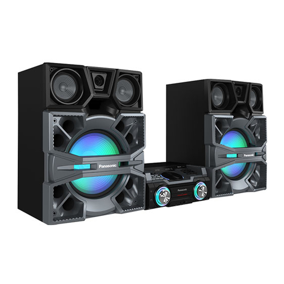
CD Stereo System
SA-MAX8000GM
SA-MAX8000GS
PSG1505002AE
PAGE
Advertisement
Table of Contents

Related Manuals for Panasonic SA-MAX8000GM


Summary of Contents for Panasonic SA-MAX8000GM
-
Page 1: Table Of Contents
3.4. Handling Precautions for Traverse Ass’y ------------7 2.5. Safety Parts Information -------------------------------- 5 3.5. Grounding electrostatic breakdown 3 Warning -------------------------------------------------------------- 6 prevention----------------------------------------------------8 4 Specifications ------------------------------------------------------9 © Panasonic Corporation 2015. All rights reserved. Unauthorized copying and distribution is a violation of law. - Page 2 5 Block Diagram --------------------------------------------------- 11 5.1. System Control ------------------------------------------- 11 5.2. Audio -------------------------------------------------------- 15 5.3. Power Supply --------------------------------------------- 17 6 Schematic Diagram--------------------------------------------- 19 6.1. Main (IO Expansion) Circuit --------------------------- 19 6.2. Main (Fan LED) Circuit --------------------------------- 20 6.3. Main (DSP) Circuit --------------------------------------- 21 6.4.
-
Page 3: Notes
1 Notes This service manual contains technical information which will allow service personnel’s to understand and service this model. Please place orders using the parts list and not the drawing reference numbers. If the circuit is changed or modified, this information will be followed by supplement service manual to be filed with original service manual. -
Page 4: Safety Precautions
2 Safety Precautions 2.1. General Guidelines 1. IMPORTANT SAFETY NOTICE There are special components used in this equipment which are important for safety. These parts are marked by in the Schematic Diagrams, Circuit Board Layout, Exploded Views and Replacement Parts List. It is essential that these critical parts should be replaced with manufacturer’s specified parts to prevent X-RADIATION, shock, fire, or other hazards. -
Page 5: Protection Circuitry
2.3. Protection Circuitry The protection circuitry may have operated if either of the following conditions are noticed: • No sound is heard when the power is turned on. • Sound stops during a performance. The function of this circuitry is to prevent circuitry damage if, for example, the positive and negative speaker connection wires are “shorted”, or if speaker systems with an impedance less than the indicated rated impedance of the amplifier are used. -
Page 6: Warning
3 Warning 3.1. Prevention of Electrostatic Discharge (ESD) to Electrostatically Sensi- tive (ES) Devices Some semiconductor (solid state) devices can be damaged easily by static electricity. Such components commonly are called Elec- trostatically Sensitive (ES) Devices. The following techniques should be used to help reduce the incidence of component damage caused by electrostatic discharge (ESD). -
Page 7: General Description About Lead Free Solder (Pbf)
Figure 2-1 3.3. General description about Lead Free Solder (PbF) The lead free solder has been used in the mounting process of all electrical components on the printed circuit boards used for this equipment in considering the globally environmental conservation. The normal solder is the alloy of tin (Sn) and lead (Pb). -
Page 8: Grounding For Electrostatic Breakdown Prevention
ble cable, cut off the antistatic FFC. Figure 2-2 3.5. Grounding for electrostatic breakdown prevention • As for parts that use optical pick-up (laser diode), the optical pick-up is destroyed by the static electricity of the working environ- ment. Repair in the working environment that is grounded. 3.5.1. -
Page 9: Specifications
*MPEG-1 Layer 3, MPEG-2 Layer 3 2. Total harmonic distortion is measured by the digital spec- Pick up trum analyzer. Wavelength 790 nm(CD) System: SC-MAX8000GM ® Main Unit: SA-MAX8000GM Buetooth section Speaker System: SB-MAX8000GS Version ® Bluetooth 2.1 + EDR... -
Page 11: Block Diagram
5 Block Diagram 5.1. System Control : USB SIGNAL LINE : CD SIGNAL LINE : TUNER/AUX SIGNAL LINE MAIN P.C.B. CD MECHANISM UNIT OPTICAL IC1001 PICKUP UNIT BUTTON LEFT P.C.B. P5002 P5002 P5002 CD TRACKING SIGNAL P5002 P1802 P1500 P1502 P1600 DJ JOG A DJ JOG A... - Page 12 : CD SIGNAL LINE : TUNER/AUX SIGNAL LINE : USB SIGNAL LINE MAIN P.C.B. BUTTON LEFT P.C.B. MULTI CONTROL P.C.B. IC1001 BUTTON RIGHT P.C.B. S1500 S1650 S1656 S1657 S1659 POWER OPEN/CLOSE STOP/TUNE MODE BT -PAIRING MEMORY/USB P1802 P1500 P1502 P1600 P1602 P1650 KEY A...
- Page 13 : CD SIGNAL LINE : TUNER/AUX SIGNAL LINE : USB SIGNAL LINE MAIN P.C.B. SPEAKERS SB-MAX8000 P1502 ILLUMINATION JOG P.C.B. ILLUMINATION RIGHT P.C.B. P1502 TO SYSTEM CONTROL TO SYSTEM CONTROL P1502 P1930 P1960 P1961 P1980 BLOCK (4/4) BLOCK (2/4) P1502 P1930 P1960 P1961...
- Page 14 : CD SIGNAL LINE : TUNER/AUX SIGNAL LINE : USB SIGNAL LINE MAIN P.C.B. TO SYSTEM CONTROL DC DET BLOCK (3/4) DC DET FROM AUDIO IC1001 IC1004 EEPROM SCL1 6 SCL IC8501 SDA1 5 SDA FAN CONTROL LRCKI1 Q8501,Q8502,Q8503 TUN WCK TUN WCK LRCKO1 Q8504,Q8505...
-
Page 15: Audio
5.2. Audio : CD SIGNAL LINE : TUNER/AUX/MIC SIGNAL LINE : AUDIO SIGNAL LINE : AM SIGNAL LINE : FM SIGNAL LINE IC4005 MAIN P.C.B. 6 SDIN3 MIC DET2 CN1401 P1803 MIC DET2 MIC DET2 TO SYSTEM CONTROL CN1401 P1803 MIC DET1 MIC DET1 JK1403... - Page 16 : CD SIGNAL LINE : TUNER/AUX/MIC SIGNAL LINE : AUDIO SIGNAL LINE : AM SIGNAL LINE : FM SIGNAL LINE SPEAKERS MAIN P.C.B. Q4505 AMPLIFIER JK4201 38 IN3 LEFT LOW JK4201 46 IN1 40 IN4 Q4506 AMPLIFIER 44 IN2 Q4502 AMPLIFIER Q4509 DC DET...
-
Page 17: Power Supply
5.3. Power Supply MAIN P.C.B. SMPS P.C.B. IC1402 IC8001 +1.5V VOLTAGE SWITCHING MODE POWER SUPPLY CONTROL REGULATOR T1401 PW SYS3R3V PW SOC 1R5V PW SOC 1R5V +1.5V TRANSFORMER 4 VIN VO 3 CL 3 D1404 PW XSW3R3V +3.3V 1 CN VCC 4 D1601 CN1851... - Page 18 MAIN P.C.B. BUTTON LEFT P.C.B. BT&NFC P.C.B. PW BT SW4R6V BT 4R6V P1802 P1500 P1504 P7701* BT 4R6V NFC D3R3V P1504 P7701* NFC D3R3V +3.3V +3.3V FL DISPLAY P.C.B. P1802 P1500 P1502 P1600 P1601 P1700 PW STBY3R3V PW STBY3R3V +3.3V +3.3V IC1002 VOLTAGE...
-
Page 19: Schematic Diagram
6 Schematic Diagram 6.1. Main (IO Expansion) Circuit SCHEMATIC DIAGRAM - 1 MAIN (IO EXPANSION) CIRCUIT : +B SIGNAL LINE : AUX/MIC SIGNAL LINE C1826 1000P R1805 P1802 J0JYC0000656 USBLED_REC REM_IN REM_IN USBLED_PLAY1 LB1201 PW_XSW3R3V PW_STBY3R3V R1236 YMH_INPUT_SEL J0JYC0000656 C1804 1000P DGND SP_INT... -
Page 20: Main (Fan Led) Circuit
6.2. Main (Fan LED) Circuit SCHEMATIC DIAGRAM - 2 MAIN (FAN LED) CIRCUIT : +B SIGNAL LINE IC1501 P1501 AN32183A-VF LED DRIVER LB1508 TO SB-MAX8000 J0JYC0000656 R1501 PW_SW3R3V IREF C1525 R1504 I2C_SCL AGND I2C_SDA NRST ILUMI_NRST R1503 SLAVSEL C1505 C1506 R1508 CLKIO KIRARI_IN... -
Page 21: Main (Dsp) Circuit
6.3. Main (DSP) Circuit SCHEMATIC DIAGRAM - 3 MAIN (DSP) CIRCUIT : +B SIGNAL LINE : -B SIGNAL LINE : CD SIGNAL LINE : TUNER/AUX/MIC SIGNAL LINE : AUDIO SIGNAL LINE C4055 R4037 FL+_HI 1.5K R4034 R4031 C4033 C4080 R4057 R4038 R4030 5.6K... -
Page 22: Main (Amp Btl) Circuit (1/2)
6.4. Main (Amp BTL) Circuit (1/2) SCHEMATIC DIAGRAM - 4 MAIN (AMP BTL) CIRCUIT : +B SIGNAL LINE : -B SIGNAL LINE : AUDIO SIGNAL LINE AMP_GND D4508 B0ACGM000002 R4549 R4516 R4519 5.6K 4.7K R4547 D4507 B0ACGM000002 R4548 R4552 C4528 C4584 R4550 3.9K... -
Page 23: Main (Amp Btl) Circuit (2/2)
6.5. Main (Amp BTL) Circuit (2/2) SCHEMATIC DIAGRAM - 5 MAIN (AMP BTL) CIRCUIT : +B SIGNAL LINE : -B SIGNAL LINE : AUDIO SIGNAL LINE L4506 G0C100M00013 P4501 PW_+40V +B (40V) C4599 +B (40V) AMP_GND +B (40V) C4555 C4567 C4560 50V3300 PWR_GND... -
Page 24: Main (Micon) Circuit (1/2)
6.6. Main (MICON) Circuit (1/2) SCHEMATIC DIAGRAM - 6 MAIN (MICON) CIRCUIT : +B SIGNAL LINE : -B SIGNAL LINE : CD SIGNAL LINE : TUNER/AUX/MIC SIGNAL LINE : USB SIGNAL LINE BT_UART_RTS BT_UART_RTS BT_UART_RX BT_UART_RX BT_UART_TX BT_UART_TX C2009 C2005 LB2001 J0JYC0000656 PW_SW3R3V... -
Page 25: Main (Micon) Circuit (2/2)
6.7. Main (MICON) Circuit (2/2) SCHEMATIC DIAGRAM - 7 MAIN (MICON) CIRCUIT : +B SIGNAL LINE : -B SIGNAL LINE : CD SIGNAL LINE : TUNER/AUX/MIC SIGNAL LINE : USB SIGNAL LINE IC1003 RFKWFX8000AM 16M FLASH MEMORY DSP_WCK DSP_BCK DSP_SDO0 LB1006 HOLD J0JYC0000656... -
Page 26: Main (Amp Single) Circuit (1/2)
6.8. Main (Amp Single) Circuit (1/2) SCHEMATIC DIAGRAM - 8 MAIN (AMP SINGLE) CIRCUIT : +B SIGNAL LINE : -B SIGNAL LINE : AUDIO SIGNAL LINE TO MAIN (AMP SINGLE) C4279 C4278 IC4201 R4282 CIRCUIT (2/2) C0JBAB000902 C4277 100P OSCILLATOR AMP R4281 X4201 R4293... -
Page 27: Main (Amp Single) Circuit (2/2)
6.9. Main (Amp Single) Circuit (2/2) SCHEMATIC DIAGRAM - 9 MAIN (AMP SINGLE) CIRCUIT : +B SIGNAL LINE : -B SIGNAL LINE : AUDIO SIGNAL LINE TO MAIN (AMP SINGLE) PW_+40V CIRCUIT (1/2) D4215 C4254 C4280 B0HCMM000024 50V3300 C4283 D4214 RL4201* GND_PW Q4206... -
Page 28: Main (Fe) Circuit
6.10. Main (FE) Circuit SCHEMATIC DIAGRAM - 10 MAIN (FE) CIRCUIT : +B SIGNAL LINE : CD SIGNAL LINE OPEN_SW INNER_SW CLOSE_SW C5009 LB5003 J0JHC0000045 PW_CD_SW5R4V C5010 0.01 LD_CCW C5031 C5030 C5029 C5028 C5027 LD_CW 100P 100P 100P 1000P 100P R5011 6.8K P5001... -
Page 29: Main (Karaoke) Circuit
6.11. Main (Karaoke) Circuit SCHEMATIC DIAGRAM - 11 MAIN (KARAOKE) CIRCUIT : +B SIGNAL LINE : CD SIGNAL LINE : TUNER/AUX/MIC SIGNAL LINE DGND IC4802 C0FBAY000032 R4820 A/D CONVERTER RX4802 R4823 D1H81034A042 SCLK LRCK R4822 SDTO R4821 MCLK RX4801 C4820 D1H81014A042 DGND C4819... -
Page 30: Main (Digital Power) Circuit (1/2)
6.12. Main (Digital Power) Circuit (1/2) SCHEMATIC DIAGRAM - 12 MAIN (DIGITAL POWER) CIRCUIT : +B SIGNAL LINE : -B SIGNAL LINE IC8011 C0DBEYY00267 +3.3V LDO R8068 GND GND PDET D8013 PW_SW15R0V B0JCGD000016 PW_SW5R4V VIN VOUT R8067 D8040 23.2K B0ADDH000009 L8005 G1C100KA0101 SYS5R0V... -
Page 31: Main (Digital Power) Circuit (2/2)
6.13. Main (Digital Power) Circuit (2/2) SCHEMATIC DIAGRAM - 13 MAIN (DIGITAL POWER) CIRCUIT : +B SIGNAL LINE : -B SIGNAL LINE IO: MAIN (IO EXPANSION): SCHEMATIC DIAGRAM - 1 FA: MAIN (FAN LED): SCHEMATIC DIAGRAM - 2 DS: MAIN (DSP): SCHEMATIC DIAGRAM - 3 AB: MAIN (AMP BTL): SCHEMATIC DIAGRAM - 4 ~ 5 MI: MAIN (MICON): SCHEMATIC DIAGRAM - 6 ~ 7 AS: MAIN (AMP SINGLE): SCHEMATIC DIAGRAM - 8 ~ 9... -
Page 32: Main (Usb) Circuit
6.14. Main (USB) Circuit SCHEMATIC DIAGRAM - 14 MAIN (USB) CIRCUIT : +B SIGNAL LINE : USB SIGNAL LINE USB_OE USB_SEL PW_XSW3R3V T9001 P9001 J0ZZB0000182 IC9001 DGND C0JBAS000401 D+ A USB SWITCH USB CIRCUIT D- A R9003 (CN9001) 2.2K DGND IN SCHEMATIC USB_D+ D+ B... -
Page 33: Main (Aux Tuner) Circuit
6.15. Main (AUX Tuner) Circuit SCHEMATIC DIAGRAM - 15 MAIN (AUX TUNER) CIRCUIT : +B SIGNAL LINE : TUNER/AUX SIGNAL LINE : AM SIGNAL LINE : FM SIGNAL LINE ANALOG_SEL LB4901 J0JYC0000656 PW_SW12R0V C4906 R4906 R4926 JK4951 QR4901 R4901 C4904 B1GBCFJJ0040 ANALOG_SEL2 SWITCH... -
Page 34: Button Left Circuit
6.16. Button Left Circuit SCHEMATIC DIAGRAM - 18 BUTTON LEFT CIRCUIT : +B SIGNAL LINE P1501 VOL_JOG_A VOL_JOG_A VOL_JOG_B VOL_JOG_B ILLUMI_JOG_A ILLUMI_JOG_A D1500 D1517 D1513 D1507 ILLUMI_JOG_B B3AAA0001129 DA2J10100L DA2J10100L DA2J10100L ILLUMI_JOG_B R1514 D1504 MAIN (IO EXPANSION) B3AAA0001129 CIRCUIT (P1801) IN SCHEMATIC P1504 DIAGRAM - 1... -
Page 35: Button Right And Multi Control Circuit
6.17. Button Right and Multi Control Circuit SCHEMATIC DIAGRAM - 19 BUTTON RIGHT CIRCUIT S1652 R1656 USB REC/PAUSE 3.9K S1651 R1655 MEMORY REC/PAUSE K1651 MAX8000GS/GM S1653 R1657 6.8K S1655 S1654 R1652 R1658 ALBUM/TRACK 7.5K 3.9K S1656 R1651 STOP/TUNE MODE 3.9K S1658 R1660 PLAY/PAUSE... -
Page 36: Mic Circuit
6.18. Mic Circuit SCHEMATIC DIAGRAM - 20 MIC CIRCUIT : +B SIGNAL LINE : AUX/MIC SIGNAL LINE C1431 4700P R1417 4.7K C1425 0.01 R1413 C1432 C1429 C1428 R1414 50V0.1 50V4.7 50V4.7 2.2K C1430 C1426 R1415 50V1 C1424 R1416 50V2.2 IC1400 C1AB00003130 MIC AMPLIFIER R1421... -
Page 37: Printed Circuit Board
7 Printed Circuit Board 7.1. Main P.C.B. (Side A) MAIN P.C.B. (RFKV5141EA) LB1802 C9005 R5009 LB1803 R5010 LB1804 C5012 LB5015 C5001 C9006 LB1807 LB1805 LB5014 LB1806 LB1808 C5002 C5004 IC5001 C5003 C2008 C2010 C5010 C5009 LB1005 R1034 C1023 R1032 R1031 R1026 C1006 R1033... -
Page 38: Main P.c.b. (Side B)
7.2. Main P.C.B. (Side B) MAIN P.C.B. (RFKV5141EA) P5002 LB5016 P1801 C5026 C5027 (TO OPTICAL C5025 PICKUP UNIT) P5001 P9002 C5023 C5018 R5023 C5031 C5028 C5015 C5029 C2009 Q5001 R9006 R9008 C5024 R5017 LB5010 R5015 C2012 Q9003 Q9004 C2005 R5020 R5019 IC2001 R9007... -
Page 39: Illumination Left, Illumination Right And Fl Display P.c.b
7.3. Illumination Left, Illumination Right and FL Display P.C.B. ILLUMINATION LEFT P.C.B. (REP5141EC) ILLUMINATION RIGHT P.C.B. (REP5141ED) 3838AC 3838AC 3838AD 3838AD (SIDE A) (SIDE A) D1951 D1950 D1981 D1980 D1952 P1950 P1980 D1985 D1982 D1953 D1954 D1955 D1984 3838AC 3838AC 3838AD 3838AD (SIDE B) -
Page 40: Button Left, Button Right, Mic And Usb P.c.b
7.4. Button Left, Button Right, Mic and USB P.C.B. BUTTON LEFT P.C.B. (REP5142BB) BUTTON RIGHT P.C.B. (REP5142BC) D1517 W2041 W2014 W2004 W2005 P1501 W2006 W2029 W2030 S1660 W2049 S1512 S1654 D1513 S1506 S1508 S1652 W2039 D1522 (CD/RADIO/AUX) S1500 S1502 (KARAOKE EFFECT) (DJ1) (DJ4) (FWD) -
Page 41: Volume Jog, Illumination Jog And Multi Control P.c.b
7.5. Volume Jog, Illumination Jog and Multi Control P.C.B. VOLUME JOG P.C.B. (REP5142BG) ILLUMINATION JOG P.C.B. (REP5142BH) P1932 9 11 W7019 W7017 P1960 W7016 P1930 W7022 W7011 VR1960 W7004 VR1930 W6002 P1961 C1960 W7021 R1930 R1931 P1931 W7002 C1930 3839AG-1 3839AG-1 C1931 3839AH-1... -
Page 42: Exploded View And Replacement Parts List
(ILLUMINATION LEFT P.C.B.) P1980 P1950 (ILLUMINATION RIGHT P.C.B.) 22-1 (MIC P.C.B.) 22-3 CN1401 VR1401 22-2 JK1402 JK1401 JK1403 VR1400 22-1 22-3 22-2 SA-MAX8000GM SA-MAX8000GS CABINET DRAWING NOTE: " * " PART IS NOT SUPPLIED / REF IS FOR INDICATION ONLY. -
Page 43: Cabinet Parts Location
Cabinet Parts Location 2 P1650 P1501 P1500 (BUTTON RIGHT P.C.B.) P1502 (BUTTON LEFT P.C.B.) P1503 P1504 P1601 P1600 P1602 VR1600 (MULTI CONTROL P.C.B.) SA-MAX8000GS SA-MAX8000GM NOTE: " * " PART IS NOT SUPPLIED / REF IS FOR INDICATION ONLY. CABINET DRAWING... -
Page 44: Cabinet Parts Location
CN7002 P8503 (CD INTERFACE P.C.B.) P1801 CN8001 ZJ1851 (SMPS P.C.B.) P1802 P5001 P5002 (MAIN P.C.B.) *HEATSINK *ZC8001 P8502 T1401 ZJ1001 CN7001 S7201 SA-MAX8000GM SA-MAX8000GS NOTE: " * " PART IS NOT SUPPLIED / REF IS FOR INDICATION ONLY. CABINET DRAWING... -
Page 45: Packaging
SB-MAX8000 ACCESSORIES BAG AC CORD AC CORD ** TOP PAD OI BOOK F R O N T SA-MAX8000GM/GS FM INDOOR ANTENNA AM LOOP ANTENNA SPEAKER FEET x 8 F R O N T POLYFOAM (BOTTOM LEFT) POLYFOAM (BOTTOM RIGHT) POLYFOAM (TOP LEFT) -
Page 47: Mechanical Replacement Part List
8.5. Mechanical Replacement Part List Safety Ref. Part No. Part Name & Qty Remarks Description REE2060 10P FFC (MAIN-CD Safety Ref. Part No. Part Name & Qty Remarks INTERFACE) Description REE2061 14P FFC (BUTTON LEFT-MAIN) CABINET REX1712 3P WIRE (FL DIS- CHASSIS PLAY-SMPS) REX1678... - Page 48 Safety Ref. Part No. Part Name & Qty Remarks Description RGW0448-K DJ TABLE RGW0450-K MIC VOLUME KNOB RGW0446-1S VOLUME KNOB RKAX0042-K LEG CUSHION RFKKAX8000GS DJ CABINET ASS'Y RKM0744-K2 TOP CABINET RMA2489 FAN ANGLE RMA2502 EARTH PLATE RMA2506-1 SIDE ANGLE L RMA2507-1 SIDE ANGLE R RMB0982...
-
Page 49: Electrical Replacement Part List
8.6. Electrical Replacement Part List Safety Ref. No. Parts No. Parts name & Description Remarks SA-MAX8000GN SA-MAX8000GM/GS PCB1 RFKV5141DA RFKV5141EA MAIN P.C.B W/DATA (E.S.D), JIGS & ADJ PCB3 RFKV5141DA RFKV5141EA BT&NFC P.C.B (E.S.D), JIGS & ADJ PCB4 REP5141DC REP5141EC ILLUMINATION LEFT P.C.B... - Page 50 Safety Ref. No. Parts No. Parts name & Description Remarks SA-MAX8000GN SA-MAX8000GM/GS W7022 ERJ6GEY0R00V D0GDR00J0004 1/8W W7023 ERJ8GEY0R00V D0GFR00J0005 1/4W W7024 ERJ8GEY0R00V D0GFR00J0005 1/4W K1400 D0GBR00J0004 1/10W K1401 D0GDR00J0004 1/8W K1402 D0GBR00J0004 1/10W R1010 D0GA221JA023 1/16W R1033 D0GB393JA065 D0GB203JA065 1/10W...
- Page 51 Safety Ref. No. Parts No. Parts name & Description Remarks SA-MAX8000GN SA-MAX8000GM/GS R4918 D0GB822JA065 8.2K 1/10W R4919 D0GB822JA065 8.2K 1/10W C1400 F1H1H102B047 1000pF C1416 F1H1H103B047 0.01uF C1418 F1H1H103B047 0.01uF C1419 F1H1H103B047 0.01uF C1424 F2A1H2R20071 2.2uF C1425 F1H1H103B047 0.01uF C1426 F2A1H1R0A213 1.0uF...