Table of Contents
Advertisement
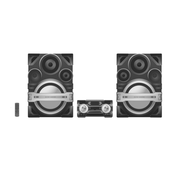
SB-MAX500 L
Please refer to the original service manual for:
CD Mechanism Unit, Order No. PSG1201019AE
Speaker system SB-MAX500LMK, Order No. PMX1302002CE
Nota: El idioma original de este Manual de Servicio es en idioma inglés, sin embargo algunas notasaquí mencionadas serán escritas
en español para mejor descripción para Centros de Servicio de México.
TABLE OF CONTENTS
SB-MAX500 R
SA-MAX500
SA-MAX500LMK
Model No.
Product Color: (K)...Black Type
© Panasonic Corporation 2013. All rights reserved.
Unauthorized copying and distribution is a violation
of law.
PMX1302001CE
CD Stereo System
Advertisement
Table of Contents

Related Manuals for Panasonic SA-MAX500LMK


Summary of Contents for Panasonic SA-MAX500LMK
-
Page 1: Table Of Contents
8.1. Cold-Start 2.4. Handling Precautions for Traverse Unit 2.5. Grounding electrostatic breakdown 8.2. Doctor Mode Table prevention 8.3. Reliability Test Mode (CD Mechanism Unit) © Panasonic Corporation 2013. All rights reserved. Unauthorized copying and distribution is a violation of law. - Page 2 15.2. FL Display & Volume P.C.B. 15.3. Control, Mic, USB, Remote Sensor. 8.4. Self-Diagnostic Mode 8.5. Self-Diagnostic Error Code Table 15.4. SMPS 8.6. Sales Demonstration Lock Function 15.5. Control Jog LED, Volume Jog LED & CD 9 Troubleshooting Guide Interface P.C.B. 10 Disassembly and Assembly Instructions 16 Appendix Information of Schematic Diagram 10.1.
-
Page 3: Safety Precautions
1 Safety Precautions 1.1. General Guidelines 1. IMPORTANT SAFETY NOTICE There are special components used in this equipment which are important for safety. These parts are marked by in the Schematic Diagrams, Circuit Board Layout, Exploded Views and Replacement Parts List. It is essential that these critical parts should be replaced with manufacturer’s specified parts to prevent X-RADIATION, shock, fire, or other hazards. -
Page 4: Before Repair And Adjustment
1.3. Before Repair and Adjustment Disconnect AC power to discharge the AC Capacitors (C5700, C5701, C5702, C5703, C5704, C5705, C5706, C5707, C5708) through a 10 Ω, 10 W resistor to ground. Caution: DO NOT SHORT-CIRCUIT DIRECTLY (with a screwdriver blade, for instance), as this may destroy solid state devices. After repairs are completed, restore power gradually using a variac, to avoid overcurrent. -
Page 5: Safety Parts Information
Schematic Diagrams, Exploded View & Replacement Parts List. It is essential that these critical parts should be replaced with manufacturer’s specified parts to prevent shock, fire or other hazards. Do not modify the original design without permission of manufacturer. Panasonic de México S.A. de C.V. Ingeniería de Audio SC-MAX500LMK... -
Page 6: Warning
2 Warning 2.1. Prevention of Electrostatic Discharge (ESD) to Electrostatically Sensi- tive (ES) Devices Some semiconductor (solid state) devices can be damaged easily by static electricity. Such components commonly are called Elec- trostatically Sensitive (ES) Devices. The following techniques should be used to help reduce the incidence of component damage caused by electrostatic discharge (ESD). -
Page 7: Precaution Of Laser Diode
2.2. Precaution of Laser Diode Caution: This product utilizes a laser diode with the unit turned “on”, invisible laser radiation is emitted from the pickup lens. Wavelength: 790 nm (CD) Maximum output radiation power from pickup: 100 μW/VDE Laser radiation from the pickup unit is safety level, but be sure the followings: 1. -
Page 8: Service Caution Based On Legal Restrictions
2.3. Service caution based on Legal restrictions 2.3.1. General description about Lead Free Solder (PbF) The lead free solder has been used in the mounting process of all electrical components on the printed circuit boards used for this equipment in considering the globally environmental conservation. The normal solder is the alloy of tin (Sn) and lead (Pb). -
Page 9: Handling Precautions For Traverse Unit
2.4. Handling Precautions for Traverse Unit The laser diode in the optical pickup unit may break down due to static electricity of clothes or human body. Special care must be taken avoid caution to electrostatic breakdown when servicing and handling the laser diode in the traverse unit. Cautions to Be Taken in Handling the Optical Pickup Unit 2.4.1. -
Page 10: Grounding For Electrostatic Breakdown Prevention
2.5. Grounding for electrostatic breakdown prevention • As for parts that use optical pick-up (laser diode), the optical pick-up is destroyed by the static electricity of the working environ- ment. Repair in the working environment that is grounded. 2.5.1. Worktable grounding •... -
Page 11: Service Navigation
3 Service Navigation 3.1. Service Information This service manual contains technical information which will allow service personnel’s to understand and service this model. Please place orders using the parts list and not the drawing reference numbers. If the circuit is changed or modified, this information will be followed by supplement service manual to be filed with original service manual. -
Page 12: Firmware Update Procedure
3.2. Firmware Update Procedure Start Write encrypted UPD bin to CD-R Turn On main set Insert CD-R (with UPD bin) and close TOC reading "CHECKING" "NO PLAY" process end Writing starts: "0%" -> "20%" -> "40%" -> "60%" -> "80%" -> 100%" "GOOD"... -
Page 13: Specifications
4 Specifications Especificaciones Salida de audio (disco) Número de canales 2,2 ch (FL, FR, SW) FL = Canal frontal izquierdo FR = Canal frontal derecho Sección del amplificador SW = Canal de subwoofer MPEG-1 Layer 3 Potencia de salida RMS en modo estéreo Alto (ambos controlados por los canales) 250 W por canal (5 ), 1 kHz, 30% THD Sección de memoria interna... -
Page 14: General/Introduction
5 General/Introduction 5.1. Media Information... -
Page 15: Location Of Controls And Components
6 Location of Controls and Components 6.1. Remote Control Key Button Operation SLEEP PLAY/ Configurar el temporizador de apagado automático AUTO OFF Apagar automáticamente el sistema Mientras la fuente sea el disco, el dispositivo USB o de memoria interna, la función de apagado automático apagará... -
Page 16: Main Unit Key Button Operation
6.2. Main Unit Key Button Operation Interruptor de alimentación en espera/conectada Configurar el temporizador de apagado automático Bandeja de disco Apagar automáticamente el sistema Pulse este interruptor para cambiar del modo de Mientras la fuente sea el disco, el dispositivo USB o de Toma puerto de música alimentación conectada al modo de alimentación en memoria interna, la función de apagado automático... -
Page 17: Installation Instructions
7 Installation Instructions 7.1. Speaker and A/C Connection Cómo realizar las conexiones Conecte el cable de alimentación de sólo después de haber hecho todas las demás conexiones. Corriente alterna = Para México: ca ó Vca Símbolo universal: ∼ En este instructivo nos referiremos a la corriente ∼... -
Page 18: Service Mode
8 Service Mode 8.1. Cold-Start Here is the procedure to carry out cold-start or initialize to shipping mode. 1. Unplug AC power cord 2. Press & hold [POWER] button 3. Plug AC power cord while [POWER] button being pressed FL Display will show “_ _ _ _ _ _ _ _” 4. - Page 19 8.2. Doctor Mode Table 8.2.1. Doctor Mode Table 1 Item Key Operation FL Display Mode Name Description Front Key Doctor Mode 1. Press [ ] button on main unit follow by [4] and [7] on remote control. 2. To exit, press [DELETE] button on remote control or, press [POWER, /I] button on Main Unit...
-
Page 20: Doctor Mode Table 2
8.2.2. Doctor Mode Table 2 Item Key Operation FL Display Mode Name Description Front Key Volume Setting To check the volume setting of a main In Doctor Mode : Check unit. 1. Press [7], [8], [9] button on remote control. Press [7]: VOL50 Vo lume Press [8]: VOL35... - Page 21 8.2.3. Doctor Mode Table 3 Item Key Operation FL Display Mode Name Description Front Key i. Function: To display result of In Doctor Mode: Self- Adjustment self-adjustment for CD . 1. Press [10] [1] [4] button on remote control . (AJST) This is used for servicing Result Display...
-
Page 22: Reliability Test Mode (Cd Mechanism Unit)
8.3. Reliability Test Mode (CD Mechanism Unit (BRS11C)) Below is the process flow chart of the aging test for the CD Mechanism Unit (BRS11C). OPEN First Track Operation Access OPEN wait First Track for 1 s Play 5 s CLOSE Count up Last Track Operation... -
Page 23: Self-Diagnostic Mode
8.4. Self-Diagnostic Mode Item Key Operation FL Display Mode Name Description Front Key Self Diagnostic To enter into self diagnostic checking Step 1: Select CD mode Mode (Ensure no disc is inserted). Step 2: Press & hold [ ] button follow by [ ] on main unit for 2 seconds. -
Page 24: Sales Demonstration Lock Function
8.5.2. CD Mechanism Error Code Table (CD Mechanism Unit) Error Code Diagnostic Contents Description of error Automatic FL Display Remarks CD H15 CD Open Abnormal During operation Press [ ] on main unit for POS_SW_R On fail to be next error. detected with 4 sec. -
Page 25: Troubleshooting Guide
9 Troubleshooting Guide 9.1. Part Location 9.1.1. SMPS P.C.B. AC Inlet : P5701 Fuse : SMPS Control IC : Photocoupler : IC5799 PC5702, PC5799 Switching Regulator IC : Thermistor : IC5701 Sub Transformer : TH5861 D5798 Sub Transformer : T5751 Rectifier Diode : D5801, D5802 Photocoupler :... - Page 26 9.1.2. Main P.C.B. (Front Side) Regulator Circuit IC2014 Fig. 2 Main P.C.B. (Front Side)
- Page 27 Fig. 3 Main P.C.B. (Back Side)
- Page 28 9.1.3. D-AMP P.C.B. Resistor Defective Resistor Defective Resistor Defective Resistor Defective Resistor Defective Resistor Defective R5405 R5005 R5201 R5305 Resistor Defective Resistor Defective Resistor Defective Resistor Defective Resistor Defective R5410 R5402 R5004 R5200 R5302 Resistor Defective Resistor Defective Resistor Defective R5011 R5211 R5311...
- Page 29 9.2. Troubleshooting Guide for F61 and/or F76 This section illustrates the checking procedures when upon detecting the error of “F61” and/or “F76” after power up of the unit. It is for purpose of troubleshooting and checking in SMPS, Main & D-Amp P.C.B.. Symptom Checking Items Possible Fault(s)
- Page 30 9.3. D-Amp IC Operation & Control (MAX500)
- Page 31 1170 ~ 1250 1260 ~ 1450 1460 ~ 1540 1550 ~ 1710 Table 4: F_HOP Control during 10 kHz Step Note: During activating, the 3 control pins namely MUTE_F, MUTE_A and MODE_DA must be used to cover the “Pop” sound cause by F-HOP switching.
- Page 32 Service Fixture & Tools Prepare service tools before process service position. Ref. No Service Tools Remarks SFT1 Main P.C.B. (CN2007) - SMPS P.C.B. (CN5802) REX1552(15P Cable Wire)
-
Page 33: Disassembly And Assembly Instructions
10 Disassembly and Assembly Instructions Caution Note: This section describes the disassembly and/or assembly procedures for all major printed circuit boards & main compo- nents for the unit. (You may refer to the section of “Main components and P.C.B Locations” as described in the service manual) Before carrying out the disassembly process, please ensure all the safety precautions &... -
Page 35: Disassembly Flow Chart
10.2. Disassembly Flow Chart 10.4. Top Cabinet 10.21. SMPS P.C.B. 10.5. Front Panel Unit 10.19. Main P.C.B. Voltage Regulator 10.22. Switching 10.14. Mic P.C.B. IC (IC2010) Regulator IC (IC5701) Voltage Regulator 10.23. Rectifier Diode 10.6. FL Display IC (IC2011) (D5702, D5801) P.C.B. -
Page 36: Main Components And P.c.b. Locations
10.3. Main Components and P.C.B. Locations SMPS P.C.B. -
Page 37: Disassembly Of Top Cabinet
10.4. Disassembly of Top Cabinet Step 5 Slightly lift up both side of Top Cabinet in an outward direction as shown. Step 1 Remove 3 screws. Step 6 Remove the Top Cabinet. Step 2 Remove 3 screws. Caution: During assembling, ensure that the catches of the Top Cabinet catches are properly located &... -
Page 38: Disassembly Of Front Panel Unit
10.5. Disassembly of Front Panel Step 7 Remove the Front Panel Unit Unit Front Panel Unit Refer to “Disassembly of Top Cabinet”. Step 1 Remove 1 screw at the SMPS P.C.B. Step 4 Detach 30P FFC at the connector (CN2003) on Main P.C.B.. -
Page 39: Disassembly Of Fl Display P.c.b
10.6. Disassembly of FL Display Caution: During assembling, ensure that the FL Display P.C.B. is properly located and fully catched onto Front P.C.B. Panel Unit. Refer to “Disassembly of Top Cabinet”. Refer to “Disassembly of Front Panel Unit”. Step 1 Remove 6 screws. Step 2 Release 4 catches. -
Page 40: Disassembly Of Control P.c.b
10.8. Disassembly of Control P.C.B. Step 4 Remove 4 screws. Step 5 From R part of P.C.B. Refer to “Disassembly of Top Cabinet”. Refer to “Disassembly of Front Panel Unit”. Refer to “Disassembly of FL Display P.C.B.”. Step 1 Remove the Control Knob. Step 2 Remove 2 screws. -
Page 41: Disassembly Of Volume P.c.b
10.10. Disassembly of Volume P.C.B. Step 7 Detach 12P Cable at a connector (CN6010) on the Con- trol P.C.B.. Refer to “Disassembly of Top Cabinet”. Refer to “Disassembly of Front Panel Unit”. Refer to “Disassembly of FL Display P.C.B.”. CN6010 Refer to “Disassembly of Control P.C.B.”. - Page 42 Step 2 Remove 2 screws. Step 9 Release catches by following the sequences (1-4). Step 3 Remove the Side Cover. Step 4 Remove 5 screws. Step 6 Detach 4P Cable at a connector (CN6005) on the LED P.C.B.. Step 8 Detach 8P Cable at a connector (CN6002) on the Mic P.C.B..
-
Page 43: Disassembly Of Volume Jog Led
10.11. Disassembly of Volume Jog 10.12. Disassembly of Remote Sensor LED P.C.B. P.C.B. Refer to “Disassembly of Top Cabinet”. Refer to “Disassembly of Top Cabinet”. Refer to “Disassembly of Front Panel Unit”. Refer to “Disassembly of Front Panel Unit”. Refer to “Disassembly of FL Display P.C.B.”. Refer to “Disassembly of FL Display P.C.B.”. -
Page 44: Disassembly Of Mic P.c.b
10.14. Disassembly of Mic P.C.B. 10.15. Disassembly of LED P.C.B. Refer to “Disassembly of Top Cabinet”. Refer to “Disassembly of Top Cabinet”. Refer to “Disassembly of Front Panel Unit”. Refer to “Disassembly of Front Panel Unit”. Step 1 Remove the Mic Knob. Step 1 Remove 2 screws. -
Page 45: Disassembly Of Cd Lid
10.16. Disassembly of CD Lid Step 2 Remove CD Lid as arrow shown. Step 3 Remove CD Lid from the guide. Refer to “Disassembly of Top Cabinet”. Refer to “Disassembly of Front Panel Unit”. Step 1 Remove the spring as arrow shown in order of sequence (1) to (3). -
Page 46: Disassembly Of Rear Panel
10.17. Disassembly of Rear Panel Step 5 Release 2 tabs. Step 6 Remove the Rear Panel. Refer to “Disassembly of Top Cabinet”. Step 1 Remove 9 screws. Step 3 Release catches on fans. Step 4 Remove 2 fans. -
Page 47: Disassembly Of Cd Mechanism Unit
10.18. Disassembly of CD Mecha- 10.19. Disassembly of Main P.C.B. nism Unit Refer to “Disassembly of Top Cabinet”. Refer to “Disassembly of Front Panel Unit”. Refer to “Disassembly of Top Cabinet”. Refer to “Disassembly of Rear Panel”. Refer to “Disassembly of Front Panel Unit”. Refer to “Disassembly of CD Mechanism Unit”. -
Page 48: Disassembly Of Smps P.c.b
10.21. Disassembly of SMPS P.C.B. Refer to “Disassembly of Top Cabinet”. Step 1 Remove 2 screws. Step 2 Detach 15P Cable at a connector (CN5802) on the SMPS P.C.B.. Step 3 Detach 2P Wire at a connector (CN2006) on the Main P.C.B.. - Page 49 Step 8 Remove the SMPS P.C.B.. Step 6 Remove 2 screws Step 7 Remove the Inner Fan Unit. Caution: During assembling, ensure that the SMPS P.C.B. Caution: Keep the Fan Fixtures in safe place, place it back is properly located & fully seated onto the Inner Chassis during assembling.
- Page 50 10.22. Replacement of Switching Reg- Step 3 Remove the Heatsink A with the Switching Regulator (IC5701).AA ulator (IC5701) Step 4 Remove 1 screw. Refer to “Disassembly of SMPS P.C.B.”. Step 5 Remove the Switching Regulator (IC5701) from the Heatsink A. 10.22.1.
- Page 51 10.22.2. Assembly of Switching Regulator Step 4 Solder pins of the Switching Regulator (IC5701) on the solder side of the SMPS P.C.B.. (IC5701) Step 5 Solder pins of the Heatsink A on the solder side of the Step 1 Apply grease to the Heatsink A. SMPS P.C.B..
-
Page 52: Replacement Of Rectifier Diode (D5801)
10.23. Replacement of Rectifier Diode Step 3 Remove 1 screw at Rectifier Diode (D5702). Step 4 Remove the Rectifier Diode (D5702) from the SMPS (D5702) P.C.B.. Refer to “Disassembly of SMPS P.C.B.”. Caution: Avoid touching the Heatsink B due to its high temperature after prolonged use. - Page 53 Step 4 Solder pins of the Rectifier Diode (D5702) on the solder 10.24. Replacement of Rectifier Diode side of the SMPS P.C.B.. (D5801) Step 5 Solder pins of the Heatsink A on the solder side of the SMPS P.C.B.. Refer to “Disassembly of SMPS P.C.B.”. 10.24.1.
-
Page 54: Disassembly Of Cd Interface P.c.b
Step 3 Remove 1 screw at Rectifier Diode (D5801). Step 4 Solder pins of the Rectifier Diode (D5801) on the solder Step 4 Remove the Rectifier Diode (D5801) from the SMPS side of the SMPS P.C.B.. P.C.B.. Step 5 Solder pins of the Heatsink B. Caution: Avoid touching the Heatsink B due to its high temperature after prolonged use. - Page 55 Replacement of Rectifier Diode Step 3 Remove 1 screw at Rectifier Diode (D5802). Step 4 Remove the Rectifier Diode (D5802) from the SMPS (D5802) P.C.B.. Refer to “Disassembly of SMPS P.C.B.”. Caution: Avoid touching the Heatsink B due to its high temperature after prolong use.
- Page 56 Step 4 Solder pins of the Rectifier Diode (D5802) on the solder Replacement of Regulator side of SMPS P.C.B.. Diode (D5803) Step 5 Solder pins of the Heatsink B.. Refer to “Disassembly of SMPS P.C.B.”. Disassembly of Rectifier Diode (D5803) Step 1 Desolder pins of the Rectifier Diode (D5803) on the sol- der side of SMPS P.C.B..
- Page 57 Step 3 Remove 1 screw at Rectifier Diode (D5803). Step 4 Solder pins of the Rectifier Diode (D5803) on the solder Step 4 Remove the Rectifier Diode (D5803) from SMPS P.C.B.. side of the SMPS P.C.B. Caution: Avoid touching the Heatsink B due to its high Step 5 Solder pins of the Heatsink B..
-
Page 58: Service Position
11 Service Position Note: For description of the disassembly procedures, see the Section 10. 11.1. Checking and Repairing of FL Step 13 Attach 8P Cable at a connector (CN6002) on the Mic Display P.C.B., Control P.C.B., P.C.B.. Volume P.C.B., Mic P.C.B. and Step 14 Attach 12P Cable at a connector (CN6010) on the Control P.C.B.. -
Page 59: Checking And Repairing Of Main P.c.b. (Side B)
11.2. Checking and Repairing of Main P.C.B. (Side B) Step 13 Attach 11P Cable at a connector (CN2700) on the Step 1 Remove Top Cabinet. Main P.C.B.. Step 2 Remove Front Panel Unit. Step 14 Attach 30P FFC at a connector (CN2003) on the Main Step 3 Remove Rear Panel. -
Page 60: Checking And Repairing Of Main P.c.b. (Side A)
11.3. Checking and Repairing of Main P.C.B. (Side A) Step 14 Attach Cable at a connector (CN2700) on the Step 1 Remove Top Cabinet. Main P.C.B.. Step 2 Remove Front Panel Unit. Step 15 Attach 30P FFC at a connector (CN2003) on the Main P.C.B.. - Page 61 11.4. Checking and Repairing of SMPS P.C.B. Step 1 Remove Top Cabinet. Step 2 Remove SMPS P.C.B.. Step 3 Attach 13P Cable at the connector (CN5802) on the SMPS P.C.B.. Step 4 Flip the SMPS P.C.B.. Step 5 Attach 2P Wire at the connector (CN2006) on the Main P.C.B..
-
Page 62: Block Diagram
12 Block Diagram 12.1. Servo & System Control : CD AUDIO INPUT SIGNAL LINE : AUDIO OUTPUT SIGNAL LINE : USB SIGNAL LINE CD SERVO P.C.B. MAIN P.C.B. USB P.C.B. IC8001 IC8051 MN6627992AB CN6301 USB PORT SERVO C3ABPG000163 64M SDRAM PROCESSOR VBUS 1 VBUS... - Page 63 : USB SIGNAL LINE : CD AUDIO INPUT SIGNAL LINE : AUDIO OUTPUT SIGNAL LINE MAIN P.C.B. IC2003 *MN101EF16KXW MICROPROCESSOR REMOTE SENSOR P.C.B. IR6200 REMOTE CONTROL SENSOR TO SERVO & SYSTEM CONTROL CN2003 CN6000 CN6001 CN6200 RMT 86 3.3V BLOCK (1/2) PANEL P.C.B.
-
Page 64: Ic Terminal Chart
12.2. IC Terminal Chart IC8051 IC8001 64M SDRAM SERVO PROCESSOR SIGNAL NAME PORT NAME PIN NO PIN NO PORT NAME IC8051 IC8001 64M SDRAM SERVO PROCESSOR SIGNAL NAME PORT NAME PIN NO PIN NO PORT NAME DQ0 / DQ15 2 / 53 DQ1 / DQ14 4 / 51 DQ2 / DQ13... -
Page 65: Audio
12.3. Audio : CD AUDIO INPUT SIGNAL LINE : AUX/TUNER/MUSIC PORT/MIC AUDIO INPUT SIGNAL LINE : AUDIO OUTPUT SIGNAL LINE : AM SIGNAL LINE : FM SIGNAL LINE MAIN P.C.B. IC2000 C1AB00003256 JK2000 AUX L 38 IN3B AUX IN AUX R 2 IN3A IC52 C1AB00003566... - Page 66 : CD AUDIO INPUT SIGNAL LINE : AUX/TUNER/MUSIC PORT/MIC AUDIO INPUT SIGNAL LINE : AUDIO OUTPUT SIGNAL LINE : AM SIGNAL LINE : FM SIGNAL LINE MAIN P.C.B. IC5800 C1BA00000497 AUDIO DIGITAL AMPLIFIER SPEAKERS FR L TWEETER 2 IN1+ BOOT1 FR L WOOFER JK5601 21 IN2-...
-
Page 67: Power Supply
12.4. Power Supply SMPS P.C.B. MAIN P.C.B. IC5799 MIP2F20MSSCF SWITCHING MODE POWER T5751 SUPPLY CONTROL TRANSFORMER CL 3 D5795 D5798 VCC 4 D5896 CN5802 SYS3.3V CN2007 SYS3.3V SYS3.3V D5793 IC5899 C0DAEYY00040 SHUNT PC5799 REGULATOR TO POWER SUPPLY FEEDBACK BLOCK (2/2) FB 2 VDD 1 CN5802... -
Page 68: Wiring Connection Diagram
13 Wiring Connection Diagram CD INTERFACE P.C.B. USB P.C.B. (SOLDER SIDE) (SOLDER SIDE) FP8251 USB PORT 10 9 SMPS P.C.B. CN5801 M7302* (SOLDER SIDE) CN6301 (SPINDLE MOTOR) T5701 (MAIN TRANSFORMER) FP8201 ZJ6300* 4 5 6 7 CD SERVO P.C.B. CN7002 9 10 (SIDE B) TO OPTICAL PICKUP UNIT... -
Page 69: Schematic Diagram
14 Schematic Diagram Voltage and signal line : +B signal line : -B signal line 16.1. Schematic Diagram Notes : CD Audio input signal line : AUX/Tuner/Music Port/Mic Audio input signal line This schematic diagram may be modified at any time : Audio output signal line with the development of new technology. - Page 70 14.2. CD Servo Circuit SCHEMATIC DIAGRAM - 1 CD SERVO CIRCUIT : +B SIGNAL LINE : CD AUDIO INPUT SIGNAL LINE : AUDIO OUTPUT SIGNAL LINE : USB SIGNAL LINE 84 83 76 75 68 67 65 64 59 58 46 45 C8503 VCCQ...
- Page 71 SCHEMATIC DIAGRAM - 2 CD SERVO CIRCUIT : +B SIGNAL LINE : CD AUDIO INPUT SIGNAL LINE : AUDIO OUTPUT SIGNAL LINE : USB SIGNAL LINE R8014 NCSSF R8013 IO1SF R8012 IO2SF C8401 C8403 0.01 IC8401 C9006 C3FBMY000303 PW_+5V 16M FLASH MEMORY DGND R8015 IO0SF...
- Page 72 SCHEMATIC DIAGRAM - 3 CD SERVO CIRCUIT : +B SIGNAL LINE : CD AUDIO INPUT SIGNAL LINE : AUDIO OUTPUT SIGNAL LINE : USB SIGNAL LINE TO CD SERVO CIRCUIT (1/4) C8076 LB8402 R8032 J0JHC0000045 PW_3R3V_MAIN R8031 CKA134 C8050 R9005 R8047 CKA138 30 29...
- Page 73 SCHEMATIC DIAGRAM - 4 CD SERVO CIRCUIT : +B SIGNAL LINE : CD AUDIO INPUT SIGNAL LINE : AUDIO OUTPUT SIGNAL LINE : USB SIGNAL LINE TO CD SERVO CIRCUIT (2/4) FP8251 TRV+ TRV- LDM+ IC8301 LDM- C0FBAK000026 CD INTERFACE OPEN_SW DIGITAL AUDIO LB8301...
- Page 74 Main(Micon) Circuit SCHEMATIC DIAGRAM - 5 : +B SIGNAL LINE : CD AUDIO INPUT SIGNAL LINE : AUDIO OUTPUT SIGNAL LINE : FM SIGNAL LINE MAIN(MICON) CIRCUIT : -B SIGNAL LINE : AUX/TUNER/MUSIC PORT/MIC AUDIO INPUT SIGNAL LINE : AM SIGNAL LINE : USB SIGNAL LINE C2067 Q2040...
- Page 75 SCHEMATIC DIAGRAM - 6 : +B SIGNAL LINE : CD AUDIO INPUT SIGNAL LINE : AUDIO OUTPUT SIGNAL LINE : FM SIGNAL LINE MAIN(MICON) CIRCUIT : -B SIGNAL LINE : AUX/TUNER/MUSIC PORT/MIC AUDIO INPUT SIGNAL LINE : AM SIGNAL LINE : USB SIGNAL LINE TO MAIN(MICON) CIRCUIT (3/10)
- Page 76 SCHEMATIC DIAGRAM - 7 : +B SIGNAL LINE : CD AUDIO INPUT SIGNAL LINE : AUDIO OUTPUT SIGNAL LINE : FM SIGNAL LINE MAIN(MICON) CIRCUIT : -B SIGNAL LINE : AUX/TUNER/MUSIC PORT/MIC AUDIO INPUT SIGNAL LINE : AM SIGNAL LINE : USB SIGNAL LINE TO MAIN(MICON) CIRCUIT (2/10)
- Page 77 SCHEMATIC DIAGRAM - 8 : +B SIGNAL LINE : CD AUDIO INPUT SIGNAL LINE : AUDIO OUTPUT SIGNAL LINE : FM SIGNAL LINE MAIN(MICON) CIRCUIT : -B SIGNAL LINE : AUX/TUNER/MUSIC PORT/MIC AUDIO INPUT SIGNAL LINE : AM SIGNAL LINE : USB SIGNAL LINE R2205 4.7K...
- Page 78 SCHEMATIC DIAGRAM - 9 : +B SIGNAL LINE : CD AUDIO INPUT SIGNAL LINE : AUDIO OUTPUT SIGNAL LINE : FM SIGNAL LINE MAIN(MICON) CIRCUIT : -B SIGNAL LINE : AUX/TUNER/MUSIC PORT/MIC AUDIO INPUT SIGNAL LINE : AM SIGNAL LINE : USB SIGNAL LINE R2089 C2113...
- Page 79 SCHEMATIC DIAGRAM - 10 : +B SIGNAL LINE : CD AUDIO INPUT SIGNAL LINE : AUDIO OUTPUT SIGNAL LINE : FM SIGNAL LINE MAIN(MICON) CIRCUIT : -B SIGNAL LINE : AUX/TUNER/MUSIC PORT/MIC AUDIO INPUT SIGNAL LINE : AM SIGNAL LINE : USB SIGNAL LINE TO MAIN(MICON) CIRCUIT (1/10)
- Page 80 SCHEMATIC DIAGRAM - 11 : +B SIGNAL LINE : CD AUDIO INPUT SIGNAL LINE : AUDIO OUTPUT SIGNAL LINE : FM SIGNAL LINE MAIN(MICON) CIRCUIT : -B SIGNAL LINE : AUX/TUNER/MUSIC PORT/MIC AUDIO INPUT SIGNAL LINE : AM SIGNAL LINE : USB SIGNAL LINE TO MAIN(MICON) CIRCUIT (2/10)
- Page 81 SCHEMATIC DIAGRAM - 12 : +B SIGNAL LINE : CD AUDIO INPUT SIGNAL LINE : AUDIO OUTPUT SIGNAL LINE : FM SIGNAL LINE MAIN(MICON) CIRCUIT : -B SIGNAL LINE : AUX/TUNER/MUSIC PORT/MIC AUDIO INPUT SIGNAL LINE : AM SIGNAL LINE : USB SIGNAL LINE TO MAIN(MICON) CIRCUIT (3/10)
- Page 82 SCHEMATIC DIAGRAM - 13 : +B SIGNAL LINE : CD AUDIO INPUT SIGNAL LINE : AUDIO OUTPUT SIGNAL LINE : FM SIGNAL LINE MAIN(MICON) CIRCUIT : -B SIGNAL LINE : AUX/TUNER/MUSIC PORT/MIC AUDIO INPUT SIGNAL LINE : AM SIGNAL LINE : USB SIGNAL LINE TO MAIN(MICON) CIRCUIT (4/10)
- Page 83 SCHEMATIC DIAGRAM - 14 : +B SIGNAL LINE : CD AUDIO INPUT SIGNAL LINE : AUDIO OUTPUT SIGNAL LINE : FM SIGNAL LINE MAIN(MICON) CIRCUIT : -B SIGNAL LINE : AUX/TUNER/MUSIC PORT/MIC AUDIO INPUT SIGNAL LINE : AM SIGNAL LINE : USB SIGNAL LINE TO MAIN(MICON) CIRCUIT (5/10)
-
Page 84: Fl Display Circuit
14.3.FL Display Circuit MAX500... -
Page 85: Volume Circuit
14.4.Volume Circuit MAX500... -
Page 86: Control & Usb Circuit
14.5.Control & USB Circuit MAX500... -
Page 87: Remote Sensor
14.7. Remote Sensor MAX500... - Page 88 MAX500...
- Page 89 .Jog Board MAX500...
- Page 90 Internal Fan MAX500...
-
Page 91: Smps Circuit
14.8. SMPS Circuit SCHEMATIC DIAGRAM - 25 SMPS CIRCUIT : +B SIGNAL LINE : -B SIGNAL LINE CN5801 +35V_SENSE +35V_SENSE D-AMP CIRCUIT SYS_GND (ZJ5500*) SYS_GND IN SCHEMATIC -35V_SENSE DIAGRAM - 23 -35V_SENSE TO SMPS CIRCUIT (2/2) R5701 CN5802 220K SMPS_ID PCONT PCONT PW_DC+16V... - Page 92 SCHEMATIC DIAGRAM - 26 SMPS CIRCUIT : +B SIGNAL LINE : -B SIGNAL LINE TO SMPS CIRCUIT (1/2) L5701 R5708 C5701 G0B932H00002 P5701 ERJ8GEYJ155V F0CAF224A105 T8AH 250V 1.5M 0.22 ZA5701 ZA5702 AC IN DZ5701 ERZVA5Z471 ~127V 60Hz R5709 C5705 C5704 ERJ8GEYJ155V F1BAF471A013 F1BAF471A013...
-
Page 93: Printed Circuit Board
15 Printed Circuit Board 15.1. Main P.C.B. MAIN P.C.B. (RD-DAK110-PX) (SIDE A) SA-MAX500 MAIN P.C.B. - Page 94 MAIN P.C.B. (RD-DAK110-PX) (SIDE B) SA-MAX500 MAIN P.C.B.
- Page 95 COMPONENTES DE PISTA MAIN PSG Name & Description Ref. No. Parts No. RD-DAK110-PX MAIN PCB (completa con componentes) REP4768R CONJUNTO MANUAL MAIN RJB3542C TARJETA MAIN SIN COMPONENTES F1H1H102A219 GRM188B11H102KA01D F1H1A474A107 CL10B474KP8NNPC F1H1H120A230 GRM1882C1H120JD01D F1H1H120A230 GRM1882C1H120JD01D F1H1A105A025 LMK107BJ105KA-T F1H1A105A025 LMK107BJ105KA-T F1G1C104A077 GRM155B31C104KA87D F1G1C104A077 GRM155B31C104KA87D...
- Page 96 C2076 F1H1H104B047 CL10B104KB8NNPC C2077 F1H1H104B047 CL10B104KB8NNPC C2078 F1H1H473A783 C1608JB1H473KT C2079 F1H1H473A783 C1608JB1H473KT C2080 F1H1A334A028 C1608JB1A334KT000N C2081 F1H1A334A028 C1608JB1A334KT000N C2082 F1H1H332A013 CM105W5R332K50AT C2083 F1H1H223A219 GRM188B11H223KA01D C2084 F1H1C823A001 CM105W5R823K16AT C2085 F2A1H3R3A213 SM3R3M050B070T050P C2086 F2A1H3R3A213 SM3R3M050B070T050P C2087 F1H0J4750004 GRM188B30J475KE18D C2088 F1H1C823A001 CM105W5R823K16AT C2089 F2A1H3R3A213 SM3R3M050B070T050P C2090...
- Page 97 C2187 F1H1H103A219 GRM188B11H103KA01D C2188 F2A1A330B138 GS330M010C110T050P C2189 F1H1C104A042 GRM188B11C104KA01D... C2190 F2A1C221B456 GS221M016E110T050P C2191 F1H1H103A219 GRM188B11H103KA01D C2192 F1H0J105A051 CL10X105KQ8NNPC C2193 F1H0J105A051 CL10X105KQ8NNPC C2194 F1H1H103A219 GRM188B11H103KA01D C2196 F2A0J101A181 UVR0J101MDA1TA C2198 F2A1C102A019 RE3-16V102MG-T2 C2199 F1H1A225A051 GRM188B31A225KE33D C2200 F2A1E2210093 SK221M025F070T050P C2201 F1H1H103A219 GRM188B11H103KA01D C2202 D0GBR00J0004 RM06JTN0 C2204...
- Page 98 IC52 C1AB00003566 SI4730-D60-GMR IC2000 C1AB00003256 NJW1201AFH2 IC2001 C0ABBB000067 BA4558F-E2 IC2002 C0ABBB000067 BA4558F-E2 IC2003 MN101EF16KXW MICROPROCESADOR sin programar (genérico) IC2003 RFKWMAKX500M0 MICROPROCESADOR para uso de centros de servicio IC2004 C0ABBB000067 BA4558F-E2 IC2005 C0AABB000125 NJM4565D IC2006 C3EBEY000037 CAT24C04WI-GT3JN IC2008 C0DBZYY00311 BD2224G-TR IC2010 C0DAAYG00001 BD9873CP-V5E2 IC2011...
- Page 99 ERJ3GEYJ102V ERJ3GEYJ102V ERJ3GEYJ102V ERJ3GEYJ102V ERJ2GEJ472X ERJ2GEJ472X ERJ2GEJ472X ERJ2GEJ472X ERJ2GEJ221X ERJ2GEJ221X ERJ3GEYJ221V ERJ3GEYJ221V ERJ2GEJ102X ERJ2GEJ102X ERJ3GEYJ222V ERJ3GEYJ222V ERJ3GEYJ473V ERJ3GEYJ473V ERJ3GEYJ473V ERJ3GEYJ473V D0GBR00J0004 RM06JTN0 R2001 D0GB123JA065 RM06JTN123 R2002 D0GB123JA065 RM06JTN123 R2003 ERJ3GEYJ392V ERJ3GEYJ392V R2004 ERJ3GEYJ392V ERJ3GEYJ392V R2005 ERJ3GEYJ103V ERJ3GEYJ103V R2006 ERJ3GEYJ103V ERJ3GEYJ103V R2007 ERJ3GEYJ332V ERJ3GEYJ332V...
- Page 100 R2072 ERJ3GEY0R00V ERJ3GEY0R00V R2073 ERJ3GEYJ104V ERJ3GEYJ104V R2074 ERJ3GEYJ473V ERJ3GEYJ473V R2075 ERJ3GEYJ473V ERJ3GEYJ473V R2076 ERJ3GEYJ102V ERJ3GEYJ102V R2077 ERJ3GEYJ102V ERJ3GEYJ102V R2078 ERJ3GEYJ563V ERJ3GEYJ563V R2079 D0AF330JA039 RDF50SJR330 R2082 ERJ3GEYJ104V ERJ3GEYJ104V R2083 ERJ3GEYJ473V ERJ3GEYJ473V R2084 D0GB103JA065 RM06JTN103 R2085 D0GB332JA065 RM06JTN332 R2087 ERJ3GEY0R00V ERJ3GEY0R00V R2089 D0GB103JA065 RM06JTN103 R2093...
- Page 101 R2167 D0GB222JA065 RM06JTN222 R2171 D0GB473JA065 RM06JTN473 R2173 ERJ3GEYJ153V ERJ3GEYJ153V R2174 ERJ3GEYJ103V ERJ3GEYJ103V R2176 ERJ3RBD152V ERJ3RBD152V R2177 ERJ3GEYJ153V ERJ3GEYJ153V R2178 ERJ3GEYJ103V ERJ3GEYJ103V R2179 D0GB123JA065 RM06JTN123 R2180 D0GB104JA065 RM06JTN104 R2182 ERJ3GEYJ103V ERJ3GEYJ103V R2184 D0GB473JA065 RM06JTN473 R2185 ERJ3GEYJ103V ERJ3GEYJ103V R2189 ERJ3GEYJ473V ERJ3GEYJ473V R2192 ERJ3RBD102V ERJ3RBD102V R2193...
- Page 102 R2335 ERJ3GEYJ102V ERJ3GEYJ102V R2336 ERG2SJ471E ERG2SJ471E R2337 ERG2SJ471E ERG2SJ471E R2338 ERG2SJ471E ERG2SJ471E R2339 ERG2SJ471E ERG2SJ471E R2340 ERG2SJ471E ERG2SJ471E R2341 ERG2SJ471E ERG2SJ471E R2343 ERJ3GEY0R00V ERJ3GEY0R00V R2344 ERJ3GEYJ332V ERJ3GEYJ332V R2345 ERJ3GEYJ332V ERJ3GEYJ332V R2346 D0GB472JA065 RM06JTN472 R2347 D0GB472JA065 RM06JTN472 R2348 D0GB822JA065 RM06JTN822 R2349 ERJ3GEYJ104V ERJ3GEYJ104V R2350...
- Page 103 R2433 D0GBR00J0004 RM06JTN0 R2434 D0GB682JA065 RM06JTN682 R2435 D0GB152JA065 RM06JTN152 R2436 D0GB153JA065 RM06JTN153 R2438 D0GB682JA065 RM06JTN682 R2439 D0GB153JA065 RM06JTN153 R2440 D0GB152JA065 RM06JTN152 R2442 ERJ3GEYJ473V ERJ3GEYJ473V R2443 ERJ3GEYJ392V ERJ3GEYJ392V VA51 EZAEG2A50AX EZAEG2A50AX H0A327200181 CFS-20632768EZFB X2000 H0A327200181 CFS-20632768EZFB X2001 H2B800400007 CSTLS8M00G56-A0 ZJ2000 K9ZZ00001279 MET37-0005 ZJ2007 REX1552...
- Page 104 Printed Circuit Board 15.1.1 CD Servo P.C.B. CD SERVO P.C.B. (REP4749B) R8012 IC8401 R8013 C8513 R8014 FP8251 C8054 C8508 C8503 C8056 C8403 R8505 R8506 R8507 C8036 C8029 C8035 R8504 R8039 IC8501 3635 R8302 R8251 IC8051 R8301 C8509 R8264 R8502 R8042 FP8201 R8025 R8046...
- Page 105 . Panel, Remote Sensor, USB and Music Port P.C.B. PANEL P.C.B. (REPM12X2053A ) REMOTE SENSOR P.C.B. (REPM12X2053A ) IR6200 SENSOR CN6200 C6202 3543AB-2 3543AB-2 USB P.C.B. (REPM12X2053A ) USB PORT CN6301 D6300 ZJ6300* 3543AC-2 3543AC-2 MUSIC PORT P.C.B. (REPM12X2053A ) 3543AD-2 3543AD-2 JK6401...
- Page 106 15.2. Memory LED, CD Interface, Top Bar LED, Bottom Bar LED and Mic P.C.B. MEMORY LED P.C.B. (REPM12X2053A) TOP BAR LED P.C.B. (REPM12X953A) ZJ6800* D6600 D6601 D6602 R6601 R6600 3543AH-2 3543AH-2 D6800 ZJ6600* 3543AF-2 3543AF-2 CD INTERFACE P.C.B. (REPM12X2053A) BOTTOM BAR LED P.C.B. (REPM12X2053A) M7302* (SPINDLE MOTOR)
- Page 107 15.3 D-Amp P.C.B. D-AMP P.C.B. (REPM12X2051A) W5048 R5506 C5553 D5501 R5507 R5504 X5501 X5500 C5557 C5550 C5558 W5071 D5503 C5559 W5036 R5505 R5515 W5780 IC5500 R5513 W5033 K5301 K5202 C5117 C5000 W5044 W5032 C5221 C5001 W5004 C5315 C5106 R5005 R5004 C5234 R5201 R5200...
-
Page 108: Smps
15.4. SMPS SMPS P.C.B. (REPM12X2050A) Q5722 C5728 D5721 C5721 C5722 R5728 C5726 D5724 L5704 R5729 IC5701 D5727 R5723 Q5720 Q5721 C5702 R5710 D5701 K1...PH PC5701 HEATSINK D5702 Q5700 R5715 R5712 R5702 W5516 W5524 CN5801 C5712 W5906 R5726 C5713 C5737 R5714 T5701 R5727 (MAIN TRANSFORMER) -
Page 109: Control Jog Led, Volume Jog Led & Cd Interface P.c.b
15.5. CD Interface P.C.B. CD INTERFACE P.C.B. (REP4755A) M7302* (SPINDLE MOTOR) S7201 (RESET) CN7002 CN7001 M7301* TO LOADING P.C.B. (TRAVERSE (CD MECHANISM MOTOR) UNIT BRS11C) 3556A 3556A NOTE: " * " REF IS FOR INDICATION ONLY SA-MAX500 CONTROL JOG LED / VOLUME JOG LED / CD INTERFACE P.C.B. -
Page 110: Appendix Information Of Schematic Diagram
18 Appendix Information of Schematic Diagram 18.1. Voltage & Waveform Chart Note: • Indication Voltage Values are in standard values for the unit measured by the DC electronic circuit tester (high-impedance) with the chassis taken as standard. Therefore, there may exist some errors in voltage values, depending on the internal impedance of the DC circuit tester. •... - Page 111 18.1.2. CD Servo P.C.B. (2/3) IC8251 REF NO. MODE CD PLAY REF NO. IC8301 MODE CD PLAY REF NO. IC8401 MODE CD PLAY REF NO. IC8501 MODE CD PLAY REF NO. IC8501 MODE CD PLAY REF NO. IC8501 MODE CD PLAY REF NO.
- Page 112 18.1.4. Main P.C.B. (1/4) IC52 REF NO. MODE TUNER REF NO. IC2000 MODE POWER ON STANDBY REF NO. IC2000 MODE POWER ON STANDBY REF NO. IC2000 MODE POWER ON STANDBY REF NO. IC2001 MODE POWER ON 16.0 STANDBY 16.0 REF NO. IC2002 MODE POWER ON...
- Page 113 18.1.5. Main P.C.B. (2/4) IC2003 REF NO. MODE POWER ON STANDBY IC2004 REF NO. MODE POWER ON 17.1 17.0 TUNER 17.1 17.0 IC2005 REF NO. MODE CD PLAY 17.8 STANDBY 17.8 IC2006 REF NO. MODE POWER ON STANDBY REF NO. IC2008 MODE POWER ON...
- Page 114 18.1.6. Main P.C.B. (3/4) REF NO. Q2000 Q2001 Q2002 Q2003 Q2004 MODE CD PLAY 15.0 STANDBY 15.0 REF NO. Q2005 Q2006 Q2007 Q2008 Q2009 MODE CD PLAY STANDBY REF NO. Q2010 Q2011 Q2016 Q2017 Q2020 MODE CD PLAY 18.2 STANDBY 18.2 REF NO.
- Page 115 18.1.7. Main P.C.B. (4/4) REF NO. Q5603 Q5604 MODE CD PLAY STANDBY Q2018 Q2022 Q2024 REF NO. Q2025 Q2027 MODE POWER ON STANDBY REF NO. Q2018 Q2022 Q2024 Q2025 Q2027 MODE POWER ON STANDBY REF NO. Q2031 Q2033 Q5600 Q5601 Q5602 MODE POWER ON...
- Page 116 18.1.9. D-Amp P.C.B. REF NO. IC5000 MODE POWER ON -34.1 -28.5 37.3 -37.3 -27.2 -37.3 37.3 -37.1 -37.1 STANDBY -34.1 -28.5 37.3 -37.3 -27.2 -37.3 37.3 -37.1 -37.1 REF NO. IC5000 MODE POWER ON STANDBY REF NO. IC5200 MODE POWER ON -34.1 -28.6 37.3 -37.4 -27.2 -37.4 37.3 -37.1 -37.1...
- Page 117 18.1.10. SMPS P.C.B. REF NO. IC5701 MODE POWER ON 164.8 19.1 STANDBY 164.8 19.1 REF NO. IC5799 MODE POWER ON 11.0 164.2 STANDBY 11.0 164.2 REF NO. IC5801 MODE POWER ON -30.0 STANDBY -30.0 REF NO. IC5899 MODE POWER ON STANDBY REF NO.
- Page 118 18.1.12. Waveform Table 0.1Vp-p(200usec/div) 0.48Vp-p(1usec/div) 2Vp-p(200usec/div) 0.48Vp-p(1usec/div) 1.1Vp-p(50usec/div) 4Vp-p(50nsec/div) 3Vp-p(10usec/div) 0.52Vp-p(1usec/div) 44Vp-p(1usec/div) 2Vp-p(1usec/div) 44Vp-p(1usec/div) 2Vp-p(1usec/div) 0.5Vp-p(2usec/div) 2.5Vp-p(200usec/div) 0.4Vp-p(5usec/div) 2Vp-p(200usec/div) 0.4Vp-p(1usec/div)
-
Page 119: Illustration Of Ics, Transistor And Diode
18.2. Illustration of ICs, Transistor and Diode *Este material se encuentra sin programar, debe ser programado. C0ABBB000067 (8P) C0FBAK000026(16P) C0HBB0000057 (44P) C0DBEYY00123 (8P) C1BA00000497 (23P) C1AB00003566 (20P) C1AB00003130 (14P) C3FBYY000034 (169P) C3FBMY000303 (8P) C0JBAB000902 (14P) C1ZBZ0004646 (8P) C3ABPG000163(54P) No.1 No.1 No.1 No.1 No.1... -
Page 120: Terminal Function Of Ics
18.3. Terminal Function of ICs 18.3.1. IC2003 (*MN101EF16KXW): Terminal Name Function MICRO-PROCESSOR CLOSE_SW CD Close Switch Detection CD_OPEN_SW CD Open Switch Detection CD_RESET_SW CD Reset Detection Terminal Name Function LOAD_CCW Loading Motor Turning Counter-Clockwise (Tray CLIP ATTN Clipping attenuation Close) ASP_DATA ASP data LOAD_CW... -
Page 121: Exploded View And Replacement Parts List
17 Exploded View and Replacement Parts List 17.1. Exploded View and Mechanical replacement Part List Cabinet Parts Location 17.1.1. Mem Button L Lighting Button USB PCB FL Filter Sheet Display PCB Side Cover Rotary Jog PCB Volume Jog PCB FL Window Mem Button R Vol Light Reflector... - Page 122 Top Cabinet SOPORTE fAN CHASSIS de Mecanismo RHD30007-K2J (35) RMZ1358 RHDX031008 (38) Jack (BRS1C) Ventilador Rear Panel (MAIN P.C.B.) Traverse Deck RHD30119-S (37) RHDX30005-J (39) Fan Fixure CN7002 G4DYZ0000062 CN7001 S7201 RHD26046 (34) PCB SPACER (49) IC INSULATOR RHD30111-31 (36) (SMPS P.C.B.) Ventilador Mecha support...
- Page 123 17.1.2. Packaging ACCESSORIES BAG REMOTE CONTROL N2QAYB000637 SB-MAX500 AC CORD K2CB2CB00022 OI BOOK RQTM0193-1 SA-MAX500 FM INDOOR ANTENNA RSAX0002 F R O N T AM LOOP ANTENNA N1DYYYY00011 LEG CUSHION UNIT RYQ1201-K F R O N T R P G M 0 2 7 9 POLYFOAM (LEFT FRONT) RPNM0256TLF POLYFOAM (LEFT REAR) RPNM0256TRF...
- Page 124 17.1.3. Mechanical Replacement Part List...
- Page 125 PARTES MECANICAS Safety Ref. No Part Number Part name & Description RYPM0316 Front Panel Ensamble PMX MAX500 RGC0043-WL VOL LIGHT REFLECTOR Aks RGQ0666-W Light Difuser RMB0930 CD LID OPEN SPRING RKAX0042-K RUBBER LEG RMGX0033A- K CD LID Cushion RGQ0706- K CENTER LIGHT FILTER SHEET RGQ0707- K LOWER LIGHT FILTER SHEET...
- Page 126 N2QAYB000637 REMOTE CONTROL AKX32 N1DYYYY00011 AM Loop Antenna RSAX0002 FM ANTENA K2CB2CB00022 AC CORD POLARIZED P5701 K2AB2B000007 AC INLET UM-3UHS/864 PILA CARBON TAMAÑO AA RQTM0193-1 INSTRUCTIVO SC-MAX500 RYQ1201-K LEG Rubber set CONJUNTO EMPAQUE MAIN SET MAX500 RPH0310 MIRAMAT SHEET RPGM0279 Packing Case SA-MAX500 RPNM0256TLF UNICEL TAPA LF...
-
Page 127: Electrical Replacement Part List
17.2. Electrical Replacement Part List... - Page 128 PARTES ELECTRICAS Safety Ref. No. Part Number Part Name & Description Safety Ref. No. Part Number Part Name & Description C5311 F1J2A221A030 CHIP CAPACITOR C5000 F1H1H102A219 CHIP CAPACITOR C5312 F1H1H331A013 CHIP CAPACITOR C5001 F1H1H102A219 CHIP CAPACITOR C5313 F1H1H104B047 Surface mounting multilayer ceramic capa C5002 F1H1A474A107 CHIP CAPACITOR...
- Page 129 C5720 F1H1H101B052 CHIP CAPACITOR CN6002 K1KA08BA0061 CONECTOR 08 PIN C5721 F1H1H2210001 CHIP CAPACITOR CN6005 K1KA02BA0061 CONECTOR 2 PINES C5722 F1H1H102A219 CHIP CAPACITOR CN6007 K1MY21AA0124 CONECTOR 21 PIN C5723 F1H1H471A219 CHIP CAPACITOR CN6008 K1MN21B00010 CONECTOR C5724 F2A1H5600009 CHIP CAPACITOR CN6010 K1KA10BA0062 Conectoor 10 P C5725 F1H1H104B047...
- Page 130 K5011 Z-W6NL ALAMBRE JUMPER R5200 D0GF100JA014 CHIP RESISTOR K5017 Z-W6NL ALAMBRE JUMPER R5201 D0GF100JA014 CHIP RESISTOR K5018 Z-W6NL ALAMBRE JUMPER R5204 D0GB101JA008 CHIP RESISTOR K5022 Z-W6NL ALAMBRE JUMPER R5205 D0GB562JA008 CHIP RESISTOR K5023 Z-W6NL ALAMBRE JUMPER R5206 D0GB562JA008 CHIP RESISTOR K5024 Z-W6NL ALAMBRE JUMPER...
- Page 131 R5861 ERJ3RBD182V CHIP RESISTOR R6505 D0GB331JA065 CHIP RESISTOR R5862 D0GD183JA017 CHIP RESISTOR R6506 D0GB561JA065 CHIP RESISTOR R5863 D0GD183JA017 CHIP RESISTOR R6507 D0GB681JA065 CHIP RESISTOR R5864 ERJ3GEYF103V CHIP RESISTOR R6700 D0GB101JA065 CHIP RESISTOR R5865 ERJ3RBD181V CHIP RESISTOR R6701 D0GB101JA065 CHIP RESISTOR R5890 D0GB222JA008 RESISTENCIA CHIP...
- Page 132 W465 ERJ8GEY0R00V CHIP JUMPER W5532 Z-W6NL ALAMBRE JUMPER W466 ERJ8GEY0R00V CHIP JUMPER W5780 D0GDR00JA017 CHIP JUMPER W467 ERJ8GEY0R00V CHIP JUMPER W5781 D0GBR00JA008 CHIP JUMPER W468 ERJ8GEY0R00V CHIP JUMPER W5782 D0GBR00JA008 CHIP JUMPER W469 ERJ6GEY0R00V CHIP JUMPER W5783 D0GBR00JA008 CHIP JUMPER W470 ERJ8GEY0R00V CHIP JUMPER...
- Page 133 ZJ6003 REX1555 10P WIRE ROT JOG TO VOL JOG P ZJ6200 REX1566 FAN RELAY TO MAIN PCB ZJ6201 REX1603 2P wire fan relay to main pcb ZJ6300 REX1554 5P WIRE USB TO MAIN ZJ6400 REX1556 2P GROUND WIRE MIC PCB TO CHASSIS ZJ6500 REX1557 8P WIRE MIC TO VOL JOG PCB...