Table of Contents
Advertisement
Quick Links
Advertisement
Table of Contents
Troubleshooting

Related Manuals for Panasonic KX-FLB802CX


Summary of Contents for Panasonic KX-FLB802CX
- Page 1 ORDER NO. KMF0606970CE All in One Flatbed Laser Fax with KX-FLB802CX KX-FLB812CX KX-FLB802CXS KX-FLB812CXS (With Document Separator) (for Asia and Middle Near East) © 2006 Matsushita Electric Industrial Co., Ltd. All rights reserved. Unauthorized copying and distribu- tion is a violation of law.
-
Page 2: Table Of Contents
KX-FLB802CX/KX-FLB812CX/KX-FLB802CXS/KX-FLB812CXS TABLE OF CONTENTS PAGE PAGE 1 Safety Precaution -------------------------------------------------4 12.2. REMOTE PROGRAMMING ------------------------- 109 1.1. FOR SERVICE TECHNICIANS ------------------------4 12.3. TROUBLESHOOTING DETAILS ------------------- 113 1.2. AC CAUTION -----------------------------------------------4 12.4. DOCUMENT JAMS (AUTO DOCUMENT 1.3. PERSONAL SAFETY PRECAUTIONS --------------5 FEEDER) ------------------------------------------------- 192 12.5. - Page 3 KX-FLB802CX/KX-FLB812CX/KX-FLB802CXS/KX-FLB812CXS 16.4. ANALOG BOARD -------------------------------------- 262 16.5. TEL JACK BOARD------------------------------------- 264 16.6. TONER SENSOR BOARD--------------------------- 264 16.7. HANDSET RELAY BOARD -------------------------- 264 16.8. VARISTOR BOARD------------------------------------ 264 16.9. OPERATION BOARD --------------------------------- 265 16.10. FLATBED BOARD ------------------------------------- 266 16.11. SENSOR BOARD -------------------------------------- 267 16.12.
-
Page 4: Safety Precaution
KX-FLB802CX/KX-FLB812CX/KX-FLB802CXS/KX-FLB812CXS 1 Safety Precautions 1. Before servicing, unplug the AC power cord to prevent an electric shock. 2. When replacing parts, use only the manufacturer's recommended components. 3. Check the condition of the power cord. Replace if wear or damage is evident. -
Page 5: Personal Safety Precautions
KX-FLB802CX/KX-FLB812CX/KX-FLB802CXS/KX-FLB812CXS 1.3. PERSONAL SAFETY PRECAUTIONS 1.3.1. MOVING SECTIONS OF THE UNIT Be careful not to let your hair, clothes, fingers, accessories, etc., become caught in any moving sections of the unit. The moving sections of the unit are the rollers and a gear. There is a separation roller and a document feed roller which are rotated by the document feed motor. -
Page 6: Warning
KX-FLB802CX/KX-FLB812CX/KX-FLB802CXS/KX-FLB812CXS 2 Warning 2.1. ABOUT LEAD FREE SOLDER (PbF: Pb free) Note: In the information below, Pb, the symbol for lead in the periodic table of elements, will refer to standard solder or solder that con- tains lead. We will use PbF solder when discussing the lead free solder used in our manufacturing process which is made from Tin, (Sn), Silver, (Ag), and Copper, (Cu). -
Page 7: Insulation Resistance Test
KX-FLB802CX/KX-FLB812CX/KX-FLB802CXS/KX-FLB812CXS 2.2. INSULATION RESISTANCE TEST 1. Unplug the power cord and short the two prongs of the plug with a jumper wire. 2. Turn on the power switch. 3. Measure the resistance value with an ohmmeter between the jumpered AC plug and each exposed metal cabinet part (screw heads, control shafts, bottom frame, etc.). -
Page 8: Specifications
KX-FLB802CX/KX-FLB812CX/KX-FLB802CXS/KX-FLB812CXS 3 Specifications Applicable Lines: Public Switched Telephone Network Document Size: Max. 216 (8 ”) mm in width Max. 600 mm (23 ”) in length Effective Scanning Width: 208 mm (8 ”) Effective Printing Width: Letter/ Legal: 208 mm (8 ”) -
Page 9: Features
Plain Paper Facsimile Machine Phone Line Monitor Output tray (approx. 100+50 sheets) (KX-FLB812CX/KX- On-hook dialing FLB812CXS) Monitor speaker Output tray (approx. 150 sheets) (KX-FLB802CX/KX- Redialing function FLB802CXS) 314-Station telephone directory Letter/A4/Legal, G3 compatible Automatic document feeder (40 sheets) Enhanced Copier Function... -
Page 10: Technical Descriptions
KX-FLB802CX/KX-FLB812CX/KX-FLB802CXS/KX-FLB812CXS 6 Technical Descriptions 6.1. CONNECTION DIAGRAM... -
Page 11: General Block Diagram
KX-FLB802CX/KX-FLB812CX/KX-FLB802CXS/KX-FLB812CXS 6.2. GENERAL BLOCK DIAGRAM The following is an outline of each device IC on the digital board. SOC(IC600) Mainly Performing program working and the image processing. CPU:ARM9 DSP:Quatro DMA Function Main Function 1) SDRAM Controller 2) USB Controller with PHY. - Page 12 KX-FLB802CX/KX-FLB812CX/KX-FLB802CXS/KX-FLB812CXS...
-
Page 13: Facsimile Section
KX-FLB802CX/KX-FLB812CX/KX-FLB802CXS/KX-FLB812CXS 6.3. FACSIMILE SECTION 6.3.1. DIGITAL SECTION 6.3.1.1. DIGITAL BLOCK DIAGRAM CN625 CN601 TO PC 256Mbit SCANNER SDRAM SDRAM IC601 SDCLK CN602 33.6Kbps MODEM IC600 IC607 LEFT CN604 64Mbit RIGHT FLASH ROM IC602 SYSTEM PRINTER 1.8V 1.8V REG PRINT RESET IC... - Page 14 KX-FLB802CX/KX-FLB812CX/KX-FLB802CXS/KX-FLB812CXS Descriptions of Pin Distribution (IC600) PIN No. SIGNAL POWER SUPPLY VOLTAGE EXPLANATION SBA[2] 3.3V SYSTEM ADDRESS BUS 2 SBA[1] 3.3V SYSTEM ADDRESS BUS 1 SBA[0] 3.3V SYSTEM ADDRESS BUS 0 SBACK 3.3V LAN READY SIGNAL INPUT SBD[13] 3.3V SYSTEM DATA BUS 13/FROM ADDRESS 18 SBD[10] 3.3V...
- Page 15 KX-FLB802CX/KX-FLB812CX/KX-FLB802CXS/KX-FLB812CXS PIN No. SIGNAL POWER SUPPLY VOLTAGE EXPLANATION VDD33 3.3V POWER SOURCE VDD33 3.3V POWER SOURCE VDD18 1.8V POWER SOURCE VDD18 1.8V POWER SOURCE PRIO[0] 3.3V OUTPUT PORT(PVCLK) TEST 3.3V(5V torelant) NOT USED RESET 3.3V(5V torelant) RESET INPUT SBA[13] 3.3V...
- Page 16 KX-FLB802CX/KX-FLB812CX/KX-FLB802CXS/KX-FLB812CXS PIN No. SIGNAL POWER SUPPLY VOLTAGE EXPLANATION SD[2] 3.3V(5V torelant) NOT USED VDD33 3.3V POWER SOURCE VSS33 VSS18 VSSDIG18 VSS18 VSS18 VSS33 VSS33 PRIO[16] 3.3V(5V torelant) INPUT PORT(HOOK) PRIO[17] 3.3V(5V torelant) INPUT PORT(EXHOOK) PRIO[18] 3.3V(5V torelant) INPUT PORT(DCN1) VSSUA33 3.3V(5V torelant)
- Page 17 KX-FLB802CX/KX-FLB812CX/KX-FLB802CXS/KX-FLB812CXS PIN No. SIGNAL POWER SUPPLY VOLTAGE EXPLANATION VDD33 3.3V POWER SOURCE VDD33 3.3V POWER SOURCE VDD18 1.8V POWER SOURCE VDD18 1.8V POWER SOURCE PRIO[31] 3.3V(5V torelant) OUTPUT PORT(FAN2FULL) DD[1] 3.3V SDRAM DATA BUS 1 DD[0] 3.3V SDRAM DATA BUS 0...
- Page 18 KX-FLB802CX/KX-FLB812CX/KX-FLB802CXS/KX-FLB812CXS Descriptions of Pin Distribution (IC604) PIN No. SIGNAL POWER SUPPLY VOLTAGE EXPLANATION ADR0 3.3V ADDRESS BUS 0 ADR1 3.3V ADDRESS BUS 1 ADR2 3.3V ADDRESS BUS 2 ADR3 3.3V ADDRESS BUS 3 ADR4 3.3V ADDRESS BUS 4 ADR5 3.3V...
- Page 19 KX-FLB802CX/KX-FLB812CX/KX-FLB802CXS/KX-FLB812CXS PIN No. SIGNAL POWER SUPPLY VOLTAGE EXPLANATION IOP31 NOT USED IOP32 NOT USED IOP33 NOT USED MILAT/IOP52 ANALOG ASIC CONTROL MIDAT/IOP51 ANALOG ASIC CONTROL MICLK/IOP50 ANALOG ASIC CONTROL POWER SOURCE(5V) SWCLK/IOP54 NOT USED SWDAT/IOP55 NOT USED SWLAT/IOP56 NOT USED...
- Page 20 KX-FLB802CX/KX-FLB812CX/KX-FLB802CXS/KX-FLB812CXS PIN No. SIGNAL POWER SUPPLY VOLTAGE EXPLANATION XINTOUT 3.3V INTERRUPT OUTPUT 3.3V RD SIGNAL 3.3V WR SIGNAL 3.3V DATA BUS 0 3.3V DATA BUS 1 3.3V DATA BUS 2 3.3V DATA BUS 3 3.3V DATA BUS 4 3.3V DATA BUS 5 3.3V...
- Page 21 KX-FLB802CX/KX-FLB812CX/KX-FLB802CXS/KX-FLB812CXS 6.3.3. MODEM CIRCUIT OPERATION The modem (IC607) has all the hardware satisfying the CCITT standards mentioned previously. When the SOC (IC600) is brought to a low level, the modem (IC607) is chip-selected and the resistors inside IC are selected by the select signals from SOC (IC600) A[0]-A[5].
- Page 22 KX-FLB802CX/KX-FLB812CX/KX-FLB802CXS/KX-FLB812CXS 6.3.4. ANALOG SECTION Composed of ITS circuit and NCU circuit. 6.3.4.1. ANALOG GATE ARRAY (IC209) The cross-point switch installed in this IC makes it possible to change the circuit configuration for any analog signals such as the fax signals sent from the digital board. In addition, this analog gate array integrates a handset circuit, input/output ports, etc.
- Page 23 KX-FLB802CX/KX-FLB812CX/KX-FLB802CXS/KX-FLB812CXS 6.3.4.2. DESCRIPTION OF BLOCK DIAGRAM IN ANALOG SECTION Function The analog section works as an interface between the telephone line. The analog ASIC (IC209) on the analog board exchanges FAX TX and RX signals between the MODEM (IC607) and the analog section.
- Page 24 KX-FLB802CX/KX-FLB812CX/KX-FLB802CXS/KX-FLB812CXS 6.3.4.3. BLOCK DIAGRAM...
-
Page 25: Modem Section
KX-FLB802CX/KX-FLB812CX/KX-FLB802CXS/KX-FLB812CXS 6.4. MODEM SECTION 6.4.1. FUNCTION The unit uses MODEM (IC600) that serves as an interface between the control section for FAX transmission and reception and the telephone line. During a transmitting operation, the digital image signals are modulated and sent to the telephone line. - Page 26 KX-FLB802CX/KX-FLB812CX/KX-FLB802CXS/KX-FLB812CXS 4. Concerning Transmission Time Transmission Time = Control Time + Image Transmission Time Hold Time Transmission time consists of the following. Control time: This is time at the start of transmission when the functions at the sending and receiving sides are confirmed, the trans- mission mode is established, and transmission and reception are synchronized.
- Page 27 KX-FLB802CX/KX-FLB812CX/KX-FLB802CXS/KX-FLB812CXS machines both before and after transmission of image signals. Control signals at 300 bps FSK are: 1850 Hz...0, 1650Hz...1. An example of a binary process in G3 communication is shown below. Explanation of Signals Control signals are comprised mainly of 8-bit identification signals and the data signals added to them. Data signals are added to DIS and DCS signals.
- Page 28 KX-FLB802CX/KX-FLB812CX/KX-FLB802CXS/KX-FLB812CXS Bit No. DIS/DTC 11,12,13,14 Data signaling rate Data signaling rate 0,0,0,0 V.27 ter fall back mode 2400 bit/s, V.27 ter 0,1,0,0 V.27 ter 4800 bit/s, V.27 ter 1,0,0,0 V.29 9600 bit/s, V.29 1,1,0,0 V.27 ter and V.29 7200 bit/s, V.29...
- Page 29 KX-FLB802CX/KX-FLB812CX/KX-FLB802CXS/KX-FLB812CXS Bit No. DIS/DTC 21, 22, 23 Minimum scan line time capability of the receiver Minimum scan line time (0, 0, 0) 20 ms at 3.85 l/mm: T 20 ms 3.85 (0, 0, 1) 40 ms 40 ms at 3.85 l/mm: T 3.85...
- Page 30 KX-FLB802CX/KX-FLB812CX/KX-FLB802CXS/KX-FLB812CXS Signal Identification Signal Format Function ——————— Sends 0 continuously for 1.5 seconds at the same speed as the training signal. (Training Check) X0100001 Notifies the sending side that TCF has been properly received. If TCF is not properly received, FTT (Failure To Train) X0100010 is (Confirmation to Receive) relayed to the sender.
-
Page 31: Ncu Section
KX-FLB802CX/KX-FLB812CX/KX-FLB802CXS/KX-FLB812CXS 6.5. NCU SECTION 6.5.1. GENERAL This section is the interface between the telephone line and external telephone. It is composed of an EXT. TEL line relay (RLY200), bell detection circuit, TAM interface circuit, line amplifier and side tone circuits and a multiplexer. -
Page 32: Its
KX-FLB802CX/KX-FLB812CX/KX-FLB802CXS/KX-FLB812CXS 6.5.5. LINE AMPLIFIER AND SIDE TONE CIRCUIT 1. Circuit Operation The reception signal output from the line transformer T200 is input to pin (2) of IC204 via C244, R237 and then the signal is amplified at pin (1) of IC204 and sent to the reception system. - Page 33 KX-FLB802CX/KX-FLB812CX/KX-FLB802CXS/KX-FLB812CXS 6.6.1.3. MONITOR CIRCUIT 1. Function This circuit monitors various tones, such as (1) DTMF tone, (2) Alarm/Beep/Key tone/Bell. 2. Signal Path a. DTMF MONITOR (Speaker Operation) Refer to CHECK SHEET. (Handset Operation) Refer to CHECK SHEET. b. ALARM/BEEP/KEY TONE/BELL Refer to CHECK SHEET.
-
Page 34: Cis Control Section
KX-FLB802CX/KX-FLB812CX/KX-FLB802CXS/KX-FLB812CXS 6.7. CIS CONTROL SECTION The scanning block of this device consists of a control circuit and a CIS (contact image sensor), and AFE (Analog Front End) include A/D Converter. When an original document is inserted and the start button pressed, pin U5 of IC600 goes to a low level and the transistor Q613 turns on. -
Page 35: Motor Drive Section
KX-FLB802CX/KX-FLB812CX/KX-FLB802CXS/KX-FLB812CXS 6.8. MOTOR DRIVE SECTION 6.8.1. Engine Motor Control Circuit 1. Functions All driving force of printer engine part is supplied by this engine motor. Engine motor is controlled to rotate at constant speed during printing and copying mode. 2. Motor operation <Start operation>... - Page 36 KX-FLB802CX/KX-FLB812CX/KX-FLB802CXS/KX-FLB812CXS <Stop operation> In order to stop the motor rotation, following 2 signals are supplied from IC604. 1. SS signal Output pin: Pin 120/Output Signal: “L” Consequently “Start/Stop” signal becomes “H”. 2. Break signal Output pin: Pin 122/Output Signal: “H”...
- Page 37 KX-FLB802CX/KX-FLB812CX/KX-FLB802CXS/KX-FLB812CXS 6.8.1.2. ENGINE MOTOR...
- Page 38 KX-FLB802CX/KX-FLB812CX/KX-FLB802CXS/KX-FLB812CXS 6.8.2. ADF (Auto Document Feed) MOTOR DRIVE CIRCUIT 1. Functions This motor functions for main operations including FAX transmission, ADF copy and PC scan. This motor feeds document papers which are set to ADF with synchronizing for reading. 2. Motor operation During motor driving, pin 98 of ASIC IC604 becomes a high level, motor driver IC51 becomes active mode.
- Page 39 KX-FLB802CX/KX-FLB812CX/KX-FLB802CXS/KX-FLB812CXS 6.8.2.2. ADF (Auto Document Feed) MOTOR DRIVE CIRCUIT...
- Page 40 KX-FLB802CX/KX-FLB812CX/KX-FLB802CXS/KX-FLB812CXS 6.8.3. FB (Flatbed) MOTOR DRIVE CIRCUIT 1. Functions This motor functions for main operations including FAX transmission, FB copy and PC scan. This motor feeds CIS unit with synchronizing for reading. 2. Motor operation During motor driving, pin 99 of ASIC IC604 becomes high level, motor driver IC54 becomes active mode.
- Page 41 KX-FLB802CX/KX-FLB812CX/KX-FLB802CXS/KX-FLB812CXS 6.8.3.2. FB (Flatbed) MOTOR DRIVE CIRCUIT...
-
Page 42: Drive Mode And Waveform Of Adf And Fb Motor
KX-FLB802CX/KX-FLB812CX/KX-FLB802CXS/KX-FLB812CXS 6.9. DRIVE MODE AND WAVEFORM OF ADF AND FB MOTOR (1) Correspondent table of operation mode and waveform (2) Waveform Figure (1) (phase pattern : Flat torque 1-2 phase excitation) - Page 43 KX-FLB802CX/KX-FLB812CX/KX-FLB802CXS/KX-FLB812CXS Figure (2) (phase pattern : W1-2 phase excitation) Figure (3) (phase pattern : Normal torque 1-2 phase excitation)
-
Page 44: Fan Motor Section
KX-FLB802CX/KX-FLB812CX/KX-FLB802CXS/KX-FLB812CXS 6.10. FAN MOTOR SECTION These FAN are used to radiate heat in the unit. 6.10.1. Right side FAN (FAN1) The signal level at pin G2/G3 of IC600 becomes high, the FAN is activated. In this case, the pulse signal as shown next page input to pin P16 of IC600 and the rotation of the FAN is detected. - Page 45 KX-FLB802CX/KX-FLB812CX/KX-FLB802CXS/KX-FLB812CXS 6.10.3. FAN CONTROL This unit is equipped with fan to prevent the developing device from rising in temperature while printing. The fan rotates at high speed (Approx. 3000 rpm) while printing (controlling the developing device). After printing is finished, it rotates at low speed (Approx.
-
Page 46: Solenoid Drive Section
KX-FLB802CX/KX-FLB812CX/KX-FLB802CXS/KX-FLB812CXS 6.11. SOLENOID DRIVE SECTION The solenoid drive circuit controls Register Solenoid, Pick up Solenoid and Bin Change Solenoid. The solenoids are designed to be driven by +24V. The diodes protect transistors from reverse generated voltage when solenoids are turned off. -
Page 47: Lsu (Laser Scanning Unit) Section
KX-FLB802CX/KX-FLB812CX/KX-FLB802CXS/KX-FLB812CXS 6.12. LSU (Laser Scanning Unit) SECTION... - Page 48 KX-FLB802CX/KX-FLB812CX/KX-FLB802CXS/KX-FLB812CXS...
-
Page 49: Sensors And Switches Section
KX-FLB802CX/KX-FLB812CX/KX-FLB802CXS/KX-FLB812CXS 6.13. SENSORS AND SWITCHES SECTION All of the sensor and switches are shown below. Sensor Name Sensor Location Reference number Message Error Drum sensor Sensor PCB [CHECK DRUM] Paper sensor Sensor PCB [OUT OF PAPER INPUT TRAY #1] Pickup sensor... - Page 50 KX-FLB802CX/KX-FLB812CX/KX-FLB802CXS/KX-FLB812CXS 6.13.2. PAPER SENSOR This Switch detects whether there are recording papers in the paper tray #1 or not. When there are recording papers in the tray, the input signal of IC600-N16pin becomes low level. When there no recording papers in the tray, the input signal of IC600-N16pin becomes high level.
- Page 51 KX-FLB802CX/KX-FLB812CX/KX-FLB802CXS/KX-FLB812CXS 6.13.4. EXIT SENSOR This sensor detects whether the recording paper exits or not. When there is a recording paper at the position of the sensor, the input signal of IC604-27pin becomes low level. When there is no recording paper at the position of the sensor, the input signal of IC604-27pin becomes high level.
- Page 52 KX-FLB802CX/KX-FLB812CX/KX-FLB802CXS/KX-FLB812CXS 6.13.6. READ POSITION SENSOR This sensor detects the front edge of the document. When the front edge of the document is detected, the shelter plate closes the sensor light. So the photo-transistor turns off and the input signal of IC604-111pin becomes high level.
- Page 53 KX-FLB802CX/KX-FLB812CX/KX-FLB802CXS/KX-FLB812CXS 6.13.8. PRINT TIMING SENSOR This sensor detects whether the recording paper is at the printing position. When the recording paper is detected, the shelter plate lets the sensor light pass. So the photo-transistor turns on, and input signal of IC604-113pin becomes low level.
- Page 54 KX-FLB802CX/KX-FLB812CX/KX-FLB802CXS/KX-FLB812CXS 6.13.10. ADF COVER SENSOR This switch detects whether ADF cover is opened or closed. When ADF cover is opened, the input signal of IC604-117pin becomes high level. When ADF cover is closed, the input signal of IC604-117pin becomes low level.
- Page 55 KX-FLB802CX/KX-FLB812CX/KX-FLB802CXS/KX-FLB812CXS 6.13.12. TONER SENSOR..“TONER EMPTY”, “TONER LOW”, “CHANGE DRUM” The Sensor detects whether or not the Drum unit and the toner are present. When there is not Drum unit, Hall IC (IC40) turns off, and the input signal of IC604-95pin (Digital P.C.B) becomes a High level over 9s.
- Page 56 KX-FLB802CX/KX-FLB812CX/KX-FLB802CXS/KX-FLB812CXS 6.13.12.1. TONER DETECTION FLOW CAUTION: 1. Toner low can be judged by continuous 5-times TONER LOW signal at only printing. (It is not executed at.) 2. Toner full can be judged by continuous 3-times TONER FULL signal at initialization.
- Page 57 KX-FLB802CX/KX-FLB812CX/KX-FLB802CXS/KX-FLB812CXS 6.13.12.2. Drum Detection...
-
Page 58: Operation Board Section
KX-FLB802CX/KX-FLB812CX/KX-FLB802CXS/KX-FLB812CXS 6.13.13. OPTION HANDSET HOOK SWITCH When the option handset is raised, the switch is turned off, and the signal of IC600-K16pin becomes low level. When the option handset is settled, the switch is turned on, and the signal of IC600-K16pin becomes high level. -
Page 59: Lcd Section
KX-FLB802CX/KX-FLB812CX/KX-FLB802CXS/KX-FLB812CXS b. Soft Scan SKIN0 (XLED11) KIN1 (XLED12) KIN2 (XLED13) SKS0 (XLED9) ---------- SKS1 (XLED10) ---------- 2. LED • AUTO ANSWER LED ON/OFF port---LED6 • FAX MODE LED ON/OFF port---XLED8 • COPY MODE LED ON/OFF port---LED5 • SCAN MODE LED ON/OFF port---LED2 6.15. -
Page 60: Hvps (High Voltage Power Supply) Section
KX-FLB802CX/KX-FLB812CX/KX-FLB802CXS/KX-FLB812CXS 6.16. HVPS (High Voltage Power Supply) SECTION 6.16.1. HVPS SPECIFICATION Charge (CHG) Grid Developing DC Developing AC Transfer (TRA) - Transfer (TRA) + Output Characteristics Constant current Constant voltage Constant voltage Rectangular Constant current Constant voltage Wave (Variable) Nominal Output Voltage 4.35KV 4.75±10V... - Page 61 KX-FLB802CX/KX-FLB812CX/KX-FLB802CXS/KX-FLB812CXS 6.16.3. DEV DC BIAS UNIT When CHG REM is “L”, 5.425kHz PWM (Pulse Width Modulation) is input from IC604 to DEV CLK through Q611, developing voltage corresponding to the DUTY of PWM signal is output from DEV OUTPUT. Also DUTY is adjusted by the utilization of the developing unit and environmental temperature.
-
Page 62: Heat Lamp Control Circuit
KX-FLB802CX/KX-FLB812CX/KX-FLB802CXS/KX-FLB812CXS 6.17. HEAT LAMP CONTROL CIRCUIT The temperature of the fixing part of the Fuser Unit is converted to a voltage by THERMISTOR and input to IC604-21pin. The heat lamp is turned on/off by the HTRCTL signal (IC604-41pin) through the photo triac (PC2) and the triac (SCR51). And two thermostats are set on the AC line as the safety devices. - Page 63 KX-FLB802CX/KX-FLB812CX/KX-FLB802CXS/KX-FLB812CXS...
- Page 64 KX-FLB802CX/KX-FLB812CX/KX-FLB802CXS/KX-FLB812CXS 2. Safety Protection a. 2 thermostats are provided with the unit, and the heater circuit is shut down when their surface temperatures became over 160°C. b. The heater control circuit of IC604 has the built-in function that the software turns off the heater control automatically if the heater is not turned ON every a fixed time.
- Page 65 KX-FLB802CX/KX-FLB812CX/KX-FLB802CXS/KX-FLB812CXS Temperature AD value HEX reading Temperature AD value HEX reading Temperature AD value HEX reading [C°] [C°] [C°] Note: The value is displayed on LCD at TEST FUNCTIONS (P.92) [#815].
- Page 66 KX-FLB802CX/KX-FLB812CX/KX-FLB802CXS/KX-FLB812CXS The correspondence readings between temperature measured by fixing thermistor and HEX readings Temperature AD value HEX reading Temperature AD value HEX reading Temperature AD value HEX reading [C°] [C°] [C°]...
-
Page 67: Power Supply Board Section
KX-FLB802CX/KX-FLB812CX/KX-FLB802CXS/KX-FLB812CXS Temperature AD value HEX reading Temperature AD value HEX reading Temperature AD value HEX reading [C°] [C°] [C°] 6.18. POWER SUPPLY BOARD SECTION The power supply board circuit generates +3.3V, +6V, +12V and +24Vdc. It also supplies AC voltage to the halogen heat lamp in the fuser unit. -
Page 68: Mechanical Operation
KX-FLB802CX/KX-FLB812CX/KX-FLB802CXS/KX-FLB812CXS 6.19. Mechanical Operation 6.19.1. PRINTING The main motor gear rotates as shown in figure. GEAR DRIVE OPC drives each part of fixing and developing. When paper is fed from the standard cassette, the plunger of solenoid is pulled to drive PICK UP ROLLER (STANDARD), then the roller starts feeding paper. - Page 69 KX-FLB802CX/KX-FLB812CX/KX-FLB802CXS/KX-FLB812CXS 6.19.2. SCANNING (ADF) • DOCUMENT TRANSMISSION (ADF) The frictional force between ROLLER DOC SEPARATION and RUBBER SEPARATION makes ROLLER DOC PICK UP move downward from standby position to pick up paper. Pick-upped paper is separated by ROLLER DOC SEPARATION and RUBBER SEPARATION, and then fed by ROLLER DOC FEED.
-
Page 70: Location Of Controls And Components
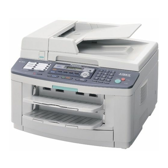
KX-FLB802CX/KX-FLB812CX/KX-FLB802CXS/KX-FLB812CXS 7 Location of Controls and Components 7.1. OVERVIEW 7.1.1. Front view (1) Top cover (2) ADF (Auto Document Feeder) cover release button (3) ADF (Auto Document Feeder) cover (4) Document guides (5) Document tray (6) Document cover (7) Handset... -
Page 71: Control Panel
KX-FLB802CX/KX-FLB812CX/KX-FLB802CXS/KX-FLB812CXS 7.2. CONTROL PANEL (1) Station keys (2) BROADCAST (3) MANUAL BROAD (4) LOWER (5) COLLATE / DIRECTORY (6) CONTRAST (7) RESOLUTION (8) ZOOM/ QUICK SCAN (9) MENU (10) TONE (11) STOP (12) CALLER ID (13) FAX AUTO ANSWER (14) HELP... -
Page 72: Installation Instructions
KX-FLB802CX/KX-FLB812CX/KX-FLB802CXS/KX-FLB812CXS 8 Installation Instructions 8.1. INSTALLATION 8.1.1. INSTALLATION SPACE The space required to install the unit is shown below. The dimensions given are necessary for the unit to operate efficiently. Note: • Avoid excessive heat or humidity. • Use the unit within the following ranges of temperature and humidity. - Page 73 KX-FLB802CX/KX-FLB812CX/KX-FLB802CXS/KX-FLB812CXS 8.1.3.1. For KX-FLB812 users As a default setting, printed paper is stacked on the output tray as follows. - Upper output tray (“#1”): Printed document by using the computer and copied document. - Lower output tray (“#2”): Received fax document.
- Page 74 KX-FLB802CX/KX-FLB812CX/KX-FLB802CXS/KX-FLB812CXS 8.1.3.2. For KX-FLB802 users Pull the output tray extender (1) forward gently until it clicks into place, then press the center part of the extender (2) to open. Note: • The output tray can hold up to approximately 150 sheets of printed paper. Remove the printed paper before the output tray becomes full.
- Page 75 KX-FLB802CX/KX-FLB812CX/KX-FLB802CXS/KX-FLB812CXS If the extender is detached KX-FLB812 Line up the extender (1) underneath the output tray (2), and insert the left side of the extender into the output tray. Attach the extender (1) by bending the side of the output tray down- ward slightly and pressing the right side of the extender.
- Page 76 KX-FLB802CX/KX-FLB812CX/KX-FLB802CXS/KX-FLB812CXS 8.1.4. RECORDING PAPER 8.1.4.1. Using the paper input tray A4, letter or legal size recording paper can be used. The paper input tray unit can hold: — Up to 250 sheets of 60 g/m to 75 g/m (16 lb. to 20 lb.) paper.
- Page 77 KX-FLB802CX/KX-FLB812CX/KX-FLB802CXS/KX-FLB812CXS Load the paper, print-side up (1). Important: • Push and lock the plate (2) in the paper input tray, if it is lifted. • Make sure that the recording paper guides (1) are at the paper size mark and the recording paper is under the paper limit mark (2). The paper should not be over the snubbers.(3)
- Page 78 KX-FLB802CX/KX-FLB812CX/KX-FLB802CXS/KX-FLB812CXS 8.1.4.2. Using the mamual input tray You can print not only on plain paper but also on special media (transparencies / labels / envelopes). The manual input tray is used only for printing with the computer and can hold 1 sheet per time. If multiple pages are needed to be printed, add a next page after the first page is fed into the unit.
- Page 79 KX-FLB802CX/KX-FLB812CX/KX-FLB802CXS/KX-FLB812CXS 8.1.5. HANDSET UNIT Connect the handset cord (1) to the handset and the handset cradle. Connect the handset connecter (1) to the handset unit connection jack (2). Insert the tab (1) into the slot (2) on the unit and insert the rib (3) of the...
- Page 80 KX-FLB802CX/KX-FLB812CX/KX-FLB802CXS/KX-FLB812CXS To remove the handset unit Pull the handset unit slightly forward (1), and then remove the rib of the handset cradle by lifting the handset unit in the direction of the arrow (2). Remove the tab (1) from the slot (2) on the unit and disconnect the...
- Page 81 KX-FLB802CX/KX-FLB812CX/KX-FLB802CXS/KX-FLB812CXS 8.1.6. DOCUMENTS THE UNIT CAN SEND 8.1.6.1. Using the auto document feeder 8.1.6.2. Using the scanner glass Effective scanning area Note for the auto document feeder and the scanner glass • Check that ink, paste or correction fluid has dried completely.
- Page 82 To check the drum life and quality, please print the printer test list. If printing quality is still poor or “Replace Drum” appears on the display , replace the toner cartridge and drum unit. To ensure that the unit operates properly, we recommend the use of Panasonic toner cartridge (Model No.
- Page 83 KX-FLB802CX/KX-FLB812CX/KX-FLB802CXS/KX-FLB812CXS Remove the drum and toner unit (1) by holding the tabs. • If you replace the toner cartridge and the drum unit at the same time, skip to step 7. Turn the two green levers (1) on the used toner cartridge firmly.
- Page 84 KX-FLB802CX/KX-FLB812CX/KX-FLB802CXS/KX-FLB812CXS Firmly press down the toner cartridge to snap into position. Turn the two green levers (1) on the toner cartridge firmly. Make sure that the triangles (1) match to install the toner cartridge cor- rectly. • If the lower glass (2) is dirty, clean it with a soft and dry cloth.
- Page 85 KX-FLB802CX/KX-FLB812CX/KX-FLB802CXS/KX-FLB812CXS • Make sure that the triangles (2) match to install the drum and toner unit correctly. Close the top cover, holding the cover release lever (1) until locked. Caution: • To prevent injuries, be careful not to put your hands under the top cover.
- Page 86 KX-FLB802CX/KX-FLB812CX/KX-FLB802CXS/KX-FLB812CXS 8.1.8. INSTALLING MULTI-FUNCTION STATION • The screenshots shown in these instructions are for Windows XP and are included for reference only. • The screenshots shown in these instructions may differ slightly from those of the actual product. • Software features and appearance are subject to change without notice.
-
Page 87: Connections
8.2.2. Connecting to a computer Panasonic Multi-Function Station software enables the unit to carry out the following functions: - Printing on plain paper, transparencies, labels and envelopes - Scanning documents and converting an image into text with Readiris OCR software - Scanning from other applications for Microsoft®... - Page 88 KX-FLB802CX/KX-FLB812CX/KX-FLB802CXS/KX-FLB812CXS Windows Me: Pentium 150 MHz or faster Windows 2000: Pentium 166 MHz or faster Windows XP*1: Pentium 300 MHz or faster RAM: Windows 98: 24 MB (32 MB or more recommended) Windows Me: 32 MB (64 MB or more recommended)
- Page 89 KX-FLB802CX/KX-FLB812CX/KX-FLB802CXS/KX-FLB812CXS (1) USB cable • Connect to the USB port. Note: • Shielded USB cable (2 m or less in length) must be purchased separately. Be sure to use a USB 2.0 certified cable. • To assure continued emission limit compliance, use only shielded USB cable.
-
Page 90: Operation Instructions
KX-FLB802CX/KX-FLB812CX/KX-FLB802CXS/KX-FLB812CXS 9 Operation Instructions 9.1. YOUR LOGO The logo can be your name or the name of your company. - Page 91 KX-FLB802CX/KX-FLB812CX/KX-FLB802CXS/KX-FLB812CXS 9.1.1. TO SELECT CHARACTERS WITH THE DIAL KEYPAD Pressing the dial keys will select a character as shown below. 9.1.2. TO SELECT CHARACTERS USING [ ] OR [ ]...
-
Page 92: Test Mode
KX-FLB802CX/KX-FLB812CX/KX-FLB802CXS/KX-FLB812CXS 10 Test Mode 10.1. TEST FUNCTIONS The codes listed below can be used to perform simple checks of some of the unit’s functions. When complaints are received from customers, they provide an effective tool for identifying the locations and causes of malfunctions. - Page 93 KX-FLB802CX/KX-FLB812CX/KX-FLB802CXS/KX-FLB812CXS Test Mode Type of Mode Code Function Operation after code input SENSOR CHECK Service Mode “8” “1” “5” First of all, press the copy button, and confirm the action of ON/OFF. For each sensor’s operation, refer to SENSORS AND SWITCHES SECTION (P.49).
- Page 94 KX-FLB802CX/KX-FLB812CX/KX-FLB802CXS/KX-FLB812CXS 10.1.1. DTMF SINGLE TONE TRANSMIT SELECTION Note: After performing this check, do not forget to turn the setting off. otherwise, dialing in DTMF signal will not work. 10.1.2. BUTTON CODE TABLE...
- Page 95 KX-FLB802CX/KX-FLB812CX/KX-FLB802CXS/KX-FLB812CXS 10.1.3. PRINT TEST PATTERN 1. NO.01 3. NO.03 2. NO.06 • These print test patterns are just image printing, and differ- ent from actual ones. • When it is required to judge the print quality, compare with the printing of a nondefective machine.
-
Page 96: Service Mode
KX-FLB802CX/KX-FLB812CX/KX-FLB802CXS/KX-FLB812CXS 11 Service Mode The programming functions are used to program the various features and functions of the machine, and to test the machine. This facilitates communication between the user and the service man while programming the unit. 11.1. PROGRAMMING AND LISTS 11.1.1. - Page 97 KX-FLB802CX/KX-FLB812CX/KX-FLB802CXS/KX-FLB812CXS 11.1.3. SERVICE FUNCTION TABLE Code Function Set Value Effective Default Remarks Range Pause time set X 100 msec 001~600 ---------- Dial speed select 1:10 pps 1, 2 ---------- 2:20 pps V34 transmission start speed 0: Disable 1: 33.6 2: 31.2 3: 28.8...
- Page 98 KX-FLB802CX/KX-FLB812CX/KX-FLB802CXS/KX-FLB812CXS Code Function Set Value Effective Default Remarks Range Time between CED and 300bps 1:75 msec See Symptom/Countermeasure Table for long 2:500 msec distance and international calls in (P.155). Refer to 3:1 sec (P.148) and (P.155). Overseas DIS detection select...
- Page 99 KX-FLB802CX/KX-FLB812CX/KX-FLB802CXS/KX-FLB812CXS 11.1.4. Memory Clear Specification Execute Service Mode #550 when you want to reset the all setting data keeping the user information. Execute Service Mode #710 to clear the user information in case that Main Unit is recycled. Note: Please restart a power supply after clearing a memory.
-
Page 100: User Mode (The List Below Is An Example Of The System Setup List The Unit Prints Out.)
KX-FLB802CX/KX-FLB812CX/KX-FLB802CXS/KX-FLB812CXS 11.2. USER MODE (The list below is an example of the SYSTEM SETUP LIST the unit prints out.) (KX-FLB802) Note: The above values are the default values. - Page 101 KX-FLB802CX/KX-FLB812CX/KX-FLB802CXS/KX-FLB812CXS (KX-FLB812) Note: The above values are the default values.
-
Page 102: Service Mode Settings (Example Of A Printed Out List)
KX-FLB802CX/KX-FLB812CX/KX-FLB802CXS/KX-FLB812CXS 11.3. SERVICE MODE SETTINGS (Example of a printed out list) (KX-FLB802) Note: The above values are the default values. - Page 103 KX-FLB802CX/KX-FLB812CX/KX-FLB802CXS/KX-FLB812CXS (KX-FLB812) Note: The above values are the default values.
-
Page 104: History
KX-FLB802CX/KX-FLB812CX/KX-FLB802CXS/KX-FLB812CXS 11.4. HISTORY Note: See the following descriptions of this report. Item No. (1) ~ (49) are corresponding to the listed items in DESCRIPTIONS OF THE HISTORY REPORT(P.105). - Page 105 KX-FLB802CX/KX-FLB812CX/KX-FLB802CXS/KX-FLB812CXS 11.4.1. DESCRIPTIONS OF THE HISTORY REPORT (1) ROM VERSION (27) NUMBER OF PC-PRINT FLASH ROM version The number of times multifunction was used for the Printer. (2) SUM (The number of pages printed. If the unit does not have a FLASH ROM internal data calculation.
- Page 106 KX-FLB802CX/KX-FLB812CX/KX-FLB802CXS/KX-FLB812CXS (59) NUMBER OF PICK UP ERROR OF RECORDING PAPER TRAY #3 (60) Total number of printing (The number of printed papers including copy, reception printing, report, etc.) (61) The printing number at the most recent maintenance kit replacement (The condition is the same as #60.) (62) The replacement number of the maintenance kit (The number is counted based on the service #670.)
-
Page 107: Troubleshooting Guide
KX-FLB802CX/KX-FLB812CX/KX-FLB802CXS/KX-FLB812CXS 12 Troubleshooting Guide 12.1. USER RECOVERABLE ERRORS If the unit detects a problem, one or more of the following messages will appear on the display. The explanations given in the [ ] are for servicemen only. DISPLAY MESSAGE CAUSE AND REMEDY •... - Page 108 KX-FLB802CX/KX-FLB812CX/KX-FLB802CXS/KX-FLB812CXS DISPLAY MESSAGE CAUSE AND REMEDY • There is something wrong with the unit’s modem. • The other party’s fax machine is busy or has run out of recording paper. Try again. - “#1”: Paper input tray - “#2”: Manual input tray •...
-
Page 109: Remote Programming
KX-FLB802CX/KX-FLB812CX/KX-FLB802CXS/KX-FLB812CXS 12.2. REMOTE PROGRAMMING If, after the call is connected, the customer describes the situation and it is determined that the problem can be corrected by making parameter changes, this function makes it possible to change parameters such as the user code and service code from another fax (using DTMF tones). - Page 110 KX-FLB802CX/KX-FLB812CX/KX-FLB802CXS/KX-FLB812CXS 12.2.1. ENTERING THE REMOTE PROGRAMMING MODE AND CHANGING SERVICE CODES CROSS REFERENCE: PROGRAM MODE TABLE (P.111)
- Page 111 KX-FLB802CX/KX-FLB812CX/KX-FLB802CXS/KX-FLB812CXS 12.2.2. PROGRAM MODE TABLE 12.2.2.1. USER FUNCTION Basic features Code Function Set Value Default Remote Setting SET DATE & TIME mm/dd/yy hh:mm Jan/01/2006 YOUR LOGO --------- None YOUR FAX NUMBER --------- None DIALING MODE 1:Pulse / 2:Tone Tone SET FLASH TIME...
- Page 112 KX-FLB802CX/KX-FLB812CX/KX-FLB802CXS/KX-FLB812CXS 12.2.2.2. SERVICE FUNCTION Code Function Set Value Default Remote Setting Pause time set 001~600 x 100msec Dial speed 1:10pps / 2:20 pps 10pps V34 transmission start speed (0:Disable/1:33.6/2:31.2/3:28.8/4:26.4/ 33600bps 5:24.0/6:21.6/7:19.2/8:16.8/) V34 reception start speed (0:Disable/1:33.6/2:31.2/3:28.8/4:26.4/ 33600bps 5:24.0/6:21.6/7:19.2/8:16.8/) Bell signal detect time...
-
Page 113: Troubleshooting Details
KX-FLB802CX/KX-FLB812CX/KX-FLB802CXS/KX-FLB812CXS NG means “can not set”. Note: Refer to SERVICE FUNCTION TABLE (P.97) for descriptions of the individual codes. Example: If you want to set value in the “401 PRINT CONFIRMATION REPORT”, press the dial key number 1, 2 or 3 corresponding to the Set Value you want to select. - Page 114 KX-FLB802CX/KX-FLB812CX/KX-FLB802CXS/KX-FLB812CXS 12.3.2. STARTING TROUBLE SHOOTING Determine the symptom and the troubleshooting method. CROSS REFERENCE: USER RECOVERABLE ERRORS(P.107) SIMPLE CHECK LIST(P.116) DIGITAL BOARD SECTION(P.253) POWER SUPPLY BOARD SECTION(P.67)
- Page 115 KX-FLB802CX/KX-FLB812CX/KX-FLB802CXS/KX-FLB812CXS 12.3.3. INITIALIZATION There are two types of initialization, one is the short initialization (about 3 seconds) and the other is the long initialization (about 10 seconds). The short initialization makes the unit enter the standby mode. The long initialization makes the unit enter the...
- Page 116 KX-FLB802CX/KX-FLB812CX/KX-FLB802CXS/KX-FLB812CXS 12.3.4. SIMPLE CHECK LIST Note: Check according to the service code referring to TEST FUNCTIONS (P.92)
- Page 117 KX-FLB802CX/KX-FLB812CX/KX-FLB802CXS/KX-FLB812CXS 12.3.5. SIMPLIFIED TROUBLESHOOTING GUIDE 12.3.5.1. PRINTING Symptom Cause Countermeasure GHOST IMAGE (P.128) Failed drum unit Replace drum unit Failed transfer unit Check the transfer roller and spring Failed the high-voltage terminal Check the high-voltage terminal Failed the high voltage power supply board Go to HIGH VOLTAGE SECTION (P.179)
- Page 118 KX-FLB802CX/KX-FLB812CX/KX-FLB802CXS/KX-FLB812CXS 12.3.5.2. RECORDING PAPER FEED Symptom Cause Countermeasure MULTIPLE FEED (P.134) Dirty or failed the pickup roller Clean or replace the pickup roller Dirty or failed the pickup rubber Clean or replace the separation rubber THE RECORDING PAPER Dirty the pressure roller or the heat roller...
- Page 119 KX-FLB802CX/KX-FLB812CX/KX-FLB802CXS/KX-FLB812CXS 12.3.5.3. COPY AND FAX Symptom Cause Countermeasure DOCUMENT FEED Failed the document sensor lever Replace the document sensor lever DOCUMENT Failed the document sensor Go to SENSOR SECTION (P.168) FEED,DOCUMENT Dirty or failed the separation roller Clean or replace the separation roller...
- Page 120 KX-FLB802CX/KX-FLB812CX/KX-FLB802CXS/KX-FLB812CXS 12.3.6. CALL SERVICE TROUBLESHOOTING GUIDE Call Service related error is most frequent. Call Service 1 ----- Polygon doesn’t rotate..Refer to LSU (Laser Scanning Unit) SECTION (P.47). • First, listen to the sound. If rotation sound isn't heard, check 24V line, POLON signal and POLCLK signal. If even a little of sound is heard, check XREADY signal.
- Page 121 KX-FLB802CX/KX-FLB812CX/KX-FLB802CXS/KX-FLB812CXS 12.3.6.1. CALL SERVICE 1 "CALL SERVICE 1" means that the polygon motor inside the LSU does not rotate. The rotation of the polygon motor is detected by IC604-48pin (XREADY).
- Page 122 KX-FLB802CX/KX-FLB812CX/KX-FLB802CXS/KX-FLB812CXS 12.3.6.2. CALL SERVICE 2 "CALL SERVICE 2" means that the synchronous signal out of the LSU cannot be detected. The synchronous signal out of the LSU is detected by IC 604-59pin. (XHSYNC) Note: As for the "Pulse" waveform of the above flow chart, see the timing chart.
- Page 123 KX-FLB802CX/KX-FLB812CX/KX-FLB802CXS/KX-FLB812CXS 12.3.6.3. CALL SERVICE 3 "CALL SERVICE 3" means that the temperature of the fuser does not rise up to or exceed a constant temperature. The temperature is monitored with the thermistor inside the fuser and detected with the voltage input into IC 604-21pin.
- Page 124 KX-FLB802CX/KX-FLB812CX/KX-FLB802CXS/KX-FLB812CXS 12.3.6.4. CALL SERVICE 4 "CALL SERVICE 4" means that the FAN does not run or the running of the FAN cannot be detected normally. The running of the FAN is detected by IC600-16 and 18pin. "CALL SERVICE 4" is displayed when it detects NG three times contin- uously.
- Page 125 KX-FLB802CX/KX-FLB812CX/KX-FLB802CXS/KX-FLB812CXS...
- Page 126 KX-FLB802CX/KX-FLB812CX/KX-FLB802CXS/KX-FLB812CXS 12.3.6.5. CALL SERVICE 5 “CALL SERVICE 5” means that Engine DC motor’s rotation detection signal (LD) does not become Low.
- Page 127 KX-FLB802CX/KX-FLB812CX/KX-FLB802CXS/KX-FLB812CXS 12.3.6.6. CALL SERVICE 6 “CALL SERVICE 6” indicates that abnormal charge voltage is output from the high voltage unit.
- Page 128 KX-FLB802CX/KX-FLB812CX/KX-FLB802CXS/KX-FLB812CXS 12.3.7. PRINT 12.3.7.1. GHOST IMAGE CROSS REFERENCE: HIGH VOLTAGE SECTION(P.179) POWER SUPPLY BOARD SECTION(P.67)
- Page 129 KX-FLB802CX/KX-FLB812CX/KX-FLB802CXS/KX-FLB812CXS 12.3.7.2. DARK OR WHITE VERTICAL LINE Note: When wiping the cover glass, reflecting mirror, use a dry and soft cloth.
- Page 130 KX-FLB802CX/KX-FLB812CX/KX-FLB802CXS/KX-FLB812CXS 12.3.7.3. DARK OR WHITE HORIZONTAL LINE CROSS REFERENCE: HIGH VOLTAGE SECTION (P.179)
- Page 131 KX-FLB802CX/KX-FLB812CX/KX-FLB802CXS/KX-FLB812CXS 12.3.7.4. DIRTY OR HALF DARKNESS BACKGROUND CROSS REFERENCE: HIGH VOLTAGE SECTION (P.179)
- Page 132 KX-FLB802CX/KX-FLB812CX/KX-FLB802CXS/KX-FLB812CXS 12.3.7.5. BLACK PRINT CROSS REFERENCE: HIGH VOLTAGE SECTION (P.179) LSU (Laser Scanning Unit) SECTION (P.47)
- Page 133 KX-FLB802CX/KX-FLB812CX/KX-FLB802CXS/KX-FLB812CXS 12.3.7.6. LIGHT PRINT CROSS REFERENCE: HIGH VOLTAGE SECTION (P.179)
- Page 134 KX-FLB802CX/KX-FLB812CX/KX-FLB802CXS/KX-FLB812CXS 12.3.7.7. BLACK OR WHITE POINT 12.3.8. RECORDING PAPER FEED 12.3.8.1. MULTIPLE FEED...
- Page 135 KX-FLB802CX/KX-FLB812CX/KX-FLB802CXS/KX-FLB812CXS 12.3.8.2. THE RECORDING PAPER IS WAVED OR WRINKLED...
- Page 136 KX-FLB802CX/KX-FLB812CX/KX-FLB802CXS/KX-FLB812CXS 12.3.8.3. SKEW...
- Page 137 KX-FLB802CX/KX-FLB812CX/KX-FLB802CXS/KX-FLB812CXS 12.3.8.4. THE RECORDING PAPER DOES NOT FEED CROSS REFERENCE: SENSOR SECTION (P.168) MOTOR SECTION (P.172)
- Page 138 KX-FLB802CX/KX-FLB812CX/KX-FLB802CXS/KX-FLB812CXS 12.3.8.5. THE RECORDING PAPER JAM...
- Page 139 KX-FLB802CX/KX-FLB812CX/KX-FLB802CXS/KX-FLB812CXS CROSS REFERENCE: FAN MOTOR SECTION (P.44) When the recording paper jam is occurred, the service mode *630 distinguishes the cause. 0:No Paper Jam 1:The paper was pulled into the unit. 2:The paper was longer than the maximum length of the register sensor.
- Page 140 KX-FLB802CX/KX-FLB812CX/KX-FLB802CXS/KX-FLB812CXS 12.3.9. ADF (Auto document feed) SECTION 12.3.9.1. NO DOCUMENT FEED,DOCUMENT JAM and MULTIPLE DOCUMENT FEED. CROSS REFERENCE: SENSOR SECTION (P.168)
- Page 141 KX-FLB802CX/KX-FLB812CX/KX-FLB802CXS/KX-FLB812CXS CROSS REFERENCE: MOTOR SECTION (P.172)
- Page 142 KX-FLB802CX/KX-FLB812CX/KX-FLB802CXS/KX-FLB812CXS 12.3.9.2. SKEW (ADF)
- Page 143 KX-FLB802CX/KX-FLB812CX/KX-FLB802CXS/KX-FLB812CXS 12.3.9.3. THE SENT FAX DATA IS SKEWED CROSS REFERENCE: SKEW (ADF) (P.142) 12.3.9.4. THE RECEIVED FAX DATA IS SKEWED CROSS REFERENCE: SKEW (P.136) 12.3.9.5. THE RECEIVED OR COPIED DATA IS EXPANDED...
- Page 144 KX-FLB802CX/KX-FLB812CX/KX-FLB802CXS/KX-FLB812CXS 12.3.9.6. BLACK OR WHITE VERTICAL LINE IS COPIED...
- Page 145 KX-FLB802CX/KX-FLB812CX/KX-FLB802CXS/KX-FLB812CXS 12.3.9.7. AN ABNORMAL IMAGE IS COPIED CROSS REFERENCE: CIS CONTROL SECTION (P.175) 12.3.10. COMMUNICATION SECTION Find the problem in the table shown below, and refer to the corresponding troubleshooting procedure in DEFECTIVE FACSIM- ILE SECTION (P.146). Symptom Content Possible cause The paper dose not feed properly when faxing.
- Page 146 KX-FLB802CX/KX-FLB812CX/KX-FLB802CXS/KX-FLB812CXS 12.3.10.1. DEFECTIVE FACSIMILE SECTION 12.3.10.1.1. TRANSMIT PROBLEM CROSS REFERENCE: CLEANING THE WHITE PLATE AND GLASSES (P.238) ADF (Auto document feed) SECTION (P.140) OPERATION PANEL SECTION (P.168)
- Page 147 KX-FLB802CX/KX-FLB812CX/KX-FLB802CXS/KX-FLB812CXS 12.3.10.1.2. SOMETIME THERE IS A TRANSMIT PROBLEM Note: “596: Transmit level set” represents a service code. Refer to the SERVICE FUNCTION TABLE (P.97). “717: Transmit speed select” represents a service code. Refer to the SERVICE FUNCTION TABLE (P.97).
- Page 148 KX-FLB802CX/KX-FLB812CX/KX-FLB802CXS/KX-FLB812CXS 12.3.10.1.3. RECEIVE PROBLEM Confirm the following before starting troubleshooting. • Is the recording paper installed properly? Refer to the next page. Note: “596: Transmit level set” represents a service code. Refer to the SERVICE FUNCTION TABLE (P.97). “718: Receive speed select” represents a service code. Refer to the SERVICE FUNCTION TABLE (P.97).
- Page 149 KX-FLB802CX/KX-FLB812CX/KX-FLB802CXS/KX-FLB812CXS 12.3.10.1.4. THE UNIT CAN COPY, BUT CANNOT TRANSMIT/RECEIVE CROSS REFERENCE: TEST FUNCTIONS (P.92)
- Page 150 KX-FLB802CX/KX-FLB812CX/KX-FLB802CXS/KX-FLB812CXS 12.3.11. SPECIAL SERVICE JOURNAL REPORTS Journal 2 and Journal 3 shown below, which are special journals giving the additional detailed information about the latest 35 communications, can be printed by Service Code 881 or 882. Remote printing function for the journal reports (JOURNAL, JOURNAL 2 and JOURNAL 3) is also available for service technicians.
- Page 151 KX-FLB802CX/KX-FLB812CX/KX-FLB802CXS/KX-FLB812CXS 12.3.11.1. JOURNAL 2 Refer to JOURNAL 2 in PRINTOUT EXAMPLE(P.153). Journal 2 displays the additional detailed information about the last 35 communications. Descriptions: (1) RCV. MODE Indicates which receive mode the unit was in when the unit received a fax message.
- Page 152 KX-FLB802CX/KX-FLB812CX/KX-FLB802CXS/KX-FLB812CXS 12.3.11.2. JOURNAL 3 Refer to JOURNAL 3 in PRINTOUT EXAMPLE(P.153). Description (6) ENCODE Compression Code: MH/MR/MMR (7) MSLT MSLT means Minimum Scan Line Time. Used only at the factory. (8) EQM EQM means Eye Quality Monitor. Used only at the factory.
- Page 153 KX-FLB802CX/KX-FLB812CX/KX-FLB802CXS/KX-FLB812CXS 12.3.11.3. PRINTOUT EXAMPLE...
- Page 154 KX-FLB802CX/KX-FLB812CX/KX-FLB802CXS/KX-FLB812CXS...
- Page 155 KX-FLB802CX/KX-FLB812CX/KX-FLB802CXS/KX-FLB812CXS 12.3.11.4. HOW TO OUTPUT THE JOURNAL REPORT 1. Press the MENU button 3 times. 2. Press “#”, then “3”. 3. Press the SET button. 4. The report prints out. CROSS REFERENCE: Features(P.9) Error code table: (1) CODE (2) RESULT...
- Page 156 KX-FLB802CX/KX-FLB812CX/KX-FLB802CXS/KX-FLB812CXS...
- Page 157 KX-FLB802CX/KX-FLB812CX/KX-FLB802CXS/KX-FLB812CXS CROSS REFERENCE: TEST FUNCTIONS (P.92)
- Page 158 KX-FLB802CX/KX-FLB812CX/KX-FLB802CXS/KX-FLB812CXS CROSS REFERENCE: TEST FUNCTIONS (P.92)
- Page 159 KX-FLB802CX/KX-FLB812CX/KX-FLB802CXS/KX-FLB812CXS CROSS REFERENCE: TEST FUNCTIONS (P.92)
- Page 160 KX-FLB802CX/KX-FLB812CX/KX-FLB802CXS/KX-FLB812CXS CROSS REFERENCE: TEST FUNCTIONS (P.92)
- Page 161 KX-FLB802CX/KX-FLB812CX/KX-FLB802CXS/KX-FLB812CXS...
- Page 162 KX-FLB802CX/KX-FLB812CX/KX-FLB802CXS/KX-FLB812CXS...
- Page 163 KX-FLB802CX/KX-FLB812CX/KX-FLB802CXS/KX-FLB812CXS CROSS REFERENCE: TEST FUNCTIONS (P.92)
- Page 164 KX-FLB802CX/KX-FLB812CX/KX-FLB802CXS/KX-FLB812CXS 12.3.12. INITIALIZING ERROR After the power is turned on, the SOC (IC600) initializes and checks each IC. The ROM (IC602), SDRAM (IC601), G/A (IC604) and MODEM (IC607) are checked. If initialization fails for the ICs, the system will not boot up.
- Page 165 KX-FLB802CX/KX-FLB812CX/KX-FLB802CXS/KX-FLB812CXS 12.3.13. ANALOG BOARD SECTION This chapter provides the testing procedures required for the analog parts. A signal route to be tested is determined depending upon purposes. For example, the handset TX route begins at the handset microphone and the signal is output to the telephone line.
- Page 166 KX-FLB802CX/KX-FLB812CX/KX-FLB802CXS/KX-FLB812CXS 12.3.13.2. DEFECTIVE ITS (Integrated Telephone System) SECTION 1. No handset and speakerphone transmission / reception Perform a signal test in the ITS or the NCU section and locate a defective point (where the signal disappears) on each route between the handset microphone and telephone line (sending), or between the telephone line and the handset speaker (receiv- ing), or between the microphone and the telephone line (sending), or between the telephone line and the speaker (receiving).
- Page 167 KX-FLB802CX/KX-FLB812CX/KX-FLB802CXS/KX-FLB812CXS 4. No tone dialing CROSS REFERENCE: CHECK SHEET (P.165) 12.3.13.3. DETECTIVE TAM INTERFACE SECTION 1. The FAX turns on, but does not arrive through TAM. CROSS REFERENCE: TAM INTERFACE SECTION (P.33) 2. A FAX is received, but won't switch from TAM to FAX.
- Page 168 KX-FLB802CX/KX-FLB812CX/KX-FLB802CXS/KX-FLB812CXS 12.3.13.4. OPERATION PANEL SECTION Refer to TEST FUNCTIONS (P.92). 1. NO KEY OPERATION 2. NO LCD INDICATION CROSS REFERENCE: TEST FUNCTIONS (P.92) 12.3.13.5. SENSOR SECTION Refer to SENSORS AND SWITCHES for the circuit description. Perform an SENSOR CHECK to determine if the sensor is operating correctly.
- Page 169 KX-FLB802CX/KX-FLB812CX/KX-FLB802CXS/KX-FLB812CXS 2. Check the paper sensor ..“OUT OF PAPER” INPUT TRAY #1 3. Check the pickup sensor ..“FAILED PICKUP” 4. Check the paper exit sensor ..“PAPER JAMMED” 5. Check the home sensor ..“CARRIAGE ERROR” 6. Check the read position sensor ..“CHECK DOCUMENT”...
- Page 170 KX-FLB802CX/KX-FLB812CX/KX-FLB802CXS/KX-FLB812CXS 7. Check the registration & manual paper sensor ..“PAPER JAMMED” 8. Check the print timing sensor ..“PAPER JAMMED” 9. Check the document sensor 10. Check the ADF cover sensor ..“CLOSE ADF COVER” 11. Check the top cover sensor ..“TOP COVER OPEN”...
- Page 171 KX-FLB802CX/KX-FLB812CX/KX-FLB802CXS/KX-FLB812CXS 12. Check the toner sensor ..“TONER LOW”, “CHANGE DRUM” 13. Check the option handset hook switch CROSS REFERENCE: SENSORS AND SWITCHES SECTION (P.49)
- Page 172 KX-FLB802CX/KX-FLB812CX/KX-FLB802CXS/KX-FLB812CXS 12.3.13.6. MOTOR SECTION 12.3.13.6.1. FB (FlatbedFlatbed) MOTOR...
- Page 173 KX-FLB802CX/KX-FLB812CX/KX-FLB802CXS/KX-FLB812CXS 12.3.13.6.2. ADF MOTOR...
- Page 174 KX-FLB802CX/KX-FLB812CX/KX-FLB802CXS/KX-FLB812CXS 12.3.13.7. LSU SECTION CROSS REFERENCE: LSU (Laser Scanning Unit) SECTION (P.47)
- Page 175 KX-FLB802CX/KX-FLB812CX/KX-FLB802CXS/KX-FLB812CXS 12.3.14. CIS CONTROL SECTION...
- Page 176 KX-FLB802CX/KX-FLB812CX/KX-FLB802CXS/KX-FLB812CXS CROSS REFERENCE: TEST FUNCTIONS (P.92)
- Page 177 KX-FLB802CX/KX-FLB812CX/KX-FLB802CXS/KX-FLB812CXS 12.3.15. HIGH VOLTAGE VALUE CHECK POINT Measurement Procedure 1. Turn Off the unit, and open the unit cover. 2. Remove the developing unit, if it is equipped. 3. Connect the wire to the terminal to be measured (Fig. 2). The wire should be put out of the unit not to interfere in other termi- nals (Fig.
- Page 178 KX-FLB802CX/KX-FLB812CX/KX-FLB802CXS/KX-FLB812CXS...
- Page 179 KX-FLB802CX/KX-FLB812CX/KX-FLB802CXS/KX-FLB812CXS 12.3.16. HIGH VOLTAGE SECTION 1. Main...
- Page 180 KX-FLB802CX/KX-FLB812CX/KX-FLB802CXS/KX-FLB812CXS 2. CHG, GRID...
- Page 181 KX-FLB802CX/KX-FLB812CX/KX-FLB802CXS/KX-FLB812CXS 3. TRA (+)
- Page 182 KX-FLB802CX/KX-FLB812CX/KX-FLB802CXS/KX-FLB812CXS 3. DEV DC...
- Page 183 KX-FLB802CX/KX-FLB812CX/KX-FLB802CXS/KX-FLB812CXS 4. DEV AC...
- Page 184 KX-FLB802CX/KX-FLB812CX/KX-FLB802CXS/KX-FLB812CXS TRA (-)
- Page 185 KX-FLB802CX/KX-FLB812CX/KX-FLB802CXS/KX-FLB812CXS 12.3.17. USB SECTION Troubleshooting 1. Confirmation of the PC settings...
- Page 186 KX-FLB802CX/KX-FLB812CX/KX-FLB802CXS/KX-FLB812CXS 2. Confirmation of the digital unit...
- Page 187 KX-FLB802CX/KX-FLB812CX/KX-FLB802CXS/KX-FLB812CXS USB (Universal Serial Bus) block Description This is a USB block for data communication with PC. Two signal lines (D+/D-) are differential signals which work in reverse phase. VBUS: CN601 1pin D+: CN601 3pin D-: CN601 2pin GND: CN601 4pin...
- Page 188 KX-FLB802CX/KX-FLB812CX/KX-FLB802CXS/KX-FLB812CXS Waveform of normal operation...
- Page 189 KX-FLB802CX/KX-FLB812CX/KX-FLB802CXS/KX-FLB812CXS 12.3.18. POWER SUPPLY BOARD SECTION 12.3.18.1. KEY COMPONENTS FOR TROUBLESHOOTING Check the following parts first: F1, F2, D10-D13, C5, Q1 and PC1. This comes from our experience with experimental test. For example: power supply and lightning surge voltage test, with standing voltage test, intentional short circuit test, etc.
- Page 190 KX-FLB802CX/KX-FLB812CX/KX-FLB802CXS/KX-FLB812CXS 12.3.18.2. TROUBLESHOOTING FLOW CHART...
- Page 191 KX-FLB802CX/KX-FLB812CX/KX-FLB802CXS/KX-FLB812CXS 12.3.18.3. BROKEN PARTS REPAIR DETAILS (D10~D13) Check for a short-circuit in terminal 4. If D10~D13 is short-circuit, F2 will melt (open). In this case, replace all of the parts (D10 - D13, F2). (D101) If D101 is broken, the oscillation circuit in the power supply cannot operate. Check it with an electric tester.
-
Page 192: Document Jams (Auto Document Feeder)
KX-FLB802CX/KX-FLB812CX/KX-FLB802CXS/KX-FLB812CXS 12.4. DOCUMENT JAMS (AUTO DOCUMENT FEEDER) Caution: • Do not pull out the jammed document forcibly before lifting the ADF cover. Hold the ADF cover (1) firmly and lift it to open. When the document has jammed near the document entrance: Remove the jammed document (1) carefully. - Page 193 KX-FLB802CX/KX-FLB812CX/KX-FLB802CXS/KX-FLB812CXS Close the ADF cover.
-
Page 194: Recording Paper Jam
KX-FLB802CX/KX-FLB812CX/KX-FLB802CXS/KX-FLB812CXS 12.5. RECORDING PAPER JAM 12.5.1. When the recording paper has jammed inside of the unit The display will show the following. Caution: • Do not pull out the jammed paper forcibly before opening the top cover. • To prevent injuries, be careful not to put your hands under the top cover. - Page 195 KX-FLB802CX/KX-FLB812CX/KX-FLB802CXS/KX-FLB812CXS Case 1: When the recording paper has jammed near the drum and toner unit: 1. Pull the paper input tray completely out. 2. Remove the jammed paper (1) carefully by pulling it upwards. Remove the jammed paper (1) carefully by pulling it toward you.
- Page 196 KX-FLB802CX/KX-FLB812CX/KX-FLB802CXS/KX-FLB812CXS 3. Push back the green levers (1) to the original position. Case 3: When the recording paper has jammed near the output tray (KX- FLB812CX/KX-FLB812CXS only): 1. Pull and hold the lever (1) to release the jammed paper. 2. Remove the jammed paper (1) carefully by pulling it upwards.
- Page 197 KX-FLB802CX/KX-FLB812CX/KX-FLB802CXS/KX-FLB812CXS 12.5.2. When the recording paper is not fed into the unit properly The display will show the following. Pull the paper input tray completely out, then remove the recording paper and straighten. Re-load the recording paper. insert the paper unit tray into the unit.
- Page 198 KX-FLB802CX/KX-FLB812CX/KX-FLB802CXS/KX-FLB812CXS 12.5.3. When the recording paper in the manual input tray is not fed into the unit properly The display will show the following. Remove the recording paper. Re-insert the recording paper. Note: • If the error message is still displayed, check the recording paper specifications and re-install recording paper.
-
Page 199: Service Fixture & Tools
KX-FLB802CX/KX-FLB812CX/KX-FLB802CXS/KX-FLB812CXS 13 Service Fixture & Tools... -
Page 200: Disassembly And Assembly Instructions
KX-FLB802CX/KX-FLB812CX/KX-FLB802CXS/KX-FLB812CXS 14 Disassembly and Assembly Instructions Note: Remove the Document Cover, the Paper Input tray and the drum and toner cartridge before reassembling. -
Page 201: Lower Cabinet Section
KX-FLB802CX/KX-FLB812CX/KX-FLB802CXS/KX-FLB812CXS 14.1. LOWER CABINET SECTION... -
Page 202: Printer Cover Section
KX-FLB802CX/KX-FLB812CX/KX-FLB802CXS/KX-FLB812CXS 14.2. PRINTER COVER SECTION... -
Page 203: Sorter Section
KX-FLB802CX/KX-FLB812CX/KX-FLB802CXS/KX-FLB812CXS 14.3. SORTER SECTION... -
Page 204: Remove The Both Side Cabinet Section
KX-FLB802CX/KX-FLB812CX/KX-FLB802CXS/KX-FLB812CXS 14.4. REMOVE THE BOTH SIDE CABINET SECTION... -
Page 205: Remove The Left Side Cabinet Section
KX-FLB802CX/KX-FLB812CX/KX-FLB802CXS/KX-FLB812CXS 14.5. REMOVE THE LEFT SIDE CABINET SECTION... -
Page 206: Remove The Bottom Plate
KX-FLB802CX/KX-FLB812CX/KX-FLB802CXS/KX-FLB812CXS 14.6. REMOVE THE BOTTOM PLATE... -
Page 207: Remove The Right Side Cabinet Section
KX-FLB802CX/KX-FLB812CX/KX-FLB802CXS/KX-FLB812CXS 14.7. REMOVE THE RIGHT SIDE CABINET SECTION... -
Page 208: Remove The Alalog Board
KX-FLB802CX/KX-FLB812CX/KX-FLB802CXS/KX-FLB812CXS 14.8. REMOVE THE ALALOG BOARD... -
Page 209: Remove The Digital Board
KX-FLB802CX/KX-FLB812CX/KX-FLB802CXS/KX-FLB812CXS 14.9. REMOVE THE DIGITAL BOARD... -
Page 210: Remove The Mirror
KX-FLB802CX/KX-FLB812CX/KX-FLB802CXS/KX-FLB812CXS 14.10. REMOVE THE MIRROR... -
Page 211: Remove The High Voltage Power Board
KX-FLB802CX/KX-FLB812CX/KX-FLB802CXS/KX-FLB812CXS 14.11. REMOVE THE HIGH VOLTAGE POWER BOARD... -
Page 212: Remove The Laser Unit
KX-FLB802CX/KX-FLB812CX/KX-FLB802CXS/KX-FLB812CXS 14.12. REMOVE THE LASER UNIT... -
Page 213: Remove The Pick Up Roller
KX-FLB802CX/KX-FLB812CX/KX-FLB802CXS/KX-FLB812CXS 14.13. REMOVE THE PICK UP ROLLER... -
Page 214: Remove The Fuser Unit And The Sorter Unit
KX-FLB802CX/KX-FLB812CX/KX-FLB802CXS/KX-FLB812CXS 14.14. REMOVE THE FUSER UNIT AND THE SORTER UNIT... -
Page 215: Remove The Fuser Unit Parts
KX-FLB802CX/KX-FLB812CX/KX-FLB802CXS/KX-FLB812CXS 14.15. REMOVE THE FUSER UNIT PARTS... -
Page 216: Remove The Right Side Cabinet Section
KX-FLB802CX/KX-FLB812CX/KX-FLB802CXS/KX-FLB812CXS 14.16. REMOVE THE RIGHT SIDE CABINET SECTION... -
Page 217: Remove The Operation Panel And Board
KX-FLB802CX/KX-FLB812CX/KX-FLB802CXS/KX-FLB812CXS 14.17. REMOVE THE OPERATION PANEL AND BOARD... -
Page 218: Remove The Scanner Glass Cover
KX-FLB802CX/KX-FLB812CX/KX-FLB802CXS/KX-FLB812CXS 14.18. REMOVE THE SCANNER GLASS COVER... -
Page 219: Remove The Scanner Section
KX-FLB802CX/KX-FLB812CX/KX-FLB802CXS/KX-FLB812CXS 14.19. REMOVE THE SCANNER SECTION... -
Page 220: Remove The Multi Roller
KX-FLB802CX/KX-FLB812CX/KX-FLB802CXS/KX-FLB812CXS 14.20. REMOVE THE MULTI ROLLER... -
Page 221: Remove The Transfer Roller Unit
KX-FLB802CX/KX-FLB812CX/KX-FLB802CXS/KX-FLB812CXS 14.21. REMOVE THE TRANSFER ROLLER UNIT... -
Page 222: Remove The Eject Support Roller Guide Holder
KX-FLB802CX/KX-FLB812CX/KX-FLB802CXS/KX-FLB812CXS 14.22. REMOVE THE EJECT SUPPORT ROLLER GUIDE HOLDER... -
Page 223: Remove The Main Gear Unit
KX-FLB802CX/KX-FLB812CX/KX-FLB802CXS/KX-FLB812CXS 14.23. REMOVE THE MAIN GEAR UNIT... -
Page 224: Remove The Adf Top Cover
KX-FLB802CX/KX-FLB812CX/KX-FLB802CXS/KX-FLB812CXS 14.24. REMOVE THE ADF TOP COVER... - Page 225 KX-FLB802CX/KX-FLB812CX/KX-FLB802CXS/KX-FLB812CXS...
-
Page 226: Remove The Adf Unit
KX-FLB802CX/KX-FLB812CX/KX-FLB802CXS/KX-FLB812CXS 14.25. REMOVE THE ADF UNIT... -
Page 227: Remove The Adf Parts
KX-FLB802CX/KX-FLB812CX/KX-FLB802CXS/KX-FLB812CXS 14.26. REMOVE THE ADF PARTS... -
Page 228: Remove The Sorter Unit Parts
KX-FLB802CX/KX-FLB812CX/KX-FLB802CXS/KX-FLB812CXS 14.27. REMOVE THE SORTER UNIT PARTS... - Page 229 KX-FLB802CX/KX-FLB812CX/KX-FLB802CXS/KX-FLB812CXS...
-
Page 230: Installation Position Of The Lead
KX-FLB802CX/KX-FLB812CX/KX-FLB802CXS/KX-FLB812CXS 14.28. INSTALLATION POSITION OF THE LEAD 14.28.1. LSU SECTION 14.28.2. DIGITAL BOARD SECTION (1) - Page 231 KX-FLB802CX/KX-FLB812CX/KX-FLB802CXS/KX-FLB812CXS 14.28.3. DIGITAL BOARD SECTION (2) 14.28.4. DIGITAL BOARD SECTION (3)
- Page 232 KX-FLB802CX/KX-FLB812CX/KX-FLB802CXS/KX-FLB812CXS 14.28.5. DIGITAL BOARD SECTION (4) 14.28.6. DIGITAL BOARD SECTION (5)
- Page 233 KX-FLB802CX/KX-FLB812CX/KX-FLB802CXS/KX-FLB812CXS 14.28.7. HANDSET SECTION 14.28.8. FAN (RIGHT) MOTOR SECTION...
- Page 234 KX-FLB802CX/KX-FLB812CX/KX-FLB802CXS/KX-FLB812CXS 14.28.9. FAN (LEFT) MOTOR SECTION...
-
Page 235: How To Install Ferrite Core
KX-FLB802CX/KX-FLB812CX/KX-FLB802CXS/KX-FLB812CXS 14.29. HOW TO INSTALL FERRITE CORE... -
Page 236: Maintenace
KX-FLB802CX/KX-FLB812CX/KX-FLB802CXS/KX-FLB812CXS 15 Maintenance 15.1. MAINTENANCE ITEMS AND COMPONENT LOCATIONS 15.1.1. OUTLINE MAINTENANCE AND REPAIRS ARE PERFORMED USING THE FOLLOWING STEPS. 1. Periodic maintenance Inspect the equipment periodically and if necessary, clean any contaminated parts. 2. Check for breakdowns Look for problems and consider how they arose. - Page 237 KX-FLB802CX/KX-FLB812CX/KX-FLB802CXS/KX-FLB812CXS 15.1.2.1. Maintenance List OPERATION CHECK REMARKS Document Path Remove any foreign matter such as paper. — Rollers If the roller is dirty, clean it with a damp cloth then dry thor- Refer to MAINTENANCE CHECK ITEMS/ oughly. COMPONENT LOCATIONS(P.236)
-
Page 238: Maintenance
KX-FLB802CX/KX-FLB812CX/KX-FLB802CXS/KX-FLB812CXS 15.2. MAINTENANCE 15.2.1. CLEANING THE WHITE PLATE AND GLASSES Clean the white plate and glasses when a black line, a white line or a dirty pattern appears on: — your recording paper, — the original document, — the data scanned by the computer, or —... - Page 239 KX-FLB802CX/KX-FLB812CX/KX-FLB802CXS/KX-FLB812CXS Clean the scanner glass (1) and the white cover sheet (2) and its cir- cumference (3) with a soft and dry cloth. • Clean the white cover sheet carefully to avoid damaging it Close the ADF cover (1), then hold the document cover (2) while clean- ing the white plate (3) and the scanner glass(4).
- Page 240 KX-FLB802CX/KX-FLB812CX/KX-FLB802CXS/KX-FLB812CXS If the document cover comes off from the unit Attach the hinges (1) to the document cover (2). • Make sure that the inserted direction is correct. Otherwise, the hinges cannot be inserted into the slots in step 3.
- Page 241 KX-FLB802CX/KX-FLB812CX/KX-FLB802CXS/KX-FLB812CXS 15.2.1.2. Lower glass Disconnect the power cord. Lift the cover release lever (1) and open the top cover (2). Important: • Close the manual input tray (3) before opening the top cover. Note: • Do not touch the transfer roller (5).
- Page 242 KX-FLB802CX/KX-FLB812CX/KX-FLB802CXS/KX-FLB812CXS • Make sure that the triangles (2) match to install the drum and toner unit correctly. Close the top cover, holding the cover release lever (1) until locked. Caution: • To prevent injuries, be careful not to put your hands under the top cover.
- Page 243 KX-FLB802CX/KX-FLB812CX/KX-FLB802CXS/KX-FLB812CXS Clean the document feeder rollers (1) with a cloth moistened with iso- propyl rubbing alcohol, and let all parts dry thoroughly. • Clean the rollers in the direction of the arrow to avoid the discharge brush (2) from being pulled.
-
Page 244: Printing Operation Principle
KX-FLB802CX/KX-FLB812CX/KX-FLB802CXS/KX-FLB812CXS 15.3. PRINTING OPERATION PRINCIPLE 15.3.1. PROCESS CHART AND PROCESS BIAS 15.3.2. CHARGING Charging is the stage that keeps the surface of the sensitive drum a fixed electric potential. The sensitive drum is the Organic Photo Conductor (OPC), which is a electric conductive cylinder whose surface is covered with the Charge Generation Transfer Layer (CGTL). - Page 245 KX-FLB802CX/KX-FLB812CX/KX-FLB802CXS/KX-FLB812CXS 15.3.3. EXPOSING When the drum which is charged with the fixed electric charge is irradiated by the laser beam, the plus charge and minus charge are generated at the Charge Generation Transfer Layer. Passing through the Charge Generation Transfer Layer which conducts the minus charge, the plus-charged drum's surface is neutralized to be skipped.
- Page 246 KX-FLB802CX/KX-FLB812CX/KX-FLB802CXS/KX-FLB812CXS 15.3.5. DEVELOPING AND TRANSCRIPTION The developing is the stage that the OPC drum with an invisible image is changed to visible by the toner. The drum unit consists of mixing paddle, toner supply roller, developing roller, developing blade, charge wire, grid plate and OPC drum. The bias voltage is added to the developing roller and toner supply roller.
- Page 247 KX-FLB802CX/KX-FLB812CX/KX-FLB802CXS/KX-FLB812CXS 15.3.6. CLEANING OF TRANSFER ROLLER The toner attached to the surface of the OPC drum is transferred to the paper at the transcription stage, but a part of the toner remains. The cleaning is the stage that cleans the remain toner after the transcription stage. The remain toner on the drum and the toner which was attached to the place where the laser beam didn't scan are gathered to the developing roller to be used again.
- Page 248 KX-FLB802CX/KX-FLB812CX/KX-FLB802CXS/KX-FLB812CXS 15.3.7. FIXING On the process of the transfer, the transferred toner is weakly attached on the paper. Fixing means the process to fix the toner on the paper permanently. The fixing part melts the toner at the high temperature using the halogen heater. The toner is fixed on the paper by the heat and pressure through the fixing part with the image.
-
Page 249: Transistors And Diodes
KX-FLB802CX/KX-FLB812CX/KX-FLB802CXS/KX-FLB812CXS 15.4. TERMINAL GUIDE OF THE ICs TRANSISTORS AND DIODES 15.4.1. DIGITAL BOARD 15.4.2. ANALOG BOARD... - Page 250 KX-FLB802CX/KX-FLB812CX/KX-FLB802CXS/KX-FLB812CXS 15.4.3. OPERATION BOARD 15.4.4. AFE BOARD 15.4.5. HIGH VOLTAGE POWER SUPPLY BOARD...
- Page 251 KX-FLB802CX/KX-FLB812CX/KX-FLB802CXS/KX-FLB812CXS 15.4.6. LOW VOLTAGE POWER SUPPLY BOARD...
-
Page 252: How To Replace A Flat Package Ic
KX-FLB802CX/KX-FLB812CX/KX-FLB802CXS/KX-FLB812CXS 15.5. HOW TO REPLACE A FLAT PACKAGE IC 15.5.1. PREPARATION • PbF (: Pb free) Solder • Soldering Iron Tip Temperature of 662°F ± 50°F (350°C ± 10°C) Note: We recommend a 30 to 40 Watt soldering iron. An expert may be able to use a 60 to 80 Watt iron where someone with less experience could overheat and damage the PCB foil. -
Page 253: Digital Board Section
KX-FLB802CX/KX-FLB812CX/KX-FLB802CXS/KX-FLB812CXS 15.6. DIGITAL BOARD SECTION When the unit fails to boot up the system, take the troubleshooting procedures very carefully. It may have a serious problem. The symptom: No response when the power is turned on. (No LCD display, and keys are not accepted.) The first step is to check the power source. - Page 254 KX-FLB802CX/KX-FLB812CX/KX-FLB802CXS/KX-FLB812CXS 15.6.1. NG EXAMPLE...
-
Page 255: Test Chart
KX-FLB802CX/KX-FLB812CX/KX-FLB802CXS/KX-FLB812CXS 15.7. TEST CHART 15.7.1. ITU-T No.1 TEST CHART... - Page 256 KX-FLB802CX/KX-FLB812CX/KX-FLB802CXS/KX-FLB812CXS 15.7.2. ITU-T No.2 TEST CHART...
-
Page 257: Schematic Diagram
KX-FLB802CX/KX-FLB812CX/KX-FLB802CXS/KX-FLB812CXS 16 Schematic Diagram 16.1. DIGITAL BOARD (1) +24V TO FAN2 AND +3.3V DRUM SENSOR +3.3V +5VD FAN2HALF CN611 CN602 470 1/2W R628 Q603 FANON R693 Q601 R632 FANDET R634 R630 5.6K 470 1/2W AMP connector FAN2FULL 8.2K 2125 (BLUE) - Page 258 KX-FLB802CX/KX-FLB812CX/KX-FLB802CXS/KX-FLB812CXS +24V XVIDEO 388 s XLDEN R637 XAPC FAN1HALF 8.2K 2125 XHSYNC Q607 [6 ] Q605 +3.3V IC610 +3.3V R638 R815 L668 TO FAN1 TO LASER FAN1FULL 8.2K 2125 R814 Q608 R742 100 R642 FANON 7 GND Q606 39 1/2W R777 5.6K...
-
Page 259: Digital Board (2)
KX-FLB802CX/KX-FLB812CX/KX-FLB802CXS/KX-FLB812CXS 16.2. DIGITAL BOARD (2) -
Page 260: Digital Board (3)
KX-FLB802CX/KX-FLB812CX/KX-FLB802CXS/KX-FLB812CXS 16.3. DIGITAL BOARD (3) +3.3V +3.3V L600 256Mbit SDRAM IC600 IC601 MCLK L705 PVCLK VDD1 VSS54 PRIO[0] SADCLK L706 VSMP DQ15 PRIO[1] SCLK1 DD[0] R844 R836 DD[15] SCLK2 PRIO[2] VDDQ3 SCLK2 VSSQ52 DD[1] R845 R837 DD[14] DEVAC PRIO[3] DQ14... - Page 261 KX-FLB802CX/KX-FLB812CX/KX-FLB802CXS/KX-FLB812CXS +12VCIS +5VD +5VA_C +3.3V L611 TO CIS TRANSIT +5VD Q613 R903 2.2K CN625 R822 R902 1 13VCIS +5VD 0(3216) IC612 2 5V C584 R832 SCLEDR1 C553 6.3V100u 3 VREF AGND2 VINP R901 2 DVDD1 4 SI VRLC/VBIAS SCSI1 5 DG...
-
Page 262: Analog Board
KX-FLB802CX/KX-FLB812CX/KX-FLB802CXS/KX-FLB812CXS 16.4. ANALOG BOARD L281 IC210 L279 C337 R237 C244 C335 K0.027u R378 R377 T200 J206 R257 R375 R273 C266 T201 50V2.2u +24VA R233 R241 Q203 C236 C245 R270 C341 L286 C342 +5VD C262 R383 R382 J100p Q200 L289 R253... - Page 263 KX-FLB802CX/KX-FLB812CX/KX-FLB802CXS/KX-FLB812CXS J223 D209 L262 F200 3A601 L258 C309 +5VD 680p C310 D205 POS200 R343 L266 680p +5VD 3A601 0.5W 6.8 R319 R331 +5VD CN250 +24V 1K2A C320 D216 RLY200 RLY201 RLY200 Q205 D212 C316 R323 J100p Q210 R316 L263 C311 3A601 250V1.0u...
-
Page 264: Tel Jack Board
KX-FLB802CX/KX-FLB812CX/KX-FLB802CXS/KX-FLB812CXS 16.5. TEL JACK BOARD CN206 2 E(G)/A2 a/A1 b/B1 CN251 5 S(W)/B2 a/A1 b/B1 b/B1 R347 a/A1 CN207 R345 S(W) b/B1 R346 a/A1 E(W) KX-FLB802/812CX KX-FLB802/812CXS TEL JACK BOARD 16.6. TONER SENSOR BOARD IC40 OUTPUT CN43 To DIGITAL KX-FLB802/812CX KX-FLB802/812CXS TONER SENSOR BOARD 16.7. -
Page 265: Operation Board
KX-FLB802CX/KX-FLB812CX/KX-FLB802CXS/KX-FLB812CXS 16.9. OPERATION BOARD... -
Page 266: Flatbed Board
KX-FLB802CX/KX-FLB812CX/KX-FLB802CXS/KX-FLB812CXS 16.10. FLATBED BOARD... -
Page 267: Sensor Board
KX-FLB802CX/KX-FLB812CX/KX-FLB802CXS/KX-FLB812CXS 16.11. SENSOR BOARD ADFDOC_A DOCU_LED To ADFRPS PSTART_E DOCU (SENSOR) ADFCVR PSTART To CIS I/F SW 1 PSTART_LED PFLP1719MZ-A DOCUMENT SENSOR BOARD ADFRPS_B DOCU_LED PRINT START SENSOR BOARD PFLP1719MZ- E DOCU To ADFDOC (SENSOR) ADFCVR REGIST_F DOCU_LED REG_LED To ADFMOTOR CABLE... -
Page 268: Handset Board (Option)
KX-FLB802CX/KX-FLB812CX/KX-FLB802CXS/KX-FLB812CXS 16.12. HANDSET BOARD (OPTION) CN941 FLT940 HSMIC+ 2 HSSP+ HOOK_IN 1 HSMIC - HSMIC- 3 HSSP- 4 HSMIC + HSSP+ HSSP- SW940 CN940 KX-FLB802CX/KX-FLB802CXS KX-FLB812CX/KX-FLB812CXS HANDSET BOARD... -
Page 269: High Voltage Power Supply Board
KX-FLB802CX/KX-FLB812CX/KX-FLB802CXS/KX-FLB812CXS 16.13. HIGH VOLTAGE POWER SUPPLY BOARD SW1 F1 +24V 8 56.226KHz TOPCVR CHG REM 8.2K 220K 0.033u 2 11 blue Grid 680K 820K 820K 470p 160K 17.4960KHz DEV AC 6.8K 17.5212KHz 2.2K 100K 680K DEV CLK 100K 220K TRA+/- 60.200KHz... -
Page 270: Low Voltage Power Supply Board
KX-FLB802CX/KX-FLB812CX/KX-FLB802CXS/KX-FLB812CXS 16.14. LOW VOLTAGE POWER SUPPLY BOARD... -
Page 271: Printed Circuit Board
KX-FLB802CX/KX-FLB812CX/KX-FLB802CXS/KX-FLB812CXS 17 Printed Circuit Board 17.1. DIGITAL BOARD DIGITAL BOARD 17.1.1. : COMPONENT VIEW R818 C786 R625 D603 L617 L695 C648 CN601 +12V C650 C584 C658 C649 C710 C651 C582 C583 R626 C904 R817 C782 Q610 R902 C581 D601 R609... - Page 272 KX-FLB802CX/KX-FLB812CX/KX-FLB802CXS/KX-FLB812CXS DIGITAL BOARD 17.1.2. : BOTTOM VIEW C888 R785 C653 C654 R663 C911 C771 C767 R664 C887 R784 R669 C659 R662 FLT603 R726 C647 R619 L612 C568 C643 C795 +24V C644 L721 R624 L614 L705 C642 C932 L709 C907 RESET...
-
Page 273: Analog Board
KX-FLB802CX/KX-FLB812CX/KX-FLB802CXS/KX-FLB812CXS 17.2. ANALOG BOARD ANALOG BOARD 17.2.1. : COMPONENT VIEW J365 J323 CN200 J346 J316 J345 J350 J373 J327 J361 J322 J348 J377 J344 J370 J349 J353 J378 J338 J372 J369 D206 J381 J331 J340 D207 J371 J325 J326 D213... - Page 274 KX-FLB802CX/KX-FLB812CX/KX-FLB802CXS/KX-FLB812CXS ANALOG BOARD 17.2.2. : BOTTOM VIEW L275 J203 L276 L273 L274 J205 L271 J204 R289 R303 C305 R288 R302 L291 L244 R287 R301 R315 C306 R293 R286 R300 C294 C307 C293 C301 R304 R292 R326 R356 L253 C349 R327...
-
Page 275: Tel Jack Board
KX-FLB802CX/KX-FLB812CX/KX-FLB802CXS/KX-FLB812CXS 17.3. TEL JACK BOARD PFUP1521 R345 J382 R347 J383 CN206 CN207 PFUP1521 KX-FLB802/812CX KX-FLB802/812CXS TEL JACK BOARD 17.4. TONER SENSOR BOARD PFUP1521 PFUP1521 PCB-CH AUTO-CH CN43 KX-FLB802/812CX KX-FLB802/812CXS TONER SENSOR BOARD 17.5. HANDSET RELAY BOARD PCB-CH PFUP1521 CN42 PFUP1521... -
Page 276: Operation Board
KX-FLB802CX/KX-FLB812CX/KX-FLB802CXS/KX-FLB812CXS 17.7. OPERATION BOARD OPERATION BOARD 17.7.1. : COMPONENT VIEW J106 J164 J112 J163 J128 J113 J119 J134 J110 C110 J136 J142 C106 J116 J141 J104 J160 J132 J108 J103 J114 J122 J127 J124 J138 J126 J107 J139 J166 C122... - Page 277 KX-FLB802CX/KX-FLB812CX/KX-FLB802CXS/KX-FLB812CXS OPERATION BOARD 17.7.2. : BOTTOM VIEW R131 R128 R133 R132 R105 R130 R129 R106 R113 C103 R110 C116 R119 C107 C108 C114 R114 R120 C115 C113 R121 R123 R125 C112 C104 R122 C111 R127 R103 R115 R116 C109 R124...
-
Page 278: Scanner I/F Board
KX-FLB802CX/KX-FLB812CX/KX-FLB802CXS/KX-FLB812CXS 17.8. SCANNER I/F BOARD 17.8.1. SCANNER I/F BOARD: COMPONENT VIEW FLT52 FLT51 3.15A R62 CN54 SCANNER I/F BOARD COMPONENT VIEW KX-FLB802/812CX KX-FLB802/812CXS... - Page 279 KX-FLB802CX/KX-FLB812CX/KX-FLB802CXS/KX-FLB812CXS 17.8.2. SCANNER I/F BOARD: BOTTOM VIEW SCANNER I/F BOARD BOTTOM VIEW KX-FLB802/812CX KX-FLB802/812CXS...
-
Page 280: Sensor Board
KX-FLB802CX/KX-FLB812CX/KX-FLB802CXS/KX-FLB812CXS 17.9. SENSOR BOARD 17.9.1. DOCUMENT SENSOR BOARD PFUP1524Z -A PFUP1524Z -A KX-FLB802/812CX KX-FLB802/812CXS DOCUMENT SENSOR BOARD 17.9.2. READ POSITION SENSOR BOARD PFUP1524Z -B A PFUP1524Z -B KX-FLB802/812CX KX-FLB802/812CXS READ POSITION SENSOR BOARD 17.9.3. DRUM SENSOR BOARD PFUP1524Z -C PFUP1524Z -C... -
Page 281: Handset Board
KX-FLB802CX/KX-FLB812CX/KX-FLB802CXS/KX-FLB812CXS 17.9.5. PRINT TIMING SENSOR BOARD KX-FLB802/812CX KX-FLB802/812CXS PRINT START SENSOR BOARD 17.9.6. REGISTRATION & MANUAL PAPER SENSOR BOARD PFUP1524Z -F PFUP1524Z -F KX-FLB802/812CX KX-FLB802/812CXS REGISTRATION SENSOR BOARD 17.9.7. THERMISTOR BOARD PFUP1524Z -G PFUP1524Z -G KX-FLB802/812CX KX-FLB802/812CXS THERMISTOR BOARD 17.10. HANDSET BOARD... -
Page 282: High Voltage Power Supply Board
KX-FLB802CX/KX-FLB812CX/KX-FLB802CXS/KX-FLB812CXS 17.11. HIGH VOLTAGE POWER SUPPLY BOARD 17.11.1. COMPONENT VIEW QF530 J5 J6 QF431 D1 D3 (B61) (B1) NQ051 J1 J2 T81 (B81) 0.8A/125V MPH7378 PCPH0415 D85 D84 N0GG4E000004 KX-FBL802CX/KX-FLB802CXS KX-FLB812CX/KX-FLB812CXS : HIGH VOLTAGE POWER SUPPLY BOARD (COMPONENT VIEW) 17.11.2. BOTTOM VIEW... -
Page 283: Low Voltage Power Supply Board
KX-FLB802CX/KX-FLB812CX/KX-FLB802CXS/KX-FLB812CXS 17.12. LOW VOLTAGE POWER SUPPLY BOARD 17.12.1. COMPONENT VIEW T2.5A250V L102 C303 CN101 F301 J107 F501 T2.5A250V L301 D291 C101 T1.6A250V L271 F151 C271 N0AC4GH00001 D104 C501 C151 SCR51 D101 D277 D115 D501 C108 D151 VR101 J105 J104 SEC. -
Page 284: Appendix Information Of Schematic Diagram
KX-FLB802CX/KX-FLB812CX/KX-FLB802CXS/KX-FLB812CXS 18 Appendix Information of Schematic Diagram Note: 1. DC voltage measurements are taken with an oscilloscope or a tester with a ground. 2. The schematic diagrams and circuit board may be modified at any time with the development of new technology. -
Page 285: Exploded View And Replacement Parts List
KX-FLB802CX/KX-FLB812CX/KX-FLB802CXS/KX-FLB812CXS 19 Exploded View and Replacement Parts List 19.1. CABINET, MECHANICAL AND ELECTRICAL PARTS LOCATION 19.1.1. OPERATION PANEL SECTION... - Page 286 KX-FLB802CX/KX-FLB812CX/KX-FLB802CXS/KX-FLB812CXS 19.1.2. RINTER COVER SECTION (1)
- Page 287 KX-FLB802CX/KX-FLB812CX/KX-FLB802CXS/KX-FLB812CXS 19.1.3. ADF SECTION...
- Page 288 KX-FLB802CX/KX-FLB812CX/KX-FLB802CXS/KX-FLB812CXS 19.1.4. PRINT COVER SECTION (2)
- Page 289 KX-FLB802CX/KX-FLB812CX/KX-FLB802CXS/KX-FLB812CXS 19.1.5. PRINTER COVER SECTION (3)
- Page 290 KX-FLB802CX/KX-FLB812CX/KX-FLB802CXS/KX-FLB812CXS 19.1.6. MANUAL TRAY SECTION...
- Page 291 KX-FLB802CX/KX-FLB812CX/KX-FLB802CXS/KX-FLB812CXS 19.1.7. SEPARATION ROLLER SECTION (KX-FLB802only)
- Page 292 KX-FLB802CX/KX-FLB812CX/KX-FLB802CXS/KX-FLB812CXS 19.1.8. UPPER CABINET SECTION...
- Page 293 KX-FLB802CX/KX-FLB812CX/KX-FLB802CXS/KX-FLB812CXS 19.1.9. FUSER SECTION...
- Page 294 KX-FLB802CX/KX-FLB812CX/KX-FLB802CXS/KX-FLB812CXS 19.1.10. MOTOR SECTION...
- Page 295 KX-FLB802CX/KX-FLB812CX/KX-FLB802CXS/KX-FLB812CXS 19.1.11. GEAR SECTION...
- Page 296 KX-FLB802CX/KX-FLB812CX/KX-FLB802CXS/KX-FLB812CXS 19.1.12. LOWER CABINET SECTION (1)
- Page 297 KX-FLB802CX/KX-FLB812CX/KX-FLB802CXS/KX-FLB812CXS 19.1.13. LOWER CABINET SECTION (2)
- Page 298 KX-FLB802CX/KX-FLB812CX/KX-FLB802CXS/KX-FLB812CXS 19.1.14. LOWER CABINET SECTION (3)
- Page 299 KX-FLB802CX/KX-FLB812CX/KX-FLB802CXS/KX-FLB812CXS 19.1.15. MAIN CABINET...
- Page 300 KX-FLB802CX/KX-FLB812CX/KX-FLB802CXS/KX-FLB812CXS 19.1.16. LOWERSIDE CABINET...
- Page 301 KX-FLB802CX/KX-FLB812CX/KX-FLB802CXS/KX-FLB812CXS 19.1.17. CASSETTE DOCUMENT TRAY...
- Page 302 KX-FLB802CX/KX-FLB812CX/KX-FLB802CXS/KX-FLB812CXS 19.1.18. TRAY SECTION 19.1.19. HANDSET CRADLE SECTION...
- Page 303 KX-FLB802CX/KX-FLB812CX/KX-FLB802CXS/KX-FLB812CXS 19.1.20. ACTUAL SIZE OF SCREWS AND WASHER...
- Page 304 KX-FLB802CX/KX-FLB812CX/KX-FLB802CXS/KX-FLB812CXS 19.1.21. ACCESSORIES AND PACKING MATERIALS(KX-FLB802)
- Page 305 KX-FLB802CX/KX-FLB812CX/KX-FLB802CXS/KX-FLB812CXS 19.1.22. ACCESSORIES AND PACKING MATERIALS (KX-FLB812)
-
Page 306: Replacement Parts List
KX-FLB802CX/KX-FLB812CX/KX-FLB802CXS/KX-FLB812CXS 19.2. REPLACEMENT PARTS LIST Ref. Part No. Part Name & Description Remarks RTL (Retention Time Limited) PFBX1250Z1 PUSH BUTTON ABS-HB Notes: PFBX1249Z1 PUSH BUTTON ABS-HB PFBC1143Z2 PUSH BUTTON ABS-HB 1. The marking (RTL) indicates that the Retention Time is... - Page 307 KX-FLB802CX/KX-FLB812CX/KX-FLB802CXS/KX-FLB812CXS Ref. Part No. Part Name & Description Remarks Ref. Part No. Part Name & Description Remarks PFUS1325Z COIL SPRING PF0G1011Z TRANSPARENT PLATE PFDG1455X GEAR POM-HB PFKM1184Z1 CABINET BODY PS-HB PFDR1064Z ROLLER POM-HB PFUS1643Z COIL SPRING PFDF1125Z SHAFT PFDR1066Z ROLLER...
- Page 308 KX-FLB802CX/KX-FLB812CX/KX-FLB802CXS/KX-FLB812CXS Ref. Part No. Part Name & Description Remarks Ref. Part No. Part Name & Description Remarks PFKE1049Z1 GUIDE PS-HB PFDS1015Y ROLLER PFJV1010Z METAL PARTS PFDJ1088Z SPACER PFDR1069Z ROLLER POM-HB PFJT1031Z TERMINAL-TERMINAL PLATE PFUS1568Z BAR SPRING PFMH1085Z METAL PARTS PFUG1033Z...
- Page 309 KX-FLB802CX/KX-FLB812CX/KX-FLB802CXS/KX-FLB812CXS Ref. Part No. Part Name & Description Remarks Ref. Part No. Part Name & Description Remarks PFUS1502Z TORSION SPRING PFDR1067Z PULLEY POM-HB PFJS02N79Z LEAD WIRE,2P PFDE1246Z ANGLE POM-HB PFDN1048Z ROLLER 19.2.1.13. LOWER CABINET SECTION (2) PFDJ1098Z SPACER POM-HB PFUS1610Z...
- Page 310 INSTRUCTION BOOK (IC) PFKS1117Y1 TRAY IC600 C1ZBZ0002831 PFJKFLB851Z MEMORY PARTS IC601 C3ABRG000037 PFQX2364Z INSTRUCTION BOOK IC602 PFWILB802CX1 IC (ROM)(KX-FLB802CX /802CXS) PFQW2403Z INSTRUCTION BOOK IC602 PFWILB812CX1 IC (ROM)(KX-FLB812CX /812CXS) PFJA03A010Z POWER CORD (KX-FLB802CX) IC603 C0CBADD00010 K2CT3EH00005 POWER CORD (KX-FLB802CXS) IC604 C1ZBZ0002767...
- Page 311 KX-FLB802CX/KX-FLB812CX/KX-FLB802CXS/KX-FLB812CXS Ref. Part No. Part Name & Description Remarks Ref. Part No. Part Name & Description Remarks Q639 PQVTD143Z106 TRANSISTOR(SI) C629 ECJ0EF1C104Z Q642 PQVTD143Z106 TRANSISTOR(SI) C630 ECJ0EC1H270J Q644 PQVTD143Z106 TRANSISTOR(SI) C631 ECJ0EF1C104Z D601 PQVDRLS73T DIODE(SI) C632 ECJ0EC1H270J D603 PQVDRLS73T DIODE(SI)
- Page 312 KX-FLB802CX/KX-FLB812CX/KX-FLB802CXS/KX-FLB812CXS Ref. Part No. Part Name & Description Remarks Ref. Part No. Part Name & Description Remarks C709 ECUV1H102KBV 0.001 C783 ECUV1C104ZFV C710 ECUV1H102KBV 0.001 C784 ECUV1C104ZFV C711 ECUV1H102KBV 0.001 C785 ECUV1C104ZFV C712 ECUV1H102KBV 0.001 C786 ECUV1C104ZFV C713 ECUV1H102KBV 0.001...
- Page 313 KX-FLB802CX/KX-FLB812CX/KX-FLB802CXS/KX-FLB812CXS Ref. Part No. Part Name & Description Remarks Ref. Part No. Part Name & Description Remarks C858 ECUV1C104ZFV CN611 K1KA03A00495 CONNECTOR,3P C859 ECUV1C104ZFV CN612 K1KA04A00527 CONNECTOR,4P C860 ECUV1C104ZFV CN613 K1KA07A00257 CONNECTOR,7P C861 ECUV1C104ZFV CN614 K1KA07AA0193 CONNECTOR,7P C862 ECUV1C104ZFV CN615...
- Page 314 KX-FLB802CX/KX-FLB812CX/KX-FLB802CXS/KX-FLB812CXS Ref. Part No. Part Name & Description Remarks Ref. Part No. Part Name & Description Remarks L715 J0JCC0000278 COIL R638 PQ4R10XJ822 8.2k L716 J0JCC0000278 COIL R639 ERJ3GEYJ103 L721 J0JCC0000278 COIL R640 ERJ3GEYJ103 L722 J0JCC0000278 COIL R641 ERJ12YJ471 L723 J0JCC0000278...
- Page 315 KX-FLB802CX/KX-FLB812CX/KX-FLB802CXS/KX-FLB812CXS Ref. Part No. Part Name & Description Remarks Ref. Part No. Part Name & Description Remarks R742 ERJ3GEYJ101 R846 ERJ2GEJ470 R743 ERJ3GEYJ101 R847 ERJ2GEJ470 R744 ERJ3GEYJ101 R848 ERJ2GEJ470 R745 ERJ3GEYJ473 R849 ERJ2GEJ470 R746 ERJ3GEYJ472 4.7k R850 ERJ2GEJ470 R747 ERJ6GEY0R00...
- Page 316 KX-FLB802CX/KX-FLB812CX/KX-FLB802CXS/KX-FLB812CXS Ref. Part No. Part Name & Description Remarks Ref. Part No. Part Name & Description Remarks (TRANSISTORS) C305 ECUV1H820JCV Q200 B1AAKL000006 TRANSISTOR(SI) C306 ECUV1H820JCV Q203 2SB1218ARL TRANSISTOR(SI) C307 ECUV1H820JCV Q204 PQVTDTC143E TRANSISTOR(SI) C308 ECJ1VC1H680J Q206 B1CCBR000001 TRANSISTOR(SI) C309 ECKD2H681KB...
- Page 317 KX-FLB802CX/KX-FLB812CX/KX-FLB802CXS/KX-FLB812CXS Ref. Part No. Part Name & Description Remarks Ref. Part No. Part Name & Description Remarks PC200 0N3131SKU PHOTO COUPLER R328 ERJ3GEYJ820 PC201 0N3131SKU PHOTO COUPLER R329 ERJ3GEYJ102 PC203 B3PAB0000058 PHOTO COUPLER R332 ERDS1TJ682 6.8k R333 ERJ3GEYJ471 PC205 B3PAA0000425...
- Page 318 KX-FLB802CX/KX-FLB812CX/KX-FLB802CXS/KX-FLB812CXS Ref. Part No. Part Name & Description Remarks Ref. Part No. Part Name & Description Remarks ECUV1C104ZFV R112 ERJ3GEYJ181 R113 ERJ3GEYJ241 19.2.8. HANDSET RELAY BOARD PARTS R114 ERJ3GEYJ241 R119 ERJ3GEYJ4R7 R121 ERJ3GEYJ561 Ref. Part No. Part Name & Description...
- Page 319 KX-FLB802CX/KX-FLB812CX/KX-FLB802CXS/KX-FLB812CXS 19.2.11. SCANNER BOARD PARTS Ref. Part No. Part Name & Description Remarks ERJ3GEYJ2R2 ERJ12RQG1R0 Ref. Part No. Part Name & Description Remarks ERJ3GEYJ472 4.7k ERJ12RQG1R0 PCB8 PFLP1718MZ SCANNER I/F BOARD ASS'Y (RTL) ERJ3GEYJ102 (IC's) ERJ3GEYJ102 IC51 C0GBF0000026 ERJ3GEYJ104 100k...
- Page 320 KX-FLB802CX/KX-FLB812CX/KX-FLB802CXS/KX-FLB812CXS 19.2.16. PRINT START SENSOR BOARD Ref. Part No. Part Name & Description Remarks PARTS PFVDRD150S DIODE(SI) PFVDRD150S DIODE(SI) PFVDMTZJ39A DIODE(SI) Ref. Part No. Part Name & Description Remarks PFVDMTZJ7R5A DIODE(SI) PFVDMTZJ39A DIODE(SI) PCB13 PFLP1719MZ-E PRINT START SENSOR BOARD PFVDRD150S...
- Page 321 KX-FLB802CX/KX-FLB812CX/KX-FLB802CXS/KX-FLB812CXS Ref. Part No. Part Name & Description Remarks Ref. Part No. Part Name & Description Remarks ERJ3GEYF333 PSVDERA1506 DIODE(SI) ERJ3GEYJ563 D101 PFVDYG911S2 DIODE(SI) ERJ3GEYJ222 2.2k D104 PFVDTZPT8130 DIODE(SI) ERJ3GEYJ225 2.2M PSVDERA1506 DIODE(SI) ERJ3GEYJ225 2.2M D110 PFVDHZS7L DIODE(SI) ERJ3GEYJ225 2.2M...
- Page 322 KX-FLB802CX/KX-FLB812CX/KX-FLB802CXS/KX-FLB812CXS 19.2.21. HOOK SWITCH BOARD Ref. Part No. Part Name & Description Remarks R105 PQ4R10XJ103 R106 ERJ3GEYJ123 Ref. Part No. Part Name & Description Remarks PQ4R10XJ912 9.1k R115 PQ4R18XJ4R7 PCB18 PFLP1696MZ HOOK SWITCH BOARD (RTL) ERJ3GEYJ223 (JACKS) ERJ3GEYJ331 CN940 PQJJ1TC5Z...
- Page 323 KX-FLB802CX/KX-FLB812CX/KX-FLB802CXS/KX-FLB812CXS YF(Q) KXFLB802/KXFLB812...