Sony CDP-XE220 Service Manual
Hide thumbs
Also See for CDP-XE220:
- Operating instructions manual (56 pages) ,
- Operating instructions manual (56 pages) ,
- Service manual (21 pages)
Table of Contents
Advertisement
QQ
3 7 63 1515 0
SERVICE MANUAL
Ver 1.1 2001. 05
TE
L 13942296513
www
.
9-922-805-12
Son y Corporation
Home Audio Company
2001E0200-1
Shinagawa Tec Service Manual Production Group
© 2001.5
http://www.xiaoyu163.com
CDP-XE220/XE320
x
ao
y
i
http://www.xiaoyu163.com
8
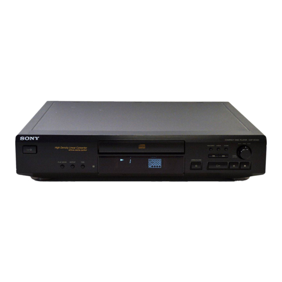
Photo: CDP-XE320
Model Name Using Similar Mechanism
CD Mechanism Type
Base Unit Type
Optical Pick-up Type
Q Q
SPECIFICATIONS
3
6 7
1 3
u163
.
– 1 –
2 9
9 4
2 8
AEP Model
CDP-XE210/XE310
CDM14FL-5BD29C
BU-5BD29C
KSS-213BA/F-NP
1 5
0 5
8
2 9
9 4
m
COMPACT DISC PLAYER
co
9 9
UK Model
2 8
9 9
Advertisement
Table of Contents

Related Manuals for Sony CDP-XE220


Summary of Contents for Sony CDP-XE220
- Page 1 CDP-XE220/XE320 3 7 63 1515 0 SERVICE MANUAL AEP Model UK Model Ver 1.1 2001. 05 Photo: CDP-XE320 Model Name Using Similar Mechanism CDP-XE210/XE310 CD Mechanism Type CDM14FL-5BD29C Base Unit Type BU-5BD29C Optical Pick-up Type KSS-213BA/F-NP SPECIFICATIONS L 13942296513...
-
Page 2: Table Of Contents
WITH MARK ! ON THE SCHEMATIC DIAGRAMS AND IN THE PARTS LIST ARE CRITICAL TO SAFE OPERATION. REPLACE THESE COMPONENTS WITH SONY PARTS WHOSE PART NUMBERS APPEAR AS SHOWN IN THIS MANUAL OR IN SUPPLEMENTS PUBLISHED BY SONY. – 2 – http://www.xiaoyu163.com... -
Page 3: Servicing Note
http://www.xiaoyu163.com SECTION 1 SERVICING NOTE 3 7 63 1515 0 HOW TO OPEN THE DISC TRAY WHEN POWER SWITCH NOTES ON HANDLING THE OPTICAL PICK-UP BLOCK TURNS OFF OR BASE UNIT Insert a tapering driver into the aperture of the unit bottom, and turn The laser diode in the optical pick-up block may suffer in the direction of arrow. -
Page 4: General
http://www.xiaoyu163.com SECTION 2 3 7 63 1515 0 GENERAL Front Panel 3 4 5 LOCATION OF PARTS AND CONTROLS 1 1/u switch 2 DISC tray 3 PEAK SEARCH button 4 CHECK button 5 CLEAR button L 13942296513 6 0,) button 7 ≠, AMS * ±... -
Page 5: Disassembly
http://www.xiaoyu163.com SECTION 3 DISASSEMBLY 3 7 63 1515 0 Note : Follow the disassembly procedure in the numerical order given. 3-1. FRONT PANEL • In order to remove the front panel block when the power supply does not turn on, rotate the cam with tapering driver as the figure shows, and the loading part will be moved. -
Page 6: Test Mode
http://www.xiaoyu163.com SECTION 4 TEST MODE 3 7 63 1515 0 4-2. ADJ MODE 4-1. AF MODE The following operations are performed in the ADJ mode, which The following checks can be performed in the AF mode, which is is set by connecting the TP3 (JW41 : ADJ) terminal to the Ground set by connecting the TP2 (JW40 : AFADJ) terminal on MAIN board and turning on the power. - Page 7 http://www.xiaoyu163.com 3 7 63 1515 0 [ MAIN BOARD ] — Component Side — IC401 (JW41: ADJ) (JW40: AF ADJ) CN402 L 13942296513 u163 – 7 – http://www.xiaoyu163.com...
-
Page 8: Electrical Block Checking
http://www.xiaoyu163.com SECTION 5 ELECTRICAL BLOCK CHECKING 3 7 63 1515 0 Note: Note: 1. CD Block is basically designed to operate without adjustment. A clear RF signal waveform means that the shape “◊” can be clearly Therefore, check each item in order given. distinguished at the center of the waveform. -
Page 9: Diagrams
http://www.xiaoyu163.com SECTION 6 DIAGRAMS 3 7 6 3 1 5 1 5 0 6. Check the level B of the oscilliscope's waveform and the A (DC Adjustment Location : 6-1. CIRCUIT BOARDS LOCATION BD board voltage) of the center of the Traverse waveform. Confirm the following : [ BD BOARD ] —... -
Page 10: Printed Wiring Board - Cd Section
CDP-XE220/XE320 3 7 6 3 1 5 1 5 0 6-2. PRINTED WIRING BOARD – CD SECTION – • See page 10 for Circuit Boards Location. • Semiconductor Location Ref. No. Location IC101 IC102 IC103 Q101 1 3 9 4 2 2 9 6 5 1 3 (Page 15) •... -
Page 11: Schematic Diagram - Cd Section
CDP-XE220/XE320 3 7 6 3 1 5 1 5 0 6-3. SCHEMATIC DIAGRAM – CD SECTION – • See page 10 for Waveforms. • See page 23 for IC Pin Functions. • See page 29 for IC Block Diagrams. -
Page 12: Printed Wiring Board - Main Section
CDP-XE220/XE320 3 7 6 3 1 5 1 5 0 6-4. PRINTED WIRING BOARD – MAIN SECTION – • See page 10 for Circuit Boards Location. • Semiconductor Location Ref. No. Location D401 D402 D403 D404 D701 D702 D703... -
Page 13: Schematic Diagram - Main Section
CDP-XE220/XE320 3 7 6 3 1 5 1 5 0 6-5. SCHEMATIC DIAGRAM – MAIN SECTION – • See page 31 for IC Block Diagrams. 1 3 9 4 2 2 9 6 5 1 3 (Page 21) w w w... -
Page 14: Printed Wiring Board - Panel Section
CDP-XE220/XE320 3 7 6 3 1 5 1 5 0 6-6. PRINTED WIRING BOARD – PANEL SECTION – • See page 10 for Circuit Boards Location. (Page 15) 1 3 9 4 2 2 9 6 5 1 3... -
Page 15: Schematic Diagram - Panel Section
CDP-XE220/XE320 3 7 6 3 1 5 1 5 0 6-7. SCHEMATIC DIAGRAM – PANEL SECTION – • See page 10 for Waveforms. • See page 28 for IC Pin Functions. 1 3 9 4 2 2 9 6 5 1 3... -
Page 16: Ic Pin Functions
http://www.xiaoyu163.com 3 7 6 3 1 5 1 5 0 6-8. IC PIN FUNCTIONS Pin No. Pin Name Function • IC101 FOCUS/TRACKING/SLED SERVO RF AMP (CXA1992AR) RF summing amplifier inverted input RF M The RF amplifier gain is determined by the resistance connected between this pin and Pin No. - Page 17 http://www.xiaoyu163.com 3 7 63 1515 0 • IC103 DIGITAL SIGNAL PROCESSOR (CXD2529Q) Pin Name Function Pin No. – +5V power supply – Ground Lch “L” detection flog LMUT Rch “L” detection flog RMUT Test output (Not used) ACDT Master clock divider output (Not used) CKOUT Clock input for SQSO read out SQCK...
- Page 18 http://www.xiaoyu163.com 3 7 63 1515 0 Pin Name Function Pin No. AVSS Analog ground – CLTV Control voltage input for VCO AVDD Analog power supply – EFM signal input Asymmetry circuit constant current input BIAS ASYI Asymmetry comparate voltage input EFM full swing output (“L”...
- Page 19 http://www.xiaoyu163.com 3 7 63 1515 0 Pin Name Function Pin No. — Not used – AVSS – Analog ground AVDD Analog power supply – AOUT1 Lch analog output AIN1 Lch opamp input LOUT1 Lch line output AVSS Analog ground – XVDD Master clock power supply –...
- Page 20 http://www.xiaoyu163.com 3 7 63 1515 0 • IC501 SYSTEM CONTROL ( CXP82616-034Q) Pin No. Pin Name Function – Ground RMIN Remote control signal input – Ground 4 to 7 — – Not used Serial clock output SENSE Sense signal input from IC103 (CXD2529Q) DATA Serial data output SQCK...
-
Page 21: Ic Block Diagrams
http://www.xiaoyu163.com 3 7 63 1515 0 6-9. IC BLOCK DIAGRAMS • CD section IC101 CXA1992AR – RF SUMMING PD2 IV PD1 IV FE_BIAS SENS2 ↓ – SENS1 LASER POWER CONTROL F IV AMP FE AMP – C. OUT E IV AMP –... - Page 22 http://www.xiaoyu163.com 3 7 63 1515 0 IC102 BA5941FP – + – + – LEVEL SHIFT LEVEL SHIFT LEVEL SHIFT – LEVEL SHIFT – – + – – + – MUTE L 13942296513 IC103 CXD2529Q 80 79 78 77 76 75 74 73 72 71 70 69 68 67 66 65 64 63 62 61 60 59 58 57 56 55 54 53 52 51 LRCK AVSS...
- Page 23 http://www.xiaoyu163.com 3 7 63 1515 0 • MAIN section IC401 LB1641 DRIVER INPUT LOGIC BLOCK OUT1 OUT2 L 13942296513 IC701 LA5601 V REF VOMUTE RESET ON/OFF u163 – 31 – http://www.xiaoyu163.com...
-
Page 24: Exploded Views
4-996-562-51 PANEL, LOADING…(SILVER) (XE220) * 14 4-978-901-21 CASE (408226)…(BLACK) 4-996-687-21 KNOB (AMS) * 14 4-980-193-41 CASE (408226)…(SILVER) (XE220) 4-996-698-21 EMBLEM, SONY ! 15 1-575-651-21 CORD, POWER 4-996-560-01 WINDOW (FL) X-4947-207-1 FOOT ASSY (F50150S) 4-977-593-01 RING (DIA. 50), ORNAMENTAL * 17 4-954-051-51 HOLDER, PC BOARD X-4949-358-1 PANEL ASSY, FRONT…(BLACK) (XE220) -
Page 25: Cd Mechanism Section (Cdm14Fl-5Bd29C)
http://www.xiaoyu163.com 3 7 63 1515 0 7-2. CD MECHANISM SECTION (CDM14FL-5BD29C) NOTE: There are two types of MAGNET ASSY. Confirm the shape before replacing the parts. BU-5BD29C not supplied not supplied not supplied L 13942296513 M151 Ref. No. Part No. Description Remark Ref. -
Page 26: Base Unit Section (Bu-5Bd29C)
http://www.xiaoyu163.com 3 7 63 1515 0 7-3. BASE UNIT SECTION (BU-5BD29C) L 13942296513 M102 M101 The components identified by mark ! or dotted line with mark ! are critical for safety. Replace only with part number specified. Ref. No. Part No. Description Remark Ref. - Page 27 http://www.xiaoyu163.com SECTION 8 ELECTRICAL PARTS LIST 3 7 63 1515 0 Note: • Due to standardization, replacements in the parts list • SEMICONDUCTORS The components identified by mark ! may be different from the parts specified in the In each case, u: µ , for example: or dotted line with mark ! are critical diagrams or the components used on the set.
- Page 28 http://www.xiaoyu163.com LOADING MAIN 3 7 63 1515 0 Ref. No. Part No. Description Remark Ref. No. Part No. Description Remark R120 1-216-089-91 RES, CHIP 1/10W 1-645-721-11 LOADING BOARD R121 1-216-114-00 RES, CHIP 510K 1/10W ************** R122 1-216-097-91 RES, CHIP 100K 1/10W <...
- Page 29 http://www.xiaoyu163.com PANEL MAIN 3 7 63 1515 0 Ref. No. Part No. Description Remark Ref. No. Part No. Description Remark C905 1-161-494-00 CERAMIC 0.022uF R308 1-247-891-00 CARBON 330K 1/4W R310 1-247-807-31 CARBON 1/4W < CONNECTOR > R311 1-249-429-11 CARBON 1/4W R312 1-249-429-11 CARBON 1/4W...
- Page 30 CDP-XE220/XE320 PANEL POWER SW 3 7 63 1515 0 Ref. No. Part No. Description Remark Ref. No. Part No. Description Remark < CONNECTOR > 1-668-618-11 POWER SW BOARD **************** * CN501 1-568-864-11 SOCKET, CONNECTOR 21P < SWITCH > < FLUORESCENT INDICATOR >...
- Page 31 CDP-XE220/XE320 3 7 63 1515 0 – MEMO – L 13942296513 u163 – 39 – http://www.xiaoyu163.com...
- Page 32 Clicking the version allows you to jump to the revised page. Also, clicking the version at the upper right on the revised page allows you to jump to the next revised page. Ver. Date Description of Revision 2001.05 Silver model added for CDP-XE220. (SFD-01006) 1998.04 L 13942296513 u163 http://www.xiaoyu163.com...