Sony CDP-XE270 Service Manual
Compact disc player
Hide thumbs
Also See for CDP-XE270:
- Specifications (1 page) ,
- Operating instructions manual (36 pages) ,
- Limited warranty (1 page)
Table of Contents
Advertisement
SERVICE MANUAL
Ver. 1.4 2006.07
Compact disc player
Laser
Frequency response
Dynamic range
Harmonic distortion
Outputs
ANALOG
OUT
DIGITAL
OUT
(OPTICAL)
Sony Corporation
9-929-591-15
2006G05-1
Home Audio Division
© 2006.07
Published by Sony Techno Create Corporation
CDP-XE270/XE370
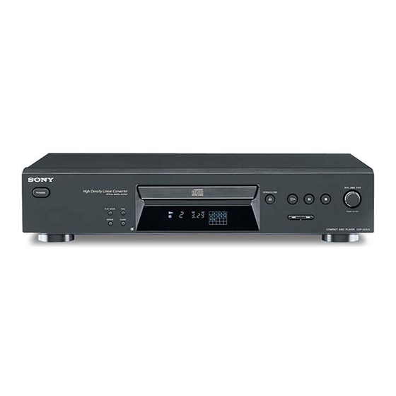
Photo: CDP-XE370
SPECIFICATIONS
Semiconductor laser (λ =
780 nm)
Emission duration:
continuous
2 Hz to 20 kHz ± 0.5 dB
More than 93 dB
0.0045%
Jack
Maximum
Load
type
output level
impedance
Phono
2 V
Over 10
jacks
(at 50
kilohms
kilohms)
Optical
–18 dBm
Wave length:
output
660 nm
connector
Model Name Using Similar Mechanism
CD Mechanism Type
Base Unit Name
Optical Pick-up Name
General
Power requirements
Power requirements
Where purchased
120 V AC, 60 Hz
US, Canadian models
AEP, UK models
230 V AC, 50/60 Hz
Australian model
240 V AC, 50/60 Hz
Singapore model
220 V– 230 V AC, 50/60 Hz
Power consumption
11 W
Dimensions (approx.)
430 x 95 x 290 mm
(w/h/d)
incl. projecting parts
Mass (approx.)
CDP-XE370: 3.2 kg
CDP-XE270: 3.2 kg
Supplied accessories
Audio cord (2 phono plugs – 2 phono plugs) (1)
Remote commander (remote) (1) (CDP-XE370 only)
R6 (size AA) batteries (2) (CDP-XE370 only)
Design and specifications are subject to change
without notice.
COMPACT DISC PLAYER
US Model
AEP Model
UK Model
E Model
Australian Model
CDP-XE270/XE370
Canadian Model
CDP-XE270
NEW
CDM66-5BD27
BU-5BD27
PXR-104X or KSS-213C
Advertisement
Table of Contents

Related Manuals for Sony CDP-XE270


Summary of Contents for Sony CDP-XE270
- Page 1 Remote commander (remote) (1) (CDP-XE370 only) (OPTICAL) connector R6 (size AA) batteries (2) (CDP-XE370 only) Design and specifications are subject to change without notice. COMPACT DISC PLAYER Sony Corporation 9-929-591-15 2006G05-1 Home Audio Division © 2006.07 Published by Sony Techno Create Corporation...
-
Page 2: Table Of Contents
CDP-XE270/XE370 Ver 1.1 2001.07 TABLE OF CONTENTS SERVICING NOTES ..........4 GENERAL ..............5 DISASSEMBLY 3-1. Disassembly Flow ............6 3-2. Case ................. 6 3-3. CD Mechanism Deck (CDM66-5BD27) ......7 3-4. MAIN Board ..............7 3-5. Base Unit (BU-5BD27) ........... 8 TEST MODE .............. - Page 3 OPERATION. REPLACE THESE COMPONENTS WITH DE FONCTIONNEMENT. NE REMPLACER CES COM- SONY PARTS WHOSE PART NUMBERS APPEAR AS POSANTS QUE PAR DES PIÈCES SONY DONT LES SHOWN IN THIS MANUAL OR IN SUPPLEMENTS PUB- NUMÉROS SONT DONNÉS DANS CE MANUEL OU LISHED BY SONY.
-
Page 4: Servicing Notes
CDP-XE270: UK model 4-232-151-1 on the disc reflective surface by the objective lens in the optical CDP-XE270: US and Canadian models 4-232-151-2 pick-up block. Therefore, when checking the laser diode emis- sion, observe from more than 30 cm away from the objective lens. -
Page 5: General
CDP-XE270/XE370 SECTION 2 This section is extracted from instruction manual. GENERAL LOCATION OF CONTROLS – REMOTE CONTROL – – FRONT PANEL – (CDP-XE370 only) CLEAR qg (12) BUTTON DESCRIPTIONS Disc compartment 6 (8) A OPEN/CLOSE 7 (8, 10, 12) Display qj (10) -
Page 6: Disassembly
CDP-XE270/XE370 SECTION 3 DISASSEMBLY • This set can be disassembled in the order shown below. 3-1. DISASSEMBLY FLOW 3-2. CASE (Page 6) 3-3. CD MECHANISM DECK 3-4. MAIN BOARD (CDM66-5BD27) (Page 7) (Page 7) 3-5. BASE UNIT (BU-5BD27) (Page 8) Note: Follow the disassembly procedure in the numerical order given. -
Page 7: Cd Mechanism Deck (Cdm66-5Bd27)
CDP-XE270/XE370 3-3. CD MECHANISM DECK (CDM66-5BD27) 5 three screws (BVTP3 7 connector (CN151) 8 CD mechanism deck (CDM66-5BD27) 4 wire (flat type) (21core) – BOTTOM VIEW – 1 tapering driver 3 panel, loading Note: When the power supply does not turn on, rotate the cam with tepering driver ( 3 mm) as the figure shows, and the loading panel will be moved. -
Page 8: Base Unit (Bu-5Bd27)
CDP-XE270/XE370 3-5. BASE UNIT (BU-5BD27) – BOTTOM VIEW – 6 base unit (BU-5BD27) 3 three screws (DIA. 12), froating 5 two springs (932), compression 5 two springs (932), compression 4 holder (66) 1 screw (DIA. 12), froating... -
Page 9: Test Mode
CDP-XE270/XE370 SECTION 4 TEST MODE AGING MODE AFADJ MODE (KEY AND FLUORESCENT INDICA- Procedure: TOR TUBE DISPLAY CHECK MODE) [CLEAR] 1. While pressing the both buttons, turn the Procedure: power on. 1. Short-circuit the test TP (AFADJ) of the DISPLAY board and 2. - Page 10 CDP-XE270/XE370 Checking Location: – DISPLAY BOARD (Conductor Side) – (GND) (AFADJ) (ADJ)
-
Page 11: Electrical Checks
CDP-XE270/XE370 Ver 1.1 2001.07 SECTION 5 ELECTRICAL CHECKS Procedure: Note: 1. CD Block is basically designed to operate without adjustment. There- Connect an oscilloscope to test point TP (RFDC) and TP (VC) fore, check each item in order given. on the BD board. - Page 12 CDP-XE270/XE370 Ver 1.1 2001.07 E-F Balance Check Checking Location: Connection: – BD BOARD (Conductor Side) – oscilloscope BD board TP (TE1) TP (VC) – Procedure: Connect an oscilloscpe to test point TP (TE1) and TP (VC) on the BD board.
-
Page 13: Diagrams
CDP-XE270/XE370 SECTION 6 DIAGRAMS 6-1. NOTE FOR PRINTED WIRING BOARDS AND SCHEMATIC DIAGRAMS • Circuit Boards Location Note on Printed Wiring Board: Note on Schematic Diagram: • X : parts extracted from the component side. • All capacitors are in µF unless otherwise noted. pF: µµF •... -
Page 14: Printed Wiring Board - Bd Board
CDP-XE270/XE370 Ver 1.1 2001.07 6-2. PRINTED WIRING BOARD – BD Board – • See page 13 for Circuit Boards Location. M101 BD BOARD (SPINDLE) BD BOARD (COMPONENT SIDE) (CONDUCTOR SIDE) TP (DGND) S101 (LIMIT) C154 C158 C151 C152 R152 R155... -
Page 15: Schematic Diagram - Bd Board
CDP-XE270/XE370 Ver 1.1 2001.07 6-3. SCHEMATIC DIAGRAM – BD Board – • See page 20 for Waveforms. • See page 20 for IC Block Diagrams. (RFDC) (Page 17) -
Page 16: Printed Wiring Boards
CDP-XE270/XE370 6-4. PRINTED WIRING BOARDS – LOADING/MAIN/POWER SW Boards – • See page 13 for Circuit Boards Location. • Semiconductor Location Ref. No. Location MAIN BOARD D601 D602 JW666 D603 D604 D605 D612 R682 IC651 D613 DIGITAL D614 JW683 OPTICAL... -
Page 17: Schematic Diagram - Loading/Main/Power Sw Boards
CDP-XE270/XE370 6-5. SCHEMATIC DIAGRAM – LOADING/MAIN/POWER SW Boards – • See page 20 for IC Block Diagram. (Page 15) (Page 19) -
Page 18: Printed Wiring Boards - Display/Key Boards
CDP-XE270/XE370 6-6. PRINTED WIRING BOARDS – DISPLAY/KEY Boards – • See page 13 for Circuit Boards Location. (Page 16) MAIN BOARD CN621 DISPLAY BOARD (AFADJ) (GND) (ADJ) CN501 NO502 C502 R541 C501 JW511 R525 R524 J681 l AMS L PUSH ENTER... -
Page 19: Schematic Diagram - Display/Key Boards
CDP-XE270/XE370 6-7. SCHEMATIC DIAGRAM – DISPLAY/KEY Boards – • See page 20 for Waveform. (Page 17) - Page 20 CDP-XE270/XE370 • Waveforms • IC Block Diagrams – BD Board – – DISPLAY Board – – BD Board – 1 IC101 ta (RFAC) (CD Play Mode) 6 IC101 w; (SCOR) (CD Play Mode) 1 IC501 es (XTAL) IC101 CXD2587Q 5.2 Vp-p 5.5 Vp-p...
-
Page 21: Main Board
CDP-XE270/XE370 IC131 CXA2581N-T4 RW/ROM DC OFST RFDCI – – RFDCO – RW/ROM VOFST APC AMP EQ ON/OFF RFAC EQ IN RW/ROM RFAC AC SUM SUMMING VOFST – – RW/ROM TE BAL RW/ROM – APC-OFF RW/ROM (Hi-Z) RW/ROM RW/ROM (H/L) DVCC VOFST –... -
Page 22: Ic Pin Function Description
CDP-XE270/XE370 6-8. IC PIN FUNCTION DESCRIPTION BD BOARD IC101 CXD2587Q (DIGITAL SIGNAL PROCESSOR, DIGITAL SERVO PROCESSOR, DIGITAL FILTER, D/A CONVERTER) Pin No. Pin Name Description SQSO Subcode Q data output to the system controller (IC501) SQCK Subcode Q data reading clock signal input from the system controller (IC501) XRST System reset signal input from the system controller (IC501) “L”: reset... - Page 23 CDP-XE270/XE370 Pin No. Pin Name Description ADIO Output terminal for the test Not used (open) AVSS0 — Ground terminal (digital system) IGEN Stabilized current input for operational amplifiers AVDD0 — Power supply terminal (+5V) (digital system) ASYO EFM full-swing output terminal...
- Page 24 CDP-XE270/XE370 DISPLAY BOARD IC501 CXP82324-093Q (SYSTEM CONTROLLER, FLUORESCENT INDICATOR TUBE DRIVER, KEY CONTROL) Pin No. Pin Name Description Connected to the ground RMIN Remote control signal input from the remote control receiver (IC561) Connected to the ground 4 to 6...
- Page 25 CDP-XE270/XE370 Pin No. Pin Name Description — Connected to the +5V power supply 74 to 77 Not used (open) SCOR Subcode sync (S0+S1) detection signal input from the CXD2587Q (IC101) 79, 80 Connected to the ground...
-
Page 26: Case Section
CDP-XE270/XE370 Ver. 1.3 SECTION 7 EXPLODED VIEWS NOTE: • -XX and -X mean standardized parts, so they • Items marked “*” are not stocked since they The components identified by mark 0 or dotted line with mark may have some difference from the original are seldom required for routine service. -
Page 27: Front Panel Section
CDP-XE270/XE370 Ver. 1.3 7-2. FRONT PANEL SECTION Ref. No. Part No. Description Remark Ref. No. Part No. Description Remark X-2102-909-1 PANEL ASSY, FRONT (SILVER: Hair-line Finish) 4-231-928-31 KNOB (AMS) (SILVER: for Hair-line Finish) (XE270: AEP, UK) (AEP, UK) X-2102-910-1 PANEL ASSY, FRONT (SILVER: Hair-line Finish) -
Page 28: Cd Mechanism Deck Section (Cdm66-5Bd27)
CDP-XE270/XE370 7-3. CD MECHANISM DECK SECTION (CDM66-5BD27) supplied BU-5BD27 M151 Ref. No. Part No. Description Remark Ref. No. Part No. Description Remark 4-231-530-05 TRAY (66) 4-231-529-05 CHASSIS (66) 4-232-682-01 CUSHION (66) 4-227-899-31 SCREW (DIA. 12), FROATING 4-232-712-01 CAM (66) 1-645-721-11 LOADING BOARD... -
Page 29: Base Unit Section (Bu-5Bd27)
CDP-XE270/XE370 Ver. 1.4 7-4. BASE UNIT SECTION (BU-5BD27) (including M101) M102 not supplied (included in 560) not supplied Note: When you exchange Ref. No. 552 or 555, please be sure to refer to “Supplement-1”. Ref. No. Part No. Description Remark Ref. -
Page 30: Electrical Parts List
CDP-XE270/XE370 Ver. 1.4 SECTION 8 ELECTRICAL PARTS LIST NOTE: • Due to standardization, replacements in the • Items marked “*” are not stocked since they The components identified by mark 0 or dotted line with mark parts list may be different from the parts speci- are seldom required for routine service. - Page 31 CDP-XE270/XE370 Ver. 1.4 DISPLAY LOADING Ref. No. Part No. Description Remark Ref. No. Part No. Description Remark R141 1-216-840-11 METAL CHIP 1/10W < TRANSISTOR > R142 1-216-841-11 METAL CHIP 1/10W R143 1-216-855-11 METAL CHIP 680K 1/10W Q541 8-729-029-66 TRANSISTOR DTC114ESA...
- Page 32 CDP-XE270/XE370 LOADING MAIN Ref. No. Part No. Description Remark Ref. No. Part No. Description Remark < SWITCH > D614 8-719-947-13 DIODE MTZJ-T-72-4.7B D615 8-719-911-19 DIODE 1SS119-25 S151 1-572-086-11 SWITCH, LEAF (LOAD OUT) D616 8-719-911-19 DIODE 1SS119-25 S152 1-572-086-11 SWITCH, LEAF (LOAD IN) D631 8-719-983-63 DIODE MTZJ-T-72-3.3B...
- Page 33 CDP-XE270/XE370 Ver. 1.4 MAIN POWER SW Ref. No. Part No. Description Remark Ref. No. Part No. Description Remark R904 1-215-445-00 METAL 1/4W R905 1-215-445-00 METAL 1/4W R906 1-215-445-00 METAL 1/4W R909 1-249-441-11 CARBON 100K 1/4W R910 1-249-414-11 CARBON 1/4W R912...
- Page 34 CDP-XE270/XE370 MEMO...
- Page 35 CDP-XE270/XE370 DESCRIPTION AND DIFFERENCE TABLE In the AEP, UK, Australian, Singapore models of CDP-XE270 and AEP, UK models of CDP-XE370, optical pick-up has been changed in the midway of production, and BD board has been changed according to it. US Model Before repairing, please be sure to confirm which type set according to the table below.
- Page 36 CDP-XE270/XE370 DIAGRAMS Note for Printed Wiring Boards and Schematic Diagrams Note on Printed Wiring Board: Note on Schematic Diagram: X : parts extracted from the component side. All capacitors are in F unless otherwise noted. (p: pF) Y : parts extracted from the conductor side.
- Page 37 CDP-XE270/XE370 :Uses unleaded solder. 2-1. PRINTED WIRING BOARD – BD Board – M101 BD BOARD (SPINDLE) BD BOARD (COMPONENT SIDE) (CONDUCTOR SIDE) TP (DGND) S101 (LIMIT) C154 C158 C151 C152 R152 R155 IC150 M102 C150 R151 C153 (SLED) R153 TP (VC)
- Page 38 CDP-XE270/XE370 2-2. SCHEMATIC DIAGRAM – BD Board – R135,136 10k (FOR KSS-213C) 120k (FOR PXR-104X) 22k (FOR PXR-104X) 180k (FOR KSS-213C) R141 27k (FOR KSS-213C) 39k (FOR PXR-104X) (RFDC) R145 5.6k (FOR PXR-104X) 7.5k (FOR KSS-213C) (Refer to page 17 on...
- Page 39 CDP-XE270/XE370 ELECTRICAL PARTS LIST NOTE: When indicating parts by reference Due to standardization, replacements in the Items marked “*” are not stocked since they number, please include the board. parts list may be different from the parts are seldom required for routine service.
- Page 40 CDP-XE270/XE370 Ref. No. Part No. Description Remark Ref. No. Part No. Description Remark R136 1-216-837-11 METAL CHIP 1/10W (for PXR-104X) R137 1-216-797-11 METAL CHIP 1/10W R138 1-216-798-11 METAL CHIP 1/10W R139 1-216-846-11 METAL CHIP 120K 1/10W (for PXR-104X) R139 1-216-848-11 METAL CHIP...
- Page 41 CDP-XE270/XE370 MEMO...
-
Page 42: Revision History
CDP-XE270/XE370 REVISION HISTORY Clicking the version allows you to jump to the revised page. Also, clicking the version at the upper right on the revised page allows you to jump to the next revised page. Ver. Date Description of Revision 2001.03...