Table of Contents
Advertisement
Quick Links
SERVICE MANUAL
Ver 1.0 2000. 11
System
Recording format DVCAM/DV (SP) format, rotating
2-head helical scan, digital
component recording
Video signal
EIA STANDARD, NTSC color
system
CCIR STANDARD, PAL colour
system
Video
Quantification
8-bit
Standardization
frequency
NTSC:
13.5 MHz (4:1:1 Component)
PAL:
13.5 MHz (4:2:0 Component)
Audio
Quantification
12-bit (non-linear) or 16-bit (linear)
Standardization
frequency
32 kHz (12-bit recording) or
48 kHz (16-bit recording)
Usable cassettes
Standard-DVCAM cassettes and
Mini-DVCAM cassettes
Recording time
Standard cassette
DVCAM:
184 minutes (PDV184)
180 minutes (DV270)
DV: 270 minutes (PDV184/
DV270)
Mini cassette
DVCAM: 40 minutes (PDVM40/
DVM60)
DV: 60 minutes (PDVM40/
DVM60)
(We recommend that you use the
DVCAM cassettes.)
SPECIFICATIONS
Clock
Quartz locked
Power back-up
Back-up duration: up to one month
(after a 10-hour charge)
Inputs and outputs
Video input
Phono jack
Input signal: 1 Vp-p
(75 ohms unbalanced)
Video output
Phono jack
Output signal: 1 Vp-p
(75 ohms unbalanced)
S video input
Mini DIN 4-pin
Luminance signal: 1 Vp-p
(75 ohms unbalanced)
Chrominance signal:
0.286 Vp-p (NTSC)
0.3 Vp-p (PAL)
(75 ohms unbalanced)
S video output
Mini DIN 4-pin
Luminance signal: 1 Vp-p
(75 ohms unbalanced)
Chrominance signal:
0.286 Vp-p (NTSC)
0.3 Vp-p (PAL)
(75 ohms unbalanced)
Audio input
Phono jack (L, R)
Input level: 2 Vrms (full bit)
Input impedance: more than
47 kohms
Audio output
Phono jack (L, R)
Output level: 2 Vrms (full bit)
Output impedance: less than
10 kohms
Control S input
Minijack
LANC input/output
Stereo mini-mini jack
DV input/output
4-pin jack
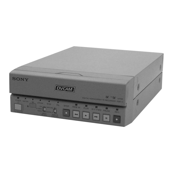
DIGITAL VIDEO CASSETTE RECORDER
DSR-11
RMT-DS11
US Model
Canadian Model
AEP Model
UK Model
Australian Model
New Zealand Model
R MECHANISM
General
Power consumption
15 W (during playback)
Peak inrush current
Hot switching inrush current,
measured in accordance with
European standard EN55103-1:
6 A (230V)
Operating temperature
5 °C to 40 °C (41 °F to 104 °F)
Storage temperature
–20 °C to +60 °C (–4 °F to +140 °F)
– Continued on next page –
Advertisement
Table of Contents

Related Manuals for Sony DVCAM DSR-11


Summary of Contents for Sony DVCAM DSR-11
- Page 1 DSR-11 RMT-DS11 SERVICE MANUAL US Model Canadian Model AEP Model UK Model Ver 1.0 2000. 11 Australian Model New Zealand Model R MECHANISM SPECIFICATIONS Clock System General Quartz locked Recording format DVCAM/DV (SP) format, rotating Power consumption Power back-up Back-up duration: up to one month 15 W (during playback) 2-head helical scan, digital (after a 10-hour charge)
- Page 2 DE FONCTIONNEMENT. NE REMPLACER CES COM- SONY PARTS WHOSE PART NUMBERS APPEAR AS SHOWN IN THIS MANUAL OR IN SUPPLEMENTS PUB- POSANTS QUE PAR DES PIÈCES SONY DONT LES LISHED BY SONY. NUMÉROS SONT DONNÉS DANS CE MANUEL OU DANS LES SUPPLÉMENTS PUBLIÉS PAR SONY.
-
Page 3: Table Of Contents
TABLE OF CONTENTS Section Title Page Section Title Page SERVICE NOTE • JC-20 (DV INTERFACE) Schematic Diagram ..4-33 ............... 5 • JC-20 (MECHANISM CONTROL 1) Schematic Diagram ..........4-35 Note for Repair ............5 • JC-20 (MECHANISM CONTROL 2) Schematic Diagram .......... - Page 4 Section Title Page Section Title Page 3-12. Brake Arm S, Ratchet Brake T, C Page Table ............5-44 Tension Coil Spring (Brake), SBR Slider and FP-248 D Page Table ............5-45 Flexible Board (Condensation Sensor) ....5-14 E Page Table ............5-45 3-13.
-
Page 5: Service Note
SERVICE NOTE When remove a connector, don’t pull at wire of connector. NOTE FOR REPAIR It is possible that a wire is snapped. Make sure that the flat cable and flexible board are not cracked of bent at the terminal. Do not insert the cable insufficiently nor crookedly. -
Page 6: Self-Diagnosis Function
SELF-DIAGNOSIS FUNCTION Self-diagnosis Function Self-diagnosis Display When problems occur while the unit is operating, the time code of When problems occur while the unit is operating, the self-diagno- sis function starts working, and displays on the monitor screen the monitor screen shows a 4-digit display consisting of an alpha- what to do. -
Page 7: Self-Diagnosis Code Table
Self-diagnosis Code Table Self-diagnosis Code Block Detailed Symptom/State Correction Function Code Condensation. Remove the cassette, and insert it again after one hour. Video head is dirty. Clean with the optional cleaning cassette. LOAD direction. Loading does not Load the tape again, and perform operations from the beginning. complete within specified time UNLOAD direction. -
Page 8: General
Digital slow playback Video signals are separated into color difference ..................signals and luminance signals, which are encoded and are trademarks of Sony The unit has a frame memory function that allows compressed to one-fifth size before being recorded to Corporation. - Page 9 CONTROL switch on the front panel to CONTROL S. to zero. Otherwise, you cannot operate the unit with • if you press a counter reset button on a Sony remote 4 PAUSE button CONTROL S-devices. commander while pointing it toward this unit during...
-
Page 10: Notes On Video Cassettes
Location and Function of Parts Chapter 6 REW button Battery installation 7 On/standby switch Push and slide the lid to open. 8 DISPLAY button Playback and Press this button to see indications, such as time code and tape remaining time, on the monitor screen. Recording For details on displayed data, see “Displaying various data”... -
Page 11: Playback
Preparations After checking the tape for slack, hold the cassette so that the tape Notes on Recording/Playback window is facing upward, then insert it into the unit. No compensation for contents of the recording Contents of the recording cannot be compensated for if recording or playback is not successful due to a malfunction of the unit, video tape, etc. - Page 12 VCR. For details on the procedures required when using a computer as a recorder, refer to the instruction manual of your computer If you record on a tape using a Sony digital camcorder (DSR-200/200P, or the user’s manuals of the software installed in it.
- Page 13 For details on the AUDIO SET menu, see “AUDIO SET menu” on page 44 (GB). A chronological list appears on the monitor screen. Note When the command mode of a Sony device / remote commander is set to When selecting INDEX SEARCH VTR 4;...
- Page 14 • Searching may not be done correctly if the signals were not recorded on a want. piece of Sony-brand digital video equipment. About the cassette memory Each time you press the . or > button, the unit searches for the •...
-
Page 15: Recording
Recording Recording Connecting to another VCR This section describes the necessary connections, settings and operations to perform recording on this unit. The same settings and operations apply The video and audio signals are sent from another VCR with virtually no whether you are using the unit for dubbing or as a stand-alone recorder. -
Page 16: Installing The Unit Vertically
Recording Recording Procedure Select an input signal by switching the INPUT SELECT selector on this unit. This section describes the procedures used to record signals sent from DV: to record input signals from the DV IN/OUT connector another VCR to this unit. For details on the procedures required when S VIDEO: to record input signals from the S VIDEO connector on the using a computer as a player, refer to the instruction manual of your INPUT jacks... - Page 17 Operating the Menus Menu Organization Menu Contents The menu of this unit consists of the following menus Initial settings are indicated with rectangles. and submenus. VTR SET menu Submenu Icon/Menu Setting Menu Submenu (page) (page) VTR SET REC MODE (page 43 (GB)) VTR SET REC MODE Switches the recording mode between DVCAM and DV (SP mode only).
- Page 18 Operating the Menus CM SET menu Submenu Icon/Menu Setting (page) CM SET TAPE LABEL 3 Repeat steps 1 and 2. After entering all characters for the tape label, select [SET]. Submenu Icon/Menu Setting (page) Note CM SET CM SEARCH Selects the mode which searches recordings. The unit cannot display the TAPE LABEL screen in the following cases: (page 29 (GB)) ON : Searches recordings using the cassette memory.
-
Page 19: Troubleshooting
(See page 16 (GB)) . You did not set the clock when you turned on the unit. t Set the clock Please check the following before contacting your Sony dealer. CLOCK SET with the menu (See page 49 (GB)) . -
Page 20: Compatibility Of Dvcam And Dv Format
(DF/NDF/including without user bits other than those in the above chart appears, contact user bits) your Sony dealer or local authorized Sony service PAL; EBU time code facility and inform them of the number. (including user bits) 1) There are two modes for audio recording; Lock mode and Unlock mode. In Lock mode, the sampling frequencies of audio and video are synchronized. -
Page 21: Disassembly
DSR-11 SECTION 2 DISASSEMBLY Note: Follow the disassembly procedure in the numerical order given. 2-1. UPPER CASE 2-3. VD-031 BOARD 2 Two screws 7 VD bracket 3 Upper case 3 Two flat cables (CN002, 003) 4 Two screws (PTT2.6 × 5) 1 Three connectors (CN501, 602, 603) 5 VD-031 board... -
Page 22: Board
2-5. HD-024 BOARD 2-7. JC-20 BOARD 4 Four screws 7 Two connectors (T2 × 4.5) (CN300, 501) 9 HD-024 board 5 JC shield case 1 Flat cable (CN5005) 3 Two screws 1 Connector (B2 × 4) (CN100) 6 JC shield case 6 Two flexible boards (CN400, 500 ) 2 Flat cable... -
Page 23: Circuit Boards Location
2-9. CIRCUIT BOARDS LOCATION JC-20 VIDEO A/D CONVERTER, CHROMA MIX, AFC, VIDEO DISP, D/A CONVERTER, SFD, TFD, DV INTERFACE, AUDIO, MECHANISM CONTROL, MODE CONTROL, POWER SUPPLY RP-234 DC-1492 (REC/PB AMP) (DC/DC CONVERTER) VD-031 JD-002 INTERFACE, VIDEO DECODER, DV CONVERTER, VIDEO OUTPUT, AUDIO, CONTROL JACK Y/C SEPARATION JA-006... -
Page 24: Overall Block Diagram 1
DSR-11 SECTION 3 BLOCK DIAGRAMS 3-1. OVERALL BLOCK DIAGRAM 1 VD-031 BOARD JA-006 BOARD (1/2) CN002 (1/2) (SEE PAGE 4-85) IC102 Q117 Y IN FL104 DL101 BUFFER S-Y/Y SWITCH CN101 (SEE PAGE 4-53) (1/2) CN003 (1/2) Y IN J101 (1/2) Q119 CR IN FL103... -
Page 25: Overall Block Diagram 2
DSR-11 3-2. OVERALL BLOCK DIAGRAM 2 JD-002 (1/2) JC-20 BOARD (1/2) JIG PIN BOARD (FOR CHECK) IN/OUT CN4400 CN252 CN253 CN1101 (1/3) IC1108 3 17 Y (8) IC4402 NTPB, CN201 Y IN RP-234 BOARD ı ı TPB, ı CONVERTER NTPA, (SEE PAGE 4-33) (SEE PAGE 4-22) (SEE PAGE 4-88) -
Page 26: Overall Block Diagram 3
DSR-11 3-3. OVERALL BLOCK DIAGRAM 3 M903 CN400 HD-024 BOARD (1/2) JC-20 BOARD CN5005 (1/2) CN001 (1/2) CAP FG CAP FG CAPSTAN FG2, FG1 (2/2) FG AMP CAP FWD, CAP ON CAP FWD, CAP ON DRUM FWD, DRUM ON DRUM FWD, DRUM ON IC400 (SEE PAGE 4-68) DRUM MASTER CLK... -
Page 27: Overall Block Diagram 4
DSR-11 3-4. OVERALL BLOCK DIAGRAM 4 JD-002 BOARD HD-024 BOARD (2/2) FR-175 BOARD (2/2) (SEE PAGE 4-81) (2/2) CN602 CN501 (SEE PAGE4-88) (SEE PAGE 4-61) (2/2) (2/2) S501 CN201 CN705 XEJECT XEJECT LANC VCC LANC VCC IC706 EJECT J201 LANC JK IN LANC LANC DRIVER... -
Page 28: Power Block Diagram 1
DSR-11 3-5. POWER BLOCK DIAGRAM 1 JA-006 BOARD DC-1492 BOARD (SEE PAGE 4-85) L305 Q302 CN102 L401 FB301 L302 Q703 F101 SWITCHING J102 UNREG 12V (1) DC IN SWITCHING L101 F103 L204 UNREG 12V (2) ZD302 HD-024BOARD CN100 L604 F102 UNREG 12V (3) Q301 POWER 2... -
Page 29: Power Block Diagram 2
DSR-11 3-6. POWER BLOCK DIAGRAM 2 HD-024 BOARD IC300 IC400 IC500 IC202 CN500 M901 LOADING CAPSTAN DRUM/C SENSOR VCC REEL FG DRUM MOTOR MOTOR MOTOR MOTOR DRIVE DRIVE DRIVE (SEE PAGE 4-69) (SEE PAGE 4-68) (SEE PAGE 4-68) (SEE PAGE 4-70) CN400 M903 FG VCC... -
Page 30: Power Block Diagram 3
DSR-11 3-7. POWER BLOCK DIAGRAM 3 VD-031 BOARD L001 IC001 +5V REG (SEE PAGE 4-52) L002 CN602 CN603 UNSW 6V UNSW 6V UNSW 6V VIDEO 5V SW 3.1V UNSW 3.1V UNSW 3.1V JC-20 BOARD SW 3.1V SW 3.1V CN1100 DC-1492 BOARD POWER 4 VIDEO –5V VIDEO –5V... -
Page 31: Power Block Diagram 4
DSR-11 3-8. POWER BLOCK DIAGRAM 4 JC-20 BOARD IC1101 IC1103 IC1105 IC1111 IC1108 IC1109 IC1110 IC1107 IC1102 IC1104 IC1106 IC1112 REF. VOLTAGE GEN. REF DC REF DC CONVERTER CONVERTER CONVERTER (SEE PAGE 4-21) BUFFER GEN. GEN. (SEE PAGE 4-22) (SEE PAGE 4-22) (SEE PAGE 4-22) (SEE PAGE 4-20) (SEE PAGE 4-21) -
Page 32: Printed Wiring Boards And Schematic Diagrams
DSR-11 SECTION 4 PRINTED WIRING BOARDS AND SCHEMATIC DIAGRAMS THIS NOTE IS COMMON FOR PRINTED WIRING BOARDS AND SCHEMATIC DIAGRAMS. (In addition to this, the necessary note is printed in each block) For printed wiring boards: Measuring conditions voltege and waveform: •... -
Page 33: Frame Schematic Diagram (1/2)
DSR-11 4-1. FRAME SCHEMATIC DIAGRAM (1/2) FR-175 BOARD (TAPE LED) (CC DOWN) MD-76 BOARD TAPE TOP (C IN) D510 POWER (L/S-CAS) TAPE END D513 S505 S506 S507 S508 S509 S510 S501 CAUTION EJECT S502 D514 ON/STANDBY M904 REEL MOTOR D516 D525 DVCAM M902... -
Page 34: Frame Schematic Diagram (2/2)
DSR-11 FRAME SCHEMATIC DIAGRAM (2/2) CN7001 CN501 A.GND A.GND JA-006 BOARD A.REC_R A.REC_R A.GND A.GND VD-031 JV-062 A.REC_L A.REC_L HARNESS BOARD A.GND CN003 A.GND CN101 A.PB_R A.PB_R N.C. A.GND A.GND AUTOREPEAT AUTOREPEAT A.PB_L A.PB_L NT/XPAL NT/XPAL J101 Y_IN Y_IN CN002 V.GND V.GND CN1101... -
Page 35: Printed Wiring Boards And Schematic Diagrams
DSR-11 4-2. PRINTED WIRING BOARDS AND SCHEMATIC DIAGRAMS RP-234 (REC/PB AMP) PRINTED WIRING BOARD • For Printed Wiring Board. • RP-234 board is six-layer print board. However, the patterns of – Ref. No.: RP-234 board; 30,000 series – layers 2 to 5 have not been included in the diagram. •... - Page 36 DSR-11 REC/PB AMP 4-10 RP-234...
- Page 37 DSR-11 RP-234 (REC/PB AMP 1) SCHEMATIC DIAGRAM • See page 4-7 for RP-234 printed wiring board. • See page 4-95 for waveforms. RP-234 BOARD (1/2) REC/PB AMP 1 -REF.NO.:30,000 SERIES- RF6V XX MARK:NO MOUNT NO MARK:REC/PB MODE R:REC MODE P:PB MODE RP-234 BOARD (2/2) CN203 CL205...
- Page 38 DSR-11 RP-234 (REC/PB AMP 2) SCHEMATIC DIAGRAM • See page 4-7 for RP-234 printed wiring board. • See page 4-95 for waveforms. RP-234 BOARD (2/2) REC/PB AMP 2 -REF.NO.:30,000 SERIES- XX MARK:NO MOUNT NO MARK:REC/PB MODE R:REC MODE P:PB MODE RF6V RP-234 BOARD (1/2) L202...
- Page 39 DSR-11 JC-20 (VIDEO PB AMP, VIDEO A/D CONVERTER, CHROMA MIX, AFC, VFD, SFD, TFD, DV INTERFACE, MECHANISM CONTROL, AUDIO, POWER SUPPLY) PRINTED WIRING BOARD – Ref. No.: JC-20 board; 20,000 series – • For Printed Wiring Board. • JC-20 board is six-layer print board. However, the patterns of layers 2 to 5 have not been included in the diagram.
- Page 40 DSR-11 14 15 4-17 4-18 VIDEO PB AMP, VIDEO A/D CONVERTER, CHROMA MIX, AFC, VFD, SFD, TFD, DV INTERFACE, MECHANISM CONTROL, AUDIO, POWER SUPPLY JC-20...
- Page 41 DSR-11 JC-20 (VIDEO PB AMP) SCHEMATIC DIAGRAM • See page 4-15 for JC-20 printed wiring board. • See page 4-95 for waveforms. JC-20 BOARD (1/14) VIDEO PB AMP -REF.NO.:20,000 SERIES- XX MARK:NO MOUNT NO MARK:REC/PB MODE AFC_Y JC-20 BOARD (4/14) Y_IN JC-20 BOARD (14/14) CR_IN...
-
Page 42: Video A/D Converter) Schematic Diagram
DSR-11 JC-20 (VIDEO A/D CONVERTER) SCHEMATIC DIAGRAM • See page 4-15 for JC-20 printed wiring board. • See page 4-95 for waveforms. JC-20 BOARD (2/14) VIDEO A/D CONVERTER SPCK1 JC-20 BOARD (4/14) JC-20 BOARD (14/14) VIDEO_-5V C1180 R1211 L1114 -REF.NO.:20,000 SERIES- 10uH XX MARK:NO MOUNT C1159... - Page 43 DSR-11 JC-20 (CHROMA MIX) SCHEMATIC DIAGRAM • See page 4-15 for JC-20 printed wiring board. JC-20 BOARD (3/14) CHROMA MIX -REF.NO.:20,000 SERIES- XX MARK:NO MOUNT NO MARK:REC/PB MODE R:REC MODE P:PB MODE IC2214 IC2214 IC2215 IC2209 TC74VHC374FT(EL) TC74VHC244FT(EL) R2250 IC2215 TC74VHC541FT(EL) R1.4/P3.2 IC2212...
-
Page 44: Afc) Schematic Diagram
DSR-11 JC-20 (AFC) SCHEMATIC DIAGRAM • See page 4-15 for JC-20 printed wiring board. • See page 4-95, 96 for waveforms. JC-20 BOARD (4/14) -REF.NO.:20,000 SERIES- NO MARK:REC/PB MODE R:REC MODE XX MARK:NO MOUNT P:PB MODE 17-2 R2253 17-1 R2256 CL2236 JC-20 BOARD (3/14) 17-3... -
Page 45: Vfd (Video Dsp, D/A Converter)) Schematic Diagram
DSR-11 JC-20 (VFD (VIDEO DSP, D/A CONVERTER)) SCHEMATIC DIAGRAM • See page 4-15 for JC-20 printed wiring board. • See page 4-96 for waveforms. JC-20 BOARD (5/14) VFD(VIDEO DSP,D/A CONVERTER) -REF.NO.:20,000 SERIES- XX MARK:NO MOUNT NO MARK:REC/PB MODE R:REC MODE P:PB MODE L3302 R3310... -
Page 46: Sfd) Schematic Diagram
DSR-11 JC-20 (SFD) SCHEMATIC DIAGRAM • See page 4-15 for JC-20 printed wiring board. • See page 4-96 for waveforms. JC-20 BOARD (6/14) -REF.NO.:20,000 SERIES- XX MARK:NO MOUNT NO MARK:REC/PB MODE R:REC MODE P:PB MODE 39-1 C4410 C4411 39-2 R4409 X4400 24.576MHz TDO3... -
Page 47: Tfd) Schematic Diagram
DSR-11 JC-20 (TFD) SCHEMATIC DIAGRAM • See page 4-15 for JC-20 printed wiring board. JC-20 BOARD (7/14) NO MARK:REC/PB MODE -REF.NO.:20,000 SERIES- R:REC MODE P:PB MODE XX MARK:NO MOUNT RF_6V JC-20 BOARD (9/14) JC-20 BOARD (8/14) 41-1 CN4401 RF 6V RF 6V C1ERRP C4420... -
Page 48: Dv Interface) Schematic Diagram
DSR-11 JC-20 (DV INTERFACE) SCHEMATIC DIAGRAM • See page 4-15 for JC-20 printed wiring board. JC-20 BOARD (8/14) DV INTERFACE -REF.NO.:20,000 SERIES- R4430 R4425 XX MARK:NO MOUNT NO MARK:REC/PB MODE R:REC MODE P:PB MODE 39-1 39-2 LBUS3 XDVCN LBUS2 XRST_PHY LBUS1 R3.1/P2.1 LIP_SLEEP... -
Page 49: Mechanism Control 1) Schematic Diagram
DSR-11 JC-20 (MECHANISM CONTROL 1) SCHEMATIC DIAGRAM • See page 4-15 for JC-20 printed wiring board. JC-20 BOARD (9/14) MECHANISM CONTROL 1 NO MARK:REC/PB MODE -REF.NO.:20,000 SERIES- R:REC MODE P:PB MODE XX MARK:NO MOUNT RF_6V L5001 JC-20 BOARD (7/14) 10uH J_3V J_3V JC-20 BOARD (10/14) -
Page 50: Mechanism Control 2) Schematic Diagram
DSR-11 JC-20 (MECHANISM CONTROL 2) SCHEMATIC DIAGRAM • See page 4-15 for JC-20 printed wiring board. • See page 4-96 for waveforms. JC-20 BOARD (10/14) MECHANISM CONTROL 2 -REF.NO.:20,000 SERIES- XX MARK:NO MOUNT NO MARK:REC/PB MODE R:REC MODE P:PB MODE J_3V IC5008 *:IMPOSSIBLE TO MEASURE THE... -
Page 51: Mode Control) Schematic Diagram
DSR-11 JC-20 (MODE CONTROL) SCHEMATIC DIAGRAM • See page 4-15 for JC-20 printed wiring board. • See page 4-96 for waveforms. JC-20 BOARD (11/14) MODE CONTROL -REF.NO.:20,000 SERIES- XX MARK:NO MOUNT Q6003 NO MARK:REC/PB MODE UN9113J-(K8).SO R:REC MODE P:PB MODE R6057 R6059 MO73... -
Page 52: Audio 1) Schematic Diagram
DSR-11 JC-20 (AUDIO 1) SCHEMATIC DIAGRAM • See page 4-15 for JC-20 printed wiring board. JC-20 BOARD (12/14) AUDIO 1 -REF.NO.:20,000 SERIES- XX MARK:NO MOUNT Note:Ferrite beads are mounted to the IC7005 location where R7009,R7010,R7013 and R7015 are printed. NO MARK:REC/PB MODE J_3V R7009 JC-20 BOARD (14/14) - Page 53 DSR-11 JC-20 (AUDIO 2) SCHEMATIC DIAGRAM • See page 4-15 for JC-20 printed wiring board. • See page 4-96 for waveforms. JC-20 BOARD (13/14) AUDIO 2 -REF.NO.:20,000 SERIES- XX MARK:NO MOUNT NO MARK:REC/PB MODE CN7002 CL7004 AU X1 IN AU_X1_IN CL7005 AU_Y1_IN AU Y1 IN...
-
Page 54: Power Supply) Schematic Diagram
DSR-11 JC-20 (POWER SUPPLY) SCHEMATIC DIAGRAM • See page 4-15 for JC-20 printed wiring board. JC-20 BOARD (14/14) POWER SUPPLY -REF.NO.:20,000 SERIES- XX MARK:NO MOUNT NO MARK:REC/PB MODE J_3V JC-20 BOARD (11/14) J_3V JC-20 BOARD (12/14) CN1100 CL1100 CL1182 UNSW 6V J_1.9V CL1101 UNSW 3.1V... -
Page 55: Printed Wiring Board
DSR-11 VD-031 (INTERFACE, VIDEO DECODER, VIDEO OUTPUT, AUDIO, Y/C SEPARATION) PRINTED WIRING BOARD – Ref. No.: VD-031 board; 50,000 series – • For Printed Wiring Board. • There are a few cases that the part isn't mounted in this model is printed on this diagram. - Page 56 DSR-11 CL126 CL103 CL039 CL040 CL108 CL114 CL113 CL124 CL125 CL111 4-50 INTERFACE, VIDEO DECODER, VIDEO OUTPUT, AUDIO, Y/C SEPARATION 4-49 VD-031...
-
Page 57: Interface) Schematic Diagram
DSR-11 VD-031 (INTERFACE) SCHEMATIC DIAGRAM • See page 4-47 for VD-031 printed wiring board. VD-031 BOARD (1/5) INTERFACE -REF.NO.:50,000 SERIES- XX MARK:NO MOUNT VD-031 BOARD (4/5) UNSW_6V NO MARK:REC/PB MODE SW_3.1V JC-20 BOARD (1/14) VD-031 BOARD (2/5) CN1101 CN602 CL631 VIDEO_5V (THROUGH THE FJV-001 FLAT CABLE) UNSW_6V... -
Page 58: Video Decoder) Schematic Diagram
DSR-11 VD-031 (VIDEO DECODER) SCHEMATIC DIAGRAM • See page 4-47 for VD-031 printed wiring board. • See page 4-97 for waveforms. VD-031 BOARD (2/5) VIDEO DECODER -REF.NO.:50,000 SERIES- Q126 Q124 L109 2SC4081T106R 10uH 2SC4081T106R XX MARK:NO MOUNT NO MARK:REC/PB MODE Q117 Q121 R204... -
Page 59: Video Output) Schematic Diagram
DSR-11 VD-031 (VIDEO OUTPUT) SCHEMATIC DIAGRAM • See page 4-47 for VD-031 printed wiring board. • See page 4-97 for waveforms. SIGNAL PATH VD-031 BOARD (3/5) VIDEO SIGNAL FB300 C OUT CHROMA Y/CHROMA VIDEO OUTPUT IC301 -REF.NO.:50,000 SERIES- C306 C311 4.7u 0.1u XX MARK:NO MOUNT... -
Page 60: Audio) Schematic Diagram
DSR-11 VD-031 (AUDIO) SCHEMATIC DIAGRAM • See page 4-47 for VD-031 printed wiring board. SIGNAL PATH VD-031 BOARD (4/5) AUDIO SIGNAL AUDIO -REF.NO.:50,000 SERIES- XX MARK:NO MOUNT NO MARK:REC/PB MODE AUDIO_5V C531 C511 100u R512 6.3V 6.3V 1500 AUDIO_GND VD-031 BOARD (1/5) C532 100u IC502... -
Page 61: Y/C Separation) Schematic Diagram
DSR-11 VD-031 (Y/C SEPARATION) SCHEMATIC DIAGRAM • See page 4-47 for VD-031 printed wiring board. • See page 4-97 for waveforms. VD-031 BOARD (5/5) L701 Y/C SEPARATION 10uH L707 -REF.NO.:50,000 SERIES- 10uH XX MARK:NO MOUNT RV702 C711 R719 C702 C719 RV702 0.1u 3900... -
Page 62: Hi Control) Schematic Diagram
DSR-11 HD-024 (HI CONTROL) SCHEMATIC DIAGRAM • See page 4-71 for HD-024 printed wiring board. • See page 4-98 for waveforms. HD-024 BOARD (1/5) IC706 HI CONTROL C709 0.1u -REF.NO.:40,000 SERIES- Q701 R715 XX MARK:NO MOUNT UN5111-TX CL724 C711 2700 0.1u NO MARK:REC/PB MODE C715... -
Page 63: Matrix Key Control, Led Drive) Schematic Diagram
DSR-11 HD-024 (MATRIX KEY CONTROL, LED DRIVE) SCHEMATIC DIAGRAM • See page 4-71 for HD-024 printed wiring board. HD-024 BOARD (2/5) MATRIX KEY CONTROL,LED DRIVE NO MARK:REC/PB MODE R:REC MODE -REF.NO.:40,000 SERIES- P:PB MODE XX MARK:NO MOUNT *:IMPOSSIBLE TO MEASURE THE VOLTAGE AT THE MARKED POINTS. -
Page 64: Uvic) Schematic Diagram
DSR-11 HD-024 (UVIC) SCHEMATIC DIAGRAM • See page 4-71 for HD-024 printed wiring board. • See page 4-98 for waveforms. HD-024 BOARD (3/5) UVIC -REF.NO.:40,000 SERIES- XX MARK:NO MOUNT NO MARK:REC/PB MODE R:REC MODE R562 P:PB MODE R553 R557 Q551 Q552 Q555 2SC2712Y-... -
Page 65: Dc/Dc Converter, Capstan Motor Drive, Cam Motor Drive) Schematic Diagram
DSR-11 HD-024 (DC/DC CONVERTER, CAPSTAN MOTOR DRIVE, CAM MOTOR DRIVE) SCHEMATIC DIAGRAM • See page 4-71 for HD-024 printed wiring board. • See page 4-98 for waveforms. IC400 HD-024 BOARD (4/5) DC/DC CONVERTER,CAPSTAN MOTOR DRIVE,CAM MOTOR DRIVE CN400 CL404 FG VCC -REF.NO.:40,000 SERIES- XX MARK:NO MOUNT IC400... -
Page 66: Drum Motor Drive, Fl Motor Drive, Reel Motor Drive) Schematic Diagram
DSR-11 HD-024 (DRUM MOTOR DRIVE, FL MOTOR DRIVE, REEL MOTOR DRIVE) SCHEMATIC DIAGRAM • See page 4-71 for HD-024 printed wiring board. • See page 4-98 for waveforms. SIGNAL PATH HD-024 BOARD (5/5) REC/PB DRUM MOTOR DRIVE,FL MOTOR DRIVE,REEL MOTOR DRIVE Drum speed servo -REF.NO.:40,000 SERIES- XX MARK:NO MOUNT... -
Page 67: Printed Wiring Board
DSR-11 HD-024 (HI CONTROL, MATRIX KEY CONTROL, LED DRIVE, DC/DC CONVERTER, MOTOR DRIVE) PRINTED WIRING BOARD – Ref. No.: HD-024 board; 40,000 series – • For Printed Wiring Board. • There are a few cases that the part isn't mounted in this model is printed on this diagram. - Page 68 DSR-11 4-74 HI CONTROL, MATRIX KEY CONTROL, LED DRIVE, DC/DC CONVERTER, MOTOR DRIVE 4-73 HD-024...
-
Page 69: Printed Wiring Board
DSR-11 MD-76 (TAPE SENSOR) PRINTED WIRING BOARD • For Printed Wiring Board. • MD-76 board is four-layer print board. However, the patterns of – Ref. No.: MD-76 board; 30,000 series – layers 2 to 3 have not been included in the diagram. •... -
Page 70: Schematic Diagram
VOLTAGE AT THE MARKED POINTS. HD-024 BOARD(5/5) CN200 THROUGH THE FMD-14 FLAT CABLE (SEE PAGE 4-69) M904 REEL MOTOR GAIN GAIN OFFSET OFFSET HD-024 BOARD(5/5) CN201 THROUGH THE FMD-14 FLAT CABLE (SEE PAGE 4-69) TLP907 (LB, SONY) TLP907(LB, SONY) TAPE SENSOR 4-77 4-78 MD-76... -
Page 71: Printed Wiring Board
DSR-11 FR-175 (USER CONTROL) PRINTED WIRING BOARD • For Printed Wiring Board. • There are a few cases that the part isn't mounted in this model – Ref. No.: FR-157 board; 30,000 series – is printed on this diagram. • See page 4-100 for printed parts location. •... - Page 72 DSR-11 FR-175 (USER CONTROL) SCHEMATIC DIAGRAM FR-175 BOARD USER CONTROL -REF.NO.:30,000 SERIES- XX MARK:NO MOUNT NO MARK:REC/PB MODE CN501 CL534 D526 D518 D522 D531 D536 D537 1SS367-T3SONY 1SS367-T3SONY 1SS367-T3SONY 1SS367-T3SONY 1SS367-T3SONY 1SS367-T3SONY CL533 KEY1 KEY1 CL532 KEY2 KEY2 S505 S506 S507 S508 S509...
-
Page 73: Printed Wiring Board
DSR-11 JA-006 (AV IN/OUT, DC IN) PRINTED WIRING BOARD – Ref. No.: JA-006 board; 10,000 series – • For Printed Wiring Board. • There are a few cases that the part isn't mounted in this model is printed on this diagram. •... -
Page 74: Schematic Diagram
DSR-11 JA-006 (AV IN/OUT, DC IN) SCHEMATIC DIAGRAM JA-006 BOARD AV IN/OUT,DC IN -REF.NO.:10,000 SERIES- XX MARK:NO MOUNT S102 AUTO_REPEAT D113 1 MK 01ZA8.2(TPL3) 2 COM 3 BR S101 1 MK NTSC/PAL 2 COM C101 NTSC 0.1u 3 BR D101 01ZA8.2(TPL3) C102 0.1u... - Page 75 DSR-11 JD-002 (DV CONNECTOR, CONTROL JACK) PRINTED WIRING BOARD AND SCHEMATIC DIAGRAM – Ref. No.: JD-002 board; 10,000 series – • For Printed Wiring Board. • There are a few cases that the part isn't mounted in this model is printed on this diagram. SIGNAL PATH JD-002 BOARD VIDEO SIGNAL...
- Page 76 DSR-11 DC-1492 (DC/DC CONVERTER) SCHEMATIC DIAGRAM • See page 4-91 for DC-1492 printed wiring board. DC-1492 BOARD L604 R701 DC/DC CONVERTER 4.7uH R704 R707 R724 -REF.NO.:60,000 SERIES- C701 2.2k 2.2k ZD701 0.1u UDZ-TE-17-10B Note:Resistor is mounted to the XX MARK:NO MOUNT location where JC701 is printed.
-
Page 77: Dc-1492 Printed Wiring Board
DSR-11 DC-1492 (DC/DC CONVERTER) PRINTED WIRING BOARD – Ref. No.: DC-1492 board; 60,000 series – • For Printed Wiring Board. • There are a few cases that the part isn't mounted in this model is printed on this diagram. • See page 4-101 for printed parts location. •... - Page 78 DSR-11 DC/DC CONVERTER 4-93 4-94 DC-1492...
-
Page 79: Waveforms
4-3. WAVEFORMS RP-234 BOARD JC-20 BOARD 780 mVp-p 3.1 Vp-p 2.8 Vp-p 3.0 Vp-p 3.2 Vp-p 150 Hz 13.5 MHz 0.15 µsec IC301 ra REC/PB IC1112 1 REC/PB IC1109 1 – 8 REC IC2204 qk, w; REC/PB IC5003 <zzm> REC/PB 2.8 Vp-p 560 mVp-p 950 mVp-p... - Page 80 VD-031 BOARD HD-024 BOARD 1.5 Vp-p 1.4 Vp-p 3.2 Vp-p 230 mVp-p 1.1 Vp-p 20 MHz 150 Hz Q110 E REC IC106 5 REC IC701 wg REC IC707 ra REC/PB IC500 4 REC/PB 760 mVp-p 2.1 Vp-p 2.1 Vp-p 850 mVp-p (NTSC) 14.318 MHz (NTSC) 900 mVp-p...
-
Page 81: Parts Location
4-4. PARTS LOCATION RP-234 BOARD RP-234 BOARD JC-20 BOARD JC-20 BOARD VD-031 BOARD HD-024 BOARD HD-024 BOARD MD-76 BOARD MD-76 BOARD FR-175 BOARD FR-175 BOARD JA-006 BOARD JA-006 BOARD (SIDE A) (SIDE B) (SIDE A) (SIDE B) (SIDE A) (SIDE A) (SIDE B) (SIDE A) (SIDE B) - Page 82 DC-1492 BOARD DC-1492 BOARD (SIDE A) (SIDE B) D101 A-10 D102 B-10 D401 D402 IC101 C-10 IC401 D201 Q101 D202 B-10 Q401 D301 Q701 D302 Q706 Q707 IC201 C-10 Q709 IC301 IC801 ZD101 ZD102 B-10 Q102 ZD401 Q201 ZD402 Q202 ZD703 Q301 Q302...
-
Page 83: Adjustments
DSR-11 SECTION 5 ADJUSTMENTS Before starting adjustment EVR Data Re-writing Procedure When Replacing Board The data that is stored in the repair board, is not necessarily correct. Perform either procedure 1 or procedure 2 or procedure 3 when replacing board. Procedure 1 Save the EVR data of the machine in which a board is going to be replaced. -
Page 84: Adjusting Items When Replacing Main Parts And Boards
1-1. Adjusting items when replacing main parts and boards • Adjusting items when replacing main parts When replacing main parts, adjust the items indicated by z in the following table. Replaced part Block Mounted part replacement replacement Adjustment Section Adjustment System control Initialization of C, D, E page data Node unique ID No. - Page 85 • Adjusting items when replacing a board or EEPROM When replacing a board or EEPROM, adjust the items indicated by z in the following table. Replaced part Board replcement Adjustment Section Adjustment System control Initialization of C, D, E page data Node unique ID No.
-
Page 86: Information (Mechanical Section)
1-2. Information (Mechanical Section) -
Page 87: Mechanical Section Adjustments
5-1. MECHANICAL SECTION ADJUSTMENTS 5-1-1. PARTS REPLACEMENT AND PREPARATION FOR ADJUSTMENT 1-1. ASSEMBLY/DISASSEMBLY OF CASSETTE COMPARTMENT For details on disassembling the mechanism deck (R mechanism), refer to the Service Manual of the main unit in which the R mechanism is mounted. Before attaching or removing the cassette compartment, check the position of “L cassette”. -
Page 88: List Of Service Tools
1-3. LIST OF SERVICE TOOLS J-1. Cleaning fluid J-2. Wiping cloth J-3. Super fine applicator J-4. Mirror (Small oval type) (9-919-573-01) (7-741-900-53) (Made by NIPPON (J-6080-840-A) APPLICATOR (P752D)) (J-2501-023-A) J-5. Screwdriver for tape path J-6. Tracking tape (XH2-1A1) J-7. Mini DV torque cassette J-8. -
Page 89: About Mode Selector Ii
1-4. About Mode Selector II • About Mode Selector II 4-1. OUTLINE 4-2. MECHANISM CONDITION (POSITION) This unit is a mechanism drive tool which supplements the main- SHIFTING ORDER LIST tenance of each mechanism deck. Its functions are described below. After selecting the mechanism deck, select one of the two test modes other than the auto test, and press the RVS or FF button to 1. -
Page 90: Periodic Check
5-1-2. PERIODIC CHECK • Carry out the following maintenance and periodic checks not only to fully display the functions and performance of the set, but also for the equipment and tape. After replacing, service the set as follows, regardless of the length of use. 2-1. -
Page 91: Parts Replacement
5-1-3. PARTS REPLACEMENT • Precaution For details on disassembling the cabinets, boards and other parts, refer to “Section 2, Disassembly”. For details on replacing parts (disassembly, assembly) of the mechanism deck, refer to “Information” on page 5-4. 3-1. TAPE GUIDE 1/8 AND GUIDE GUARD Disassembly/Assembly When the tape guide 1/8 is replaced or attached, perform each adjustment from Adjustment Start -2 of the flowchart on page 5-... -
Page 92: Capstan Cover
3-3. CAPSTAN COVER 3-4. REEL MOTOR Disassembly/Assembly Disassembly/Assembly Screw Tightening torque of capstan cover Tightening torque of reel motor 0.3432 ± 0.0196 N • m (3.5 ± 0.2 kg • cm) 0.0686 ± 0.0098 N • m (0.7 ± 0.1 kg • cm) Claw Fasten the screws Screw... -
Page 93: Gl Arm S Assembly, Gl Arm T Assembly, Coaster S Assembly And Coaster T Assembly
3-6. GL ARM S ASSEMBLY, GL ARM T ASSEMBLY, COASTER S ASSEMBLY AND COASTER T ASSEMBLY Disassembly: Remove the parts in order of 1,2,3,4,5,6,7,8,9,0 For the disassembling and assembling procedures of the GL gear, GL helical torsion spring, etc., refer to page 5-21. Move the TG2/7 arms to the loading position with the regulated power supply or by hand while referring to page 5-5. -
Page 94: Mic Base Guide, Mic Base Assembly And Mic Base Spring
3-7. MIC BASE GUIDE, MIC BASE ASSEMBLY AND MIC BASE SPRING Disassembly/Assembly Remove the six solders on the FP-104 flexible board from the rear of the chassis. Pass the flexible board through For the disassembling and assembling procedures of the compo- hole A and pull it out of the front side of the chassis while nents of the MIC base assembly, refer to page 5-21. -
Page 95: Pinch Arm Assembly
3-9. PINCH ARM ASSEMBLY 3-10. CAPSTAN MOTOR Disassembly/Assembly Disassembly/Assembly For the disassembling and assembling procedures of the tape re- (After assembling, adjust the tape path from page 5-23.) tainer and compression coil spring (tape retainer), refer to page 5- Roller Capstan motor Roller Pinch arm assembly... -
Page 96: Brake Arm S, Ratchet Brake T
3-12. BRAKE ARM S, RATCHET BRAKE T, TENSION COIL SPRING (BRAKE), SBR SLIDER AND FP-248 FLEXIBLE BOARD (CONDENSATION SENSOR) Disassembly: Remove them in order of 1,2,3,4 Remove the SBR slider while being careful not Portion of the SBR slider (To attach them, perform the disassembly steps in reverse order.) to touch the adjuster. -
Page 97: Reel Base Retainer, Reel Base T Assembly And Reel Base S Assembly (Reel Lock Release Block And Reel Lock Release Spring)
3-14. REEL BASE RETAINER, REEL BASE T ASSEMBLY AND REEL BASE S ASSEMBLY (REEL LOCK RELEASE BLOCK AND REEL LOCK RELEASE SPRING) Disassembly: Remove them in order of 1,2,3 Assembly: Attach them in order of 1,2,3 1 Move the reel selector slider in the direction of arrow A to (Refer to Assembly, too.) check that the reel selector lever is “L cassette”. -
Page 98: Tg2/7 Arm Block, Tg2/7 Band Block And Tension Coil Spring (Tg2)/(Tg7)
3-16. TG2/7 ARM BLOCK, TG2/7 BAND BLOCK AND TENSION COIL SPRING (TG2)/(TG7) Disassembly: Remove them in order of 1,2,3,4 For the disassembling and assembling procedures of the assembly Notes during work components of the TG2/TG7 arm, refer to page 5-22. Be careful when handling the TG arm and the peripheral parts. -
Page 99: Sub-Slider Arm, Sub-Slider, Encoder Gear, Main Cam Gear, Coupling Gear, Sub-Cam Gear, Pinch Slider And Loading Arm Assembly
3-17. SUB-SLIDER ARM, SUB-SLIDER, ENCODER GEAR, MAIN CAM GEAR, COUPLING GEAR, SUB-CAM GEAR, PINCH SLIDER AND LOADING ARM ASSEMBLY Disassembly: Remove them in order of 1,2,3,4,5,6,7,8 Disassembly of the pinch slider Move the pinch slider to the leftmost end, and Pinch slider slide it upward and remove it when two shafts A are superimposed on the holes of the pinch... - Page 100 4 Apply grease to the fixing block (shaft J and U-shaped groove [Front side of chassis] K) of the coupling gear and portion L of the sub-cam gear (half size of one grain of rice for each part). (Fig. 8) 5 Attach the coupling gear.
-
Page 101: Main Slider, Main Slider Arm And Pendulum Stopper Assembly
3-18. MAIN SLIDER, MAIN SLIDER ARM AND PENDULUM STOPPER ASSEMBLY Disassembly: Remove them in order of 1,2,3 Disassembly of each part The main slider controls several parts. Before removing the main slider, remove “Brake arm S” at the front of the chassis while re- Main slider ferring to “Information”... -
Page 102: Board And Encoder Retainer
3-19. MD-76 BOARD AND ENCODER RETAINER Disassembly: Remove them in order of 1,2,3,4,5,6,7,8,9 Disassembly of MD-76 board Screw Peel off the FP-248 flexible board at the front of the chas- MD-76 board sis (refer to page 5-14). Remove the six solders on the FP-104 flexible board from the rear of the chassis. -
Page 103: Components Of Gl Arm S/T Assembly (Gl Arm Assembly, Gl Helical Torsion Spring, Gl Gear)
3-20. COMPONENTS OF GL ARM S/T ASSEMBLY (GL ARM ASSEMBLY, GL HELICAL TORSION SPRING, GL GEAR) Disassembly and distinguishing the S side from the T side Assembly 1 Attach each GL helical torsion spring to the GL gear. To distinguish the S side from the T side when the opening of the One phase adjustment hole spring tip is facing toward the front, note that the coil tip of the S side is located on the left and that of the T side is located on... -
Page 104: Components Of Drum Assembly (Motor Fpc Assembly, Elastic Connector)
3-22. COMPONENTS OF DRUM ASSEMBLY (MOTOR FPC ASSEMBLY, ELASTIC CONNECTOR) Disassembly/Assembly Connect the elastic connector to the drum assembly and attach the motor FPC assembly while aligning pin B with hole C of the drum assembly. Fix the supporter plate with the screws while being careful of pin A of the motor FPC assembly. -
Page 105: Check And Adjustment
5-1-4. CHECK AND ADJUSTMENT • When the parts of the tape path (tape guide, reel table, etc.) have been removed or parts have been replaced, adjust the following parts according to the flowchart below. • ADJUSTMENT POSITION (Tracking entrance, curl) (Tracking exit, curl) (TG2 height/FWD height, curl) (TG7 height/RVS position, curl) -
Page 106: Reel Table Height Check And Adjustment
4-1. REEL TABLE HEIGHT CHECK AND ADJUSTMENT 1. Preparation before check 2. Check and adjustment Check that the cassette compartment has already been removed. Put the reel reference plate (J-12) on each reel table. Rotate the (Refer to page 5-5.) screw block of the reel table so that the height of the cassette ref- Fit the cassette reference plate (J-11) in the cassette positioning erence plate is the same as that of the reel reference plate. -
Page 107: Tg2/7 Height Check And Adjustment
4-3. TG2/7 HEIGHT CHECK AND ADJUSTMENT 1. Preparation before check 2. Check and adjustment Check that the cassette compartment block has already been Rotate the TG upper flange until the height of the TG2/7 preset removed. (Refer to page 5-5.) plate (J-13) and TG2 or TG7 roller block is the same. -
Page 108: Electric Tension Regulator Check And Adjustment Of Tg2/7 Arm
4-5. ELECTRIC TENSION REGULATOR CHECK AND ADJUSTMENT OF TG2/7 ARM 1. Preparation before check 1) Check that the cassette compartment block has already been Attach the cassette reference plate (J-11) and TG2/7 preset plate removed. (Refer to page 5-5.) (J-13). (Refer to page 5-25.) 2) Set the mechanism deck to the loading end position (TG2 to 7 Connect the relay board for tension regulator adjustment (J- already moved to the loading end position and the pinch roller... -
Page 109: Fwd/Rvs Back Tension Check And Adjustment
4-6. FWD/RVS BACK TENSION CHECK AND ADJUSTMENT 1. Preparation before check 2. Check and adjustment Mount the mechanism deck in the main unit, connect all the con- • FWD (TG2) side The torque value should satisfy 9.5 ± 1.5 × 10 nectors, then insert the mini DV torque cassette (J-7) into the mN •... -
Page 110: Preparation For Adjustment And Tape Path Check
4-7. PREPARATION FOR ADJUSTMENT AND TAPE PATH CHECK Preparation before adjustment (connection and setting) Tape path check (checking the RF waveform) Mount the mechanism deck in the main unit. Play back the tracking tape (J-6) and check the states at the en- (Connect all the connectors.) trance and exit of the RF waveform. -
Page 111: Track Adjustment And Check (Checking The Rf Waveform)
4-8. TRACK ADJUSTMENT AND CHECK (Checking the RF Waveform) • Checking the RF waveform • If not flat Check that the RF waveforms at both the entrance and exit are flat If the waveform at the entrance is bad, rotate TG3. If the wave- while the tracking tape (J-6) runs in the PLAY mode. -
Page 112: Cue/Rev Check
4-10. CUE/REV CHECK • Check Check that the intervals of the waveform peaks are consistent while the tracking tape (J-6) runs in the CUE mode or REV mode. [Waveform in CUE or REV mode] The intervals of the waveform peaks must be consistent. -
Page 113: Rising Check
4-12. RISING CHECK • Check • Check that the tape loads and unloads smoothly. Check that when the tracking tape (J-6) is switched from the STOP, • Play a self-recorded or already recorded tape, and check that CUE, REV, FF, REW modes to the PLAYBACK mode, the wave- the sound and images are normal. -
Page 114: Service Mode
5-2. SERVICE MODE • Changing the address The address increases when the FF (M) button is pressed, 5-2-1. ADJUSTING REMOTE COMMANDER and decreases when the REW (m) button is pressed. There are altogether 256 addresses, from 00 to FF. The adjusting remote commander is used for changing the calcu- •... -
Page 115: Data Processing
5-2-2. DATA PROCESSING The calculation of the adjusting remote commander display data (hexadecimal notation) are required for obtaining the adjustment data of some adjustment items. In this case, after converting the hexadecimal notation to decimal notation, calculate and convert the result to hexadecimal notation, and use it as the adjustment data. -
Page 116: Service Mode
5-2-3. SERVICE MODE 2. Emergence Memory Address 1. Setting the Test Mode Page C Address 38 to 43 Page E Address 10 Address Contents EMG code when first error occurs Data Function Upper: MSW code when shift starts when first error Normal occurs Lower: MSW code when first error occurs... -
Page 117: Emg Code (Emergency Code)
3. EMG Code (Emergency Code) Codes corresponding to the errors which occur are written in ad- dresses 38, 3C, 3E. The type of error indicated by the code are shown in the following table. Code Error Type No error (Initial state) Loading motor time-out during LOAD Loading motor time-out during UNLOAD Error during tape take up... - Page 118 5. Bit Value Discrimination Display on the Bit values Bit values must be discriminated using the display data of the ad- adjustment bit3 bit2 bit1 bit0 justment remote commander for the following items. Us the table remote below to discriminate if the bit value is “1” or “0”. commander bit7 bit6...
-
Page 119: Record Of Use Check
6. Record of Use Check Page E Address D0 to E3 Address Function Remark OPRATION 1 Lower two digits The cumulative total hours of operating time is displayed. Higher two digits DRUM RUN 1 Lower two digits The cumulative total hours of drum rotation with tape threaded is displayed. Higher two digits TAPE RUN 1 Lower two digits... -
Page 120: Video Section Adjustments
5-3. VIDEO SECTION ADJUSTMENTS When performing adjustments, refer to the layout diagrams for adjustment related parts on page 5-60, 61. 3-1. PREPARATIONS BEFORE ADJUSTMENT 3-1-1. Equipment Used 1) TV monitor 2) Oscilloscope with 2-phenomenon, 30 MHz band, and delay mode (Unless specified otherwise, use a 10 : 1 probe) 3) Frequency counter 4) Digital voltmeter 5) Audio generator... -
Page 121: Connection Of Equipment
3-1-2. Connection of Equipment Note 1: In adjustments specifying for the S VIDEO input to be According to the specification for the input terminal (S VIDEO used, using the VIDEO input would disable the product input or VIDEO input), connect measuring equipment as shown in specifications of this unit from being satisfied. -
Page 122: Checking The Input Signals
3-1-3. Checking the Input Signals 2. VIDEO Input Because the video signal obtained from the pattern generator is Connect the oscilloscope to the VIDEO input terminal, and check used as the adjustment signal for adjustments, the video output that the sync signal amplitude of the video signal is approximately signal must satisfy the given specifications. -
Page 123: Adjustment Tapes
3-1-4. Adjustment Tapes Use the alignment tapes shown in the following table. Use tapes specified in the signal column of each adjustment. Name Switching position SW/OL standard (XH2-3) adjustment Audio operation check Audio system adjustment (XH5-3 (NTSC), XH5-3P (PAL)) System operation check Operation check (XH5-5 (NTSC), XH5-5P (PAL)) BIST check... -
Page 124: Input/Output Level And Impedance
3-1-5. Input/output Level and Impedance Inputs and outputs Video input Phono jack Input signal: 1 Vp-p (75 ohms unbalanced) Video output Phono jack Output signal: 1 Vp-p (75 ohms unbalanced) S video input Mini DIN 4-pin Luminance signal: 1 Vp-p (75 ohms unbalanced) Chrominance signal: 0.286 Vp-p (NTSC) -
Page 125: System Control System Adjustments
5. Modification of C, D, E, Page Data 3-2. SYSTEM CONTROL SYSTEM If the C, D, E page data has been initialized, change the data of the ADJUSTMENTS “Fixed data-2” address shown in the following tables by manual 1. Initializing the C, D, E Page Data input. -
Page 126: C Page Table
6. C Page Table Address Initial data Remark Note: Fixed data-1: Initialized data. (Refer to “Input of C Page HUE adj. (NTSC) Initial Data”) AB to B8 Fixed data-1 (Initialized data) Fixed data-2: Modified data. (Refer to “Modification of C Fixed data-2 Page Data”) BA to BD... -
Page 127: D Page Table
7. D Page Table 8. E Page Table Note: Fixed data-1: Initialized data. (Refer to “Input of D Page Note: Fixed data-1: Initialized data. (Refer to “Input of E Page Initial Data”) Initial Data”) Fixed data-2: Modified data. (Refer to “Modification of D Fixed data-2: Modified data. -
Page 128: Node Unique Id No. Input
9. Node Unique ID No. Input 9-2. Input of Serial No. Note 1: Perform “2-2. Input of Serial No.” if the data on page C Write the serial No. and model code to the EEPROM (nonvolatile has been cleared and the node unique ID No. is not found. memory). - Page 129 0000 8192 2000 16384 4000 24576 6000 32768 8000 40960 A000 49152 C000 57344 E000 0100 8448 2100 16640 4100 24832 6100 33024 8100 41216 A100 49408 C100 57600 E100 0200 8704 2200 16896 4200 25088 6200 33280 8200 41472 A200 49664 C200...
-
Page 130: Servo And Rf System Adjustments
3-3. SERVO AND RF SYSTEM ADJUSTMENTS 3. Switching Position Adjustment (HD-024 Board) 1. Capstan FG Adjustment (HD-024 Board) Mode Playback Mode Signal Alignment tape: SW/OL standard (XH2-3) Signal No signal Measurement Point Displayed data of page: 3, address: Measurement Point Displayed data of page: 3, address: Measuring Instrument Adjustment remote commander... -
Page 131: Clk Delay And Aeq Adjustment (Rp-234 Board)
5. CLK DELAY and AEQ Adjustment (RP-234 Board) 3-4. VIDEO SYSTEM ADJUSTMENTS 3-4-1. JC-20 Board Adjustment Mode Recording and playback 1. VFD SPCK Adjustment (JC-20 Board) Signal Color bar Mode Measurement Point Displayed data of page: 3, address: Signal No signal Measuring Point Pin 5 of IC3302 (CL3305) Measuring Instrument... -
Page 132: Y Signal Clamp Reference Voltage Adjustment (Jc-20 Board)
4. Y Signal Clamp Reference Voltage Adjustment 7. AFC Preliminary Adjustment (JC-20 Board) (JC-20 Board) Mode Recording Mode Signal Color bar Signal Color bar Measuring Point Pin 9 of IC2204 (CL2214) Measuring Point Pin 8 of IC1102 (CL1161) Measuring Instrument Digital voltmeter Measuring Instrument Digital voltmeter... -
Page 133: Playback Y Level Adjustment (Jc-20 Board)
10. Playback Y level Adjustment (JC-20 Board) 11. Playback C level Adjustment (JC-20 Board) Mode Mode Signal No signal Signal No signal Measuring Point Pin qd of CN1101 (CL1122) Measuring Point Pin qg of CN1101 (CL1124) Measuring Instrument Oscilloscope Measuring Instrument Oscilloscope Adjustment Page Adjustment Page... -
Page 134: Board Adjustment
3-4-2. VD-031 Board Adjustment 3. Y/C Separation Adjustment (VD-031 Board) 1. Decoder Free Run Adjustment (NTSC) (1) Y Signal Level Adjustment (NTSC) (VD-031 Board) Mode Mode Signal Color bar (NTSC) (VIDEO input) Signal No signal Measuring Point Pin qj of CN003 (CL126) Measuring Point TP100 (CL111) Measuring Instrument... - Page 135 (2) C Signal Level Adjustment (NTSC) (3) Y Signal Level Check (PAL) Mode Mode Signal Color bar (NTSC) (VIDEO input) Signal Color bar (PAL) (VIDEO input) Measuring Point Pin qg of CN003 (CL103) Measuring Point Pin qj of CN003 (CL126) Measuring Instrument Oscilloscope Measuring Instrument...
-
Page 136: Recording Signal Level Adjustment (Vd-031 Board)
(4) C Signal Level Check (PAL) 4. Recording Signal Level Adjustment (VD-031 Board) (1) REC Y Signal Level Adjustment (NTSC) Mode Signal Color bar (PAL) (VIDEO input) Mode Measuring Point Pin qg of CN003 (CL103) Signal Color bar (NTSC) (S VIDEO input) Measuring Instrument Oscilloscope Measuring Point... - Page 137 (3) REC CB Signal Level Adjustment (NTSC) (5) REC CR Signal Level Check (PAL) Mode Mode Signal Color bar (NTSC) (S VIDEO input) Signal Color bar (PAL) (S VIDEO input) Measuring Point Emitter of Q127 (CL114) Measuring Point Emitter of Q118 (CL108) Measuring Instrument Oscilloscope Measuring Instrument...
-
Page 138: General Adjustment
3-4-3. General Adjustment 2. HUE Adjustment (PAL) 1. HUE Adjustment (NTSC) Mode Signal Color bar (PAL) (VIDEO input) Mode Measuring Point VIDEO OUTPUT terminal Signal Color bar (NTSC) (VIDEO input) (75 Ω terminated) Measuring Point VIDEO OUTPUT terminal Measuring Instrument Vectorscope (75 Ω... -
Page 139: Audio System Adjustments
3-5. AUDIO SYSTEM ADJUSTMENTS 2. E-E S/N Check Connection of Equipment Mode Pattern generator Signal Audio: 1 kHz, +4 dBV signal no signal VIDEO OUT Audio level meter AUDIO INPUT terminal (L and R) Audio or distortion meter VIDEO INPUT Video: Color bar generator VIDEO INPUT terminal... -
Page 140: E-E Distortion Check
3. E-E Distortion Check Mode Signal Audio: 1 kHz, +4.0 dBV signal AUDIO INPUT terminal (L and R) Video: Color bar VIDEO INPUT terminal Measurement Point AUDIO OUTPUT terminal (L and R) Measuring Instrument Audio distortion meter Specified Value –80 dB or less Switch setting INPUT SELECT switch......VIDEO (except DV) Menu setting (AUDIO SET menu) -
Page 141: Arrangement Diagram For Adjustment Parts
3-6. ARRANGEMENT DIAGRAM FOR ADJUSTMENT PARTS VD-031 BOARD (SIDE A) CN002 CN003 JC-20 BOARD (SIDE A) IC1105 RV1103 Q126 Q118 Q127 CN1101 CT2200 RV1102 RV1104 RV102 RV105 RV104 RV2201 RV1101 CT3300 RV1100 Q1116 IC3302 IC1101 RV702 RV701 L106 CT101 CT102 TP100 JC-20 BOARD (SIDE B) CL1157... -
Page 142: Repair Parts List
DSR-11 SECTION 6 REPAIR PARTS LIST 6-1. EXPLODED VIEWS The components identified by mark 0 or dotted line with mark 0 are critical for safety. NOTE: Replace only with part number speci- • The mechanical parts with no reference number in •... -
Page 143: Chassis Assembly-1
6-1-2. CHASSIS ASSEMBLY-1 not supplied supplied supplied supplied M906 supplied not supplied supplied The components identified by Les composants identifiés par une mark 0 or dotted line with marque 0 sont critiques pour la mark 0 are critical for safety. sécurité. -
Page 144: Chassis Assembly-2
6-1-3. CHASSIS ASSEMBLY-2 supplied Mechanism deck section supplied (See page 6-4 to 6-7.) supplied supplied supplied : BT701 (V/L RECHARGEABLE BATTERY) Board on the mount position. (See page 4-71.) Ref. No. Part No. Description Remark Ref. No. Part No. Description Remark 1-757-431-11 CABLE, FLAT (FJH-001) 1-960-992-11 HARNESS (HD-101) -
Page 145: Mechanism Deck Assembly (Drum Assembly)
6-1-4. MECHANISM DECK ASSEMBLY (DRUM ASSEMBLY) M901 not supplied -77.203 CN004 S004 Ref. No. Part No. Description Remark Ref. No. Part No. Description Remark 1-675-561-11 FP-104 FLEXIBLE BOARD 3-973-171-01 SUPPORT, TAPE * 702 3-057-351-01 GUIDE, MIC BASE 3-057-227-01 RETAINER, TAPE 3-057-350-02 BASE, MIC 3-973-818-01 SPRING, COMPRESSION (TAPE RETAINER) 3-732-817-01 SCREW (2X4.5), TAPPING... -
Page 146: Mechanism Deck Assembly (Gear, Arm)
6-1-5. MECHANISM DECK ASSEMBLY (GEAR, ARM) M902 Ref. No. Part No. Description Remark Ref. No. Part No. Description Remark X-3949-923-1 GEAR (A) ASSY, IDLER 3-057-295-01 SPRING, EXTENSION (TG2) 3-057-311-01 GEAR (B), IDLER 3-057-296-02 SPRING, EXTENSION (TG7) A-7094-599-A REEL (LARGE) BLOCK ASSY X-3949-921-1 BAND (TG7) ASSY 3-057-267-01 GEAR, ENCODER X-3949-920-1 BAND (TG2) ASSY... -
Page 147: Mechanism Deck Assembly (Motor, Md Board)
6-1-6. MECHANISM DECK ASSEMBLY (MOTOR, MD BOARD) Q002 M903 Q001 D001 M904 822 831 Ref. No. Part No. Description Remark Ref. No. Part No. Description Remark A-7025-007-A COASTER (T) BLOCK ASSY 3-057-282-01 SLIDER, MAIN A-7025-006-A COASTER (S) BLOCK ASSY 1-657-785-11 FP-248 FLEXIBLE BOARD (DEW SENSOR) * 803 3-057-283-01 ARM, MAIN SLIDER 3-057-320-01 BLOCK, REEL LOCK RELEASE... -
Page 148: Mechanism Deck Assembly (Cassette Compartment)
6-1-7. MECHANISM DECK ASSEMBLY (CASSETTE COMPARTMENT) M905 not supplied not supplied Ref. No. Part No. Description Remark Ref. No. Part No. Description Remark A-7094-602-B COMPARTMENT BLOCK ASSY 3-057-255-01 GEAR (B) 3-732-817-01 SCREW (2X4.5), TAPPING A-7094-689-A CD BLOCK ASSY, GEAR (SERVICE) 3-057-253-01 GEAR, WHEEL M905 X-3949-925-1 MOTOR ASSY, FL... -
Page 149: Electrical Parts List
DC/DC CONVERTER UNIT (DC-1492) 6-2. ELECTRICAL PARTS LIST NOTE: The components identified by • Due to standardization, replacements in the • SEMICONDUCTORS mark 0 or dotted line with mark parts list may be different from the parts speci- In each case, u: µ, for example: 0 are critical for safety. - Page 150 DC/DC CONVERTER UNIT (DC-1492) Ref. No. Part No. Description Remark Ref. No. Part No. Description Remark D402 8-719-988-61 DIODE 1SS355TE-17 < TRANSISTOR > < FERRITE BEAD > Q101 8-729-026-59 TRANSISTOR FMY1A-T148 Q102 9-885-010-82 TRANSISTOR 2SJ473-01L FB101 1-469-185-11 FERRITE Q201 8-729-026-59 TRANSISTOR FMY1A-T148 FB201 1-469-185-11 FERRITE...
- Page 151 DC/DC CONVERTER UNIT (DC-1492) FR-175 Ref. No. Part No. Description Remark Ref. No. Part No. Description Remark R223 1-208-806-91 RES-CHIP 0.5% 1/10W R224 1-216-037-91 METAL CHIP 1/10W R716 1-216-065-00 METAL CHIP 4.7K 1/10W R225 1-216-011-91 METAL CHIP 1/10W R717 1-216-097-11 METAL CHIP 100K 1/10W R718...
- Page 152 FR-175 HD-024 Ref. No. Part No. Description Remark Ref. No. Part No. Description Remark S507 1-771-847-21 SWITCH, TACTILE (M) D517 8-719-067-40 DIODE STZ6.8N-T146 S508 1-771-847-21 SWITCH, TACTILE (x) D518 8-719-049-09 DIODE 1SS367-T3SONY S509 1-771-847-21 SWITCH, TACTILE (X) D519 8-719-038-03 DIODE CL-190Y-CD-T (NTSC) S510 1-771-847-21 SWITCH, TACTILE (z) D520...
- Page 153 HD-024 Ref. No. Part No. Description Remark Ref. No. Part No. Description Remark C326 1-107-826-11 CERAMIC CHIP 0.1uF C573 1-113-985-11 TANTAL. CHIP 10uF C327 1-162-964-11 CERAMIC CHIP 0.001uF C601 1-164-505-11 CERAMIC CHIP 2.2uF C329 1-164-227-11 CERAMIC CHIP 0.022uF C602 1-164-505-11 CERAMIC CHIP 2.2uF C330 1-162-968-11 CERAMIC CHIP...
- Page 154 HD-024 Ref. No. Part No. Description Remark Ref. No. Part No. Description Remark < DIODE > IC500 8-759-431-30 IC CXA8062R-EB IC501 8-759-434-46 IC TA8486F (EL) D101 8-719-066-98 DIODE RB051L-40TE25 IC551 8-759-349-01 IC MC68HC68VBIFB D102 8-719-066-98 DIODE RB051L-40TE25 IC552 8-759-524-04 IC TC74VHC125FT (EL) D103 8-719-066-98 DIODE RB051L-40TE25 IC553...
- Page 155 HD-024 Ref. No. Part No. Description Remark Ref. No. Part No. Description Remark Q200 8-729-216-22 TRANSISTOR 2SB709A-QRS-TX R204 1-216-857-11 METAL CHIP 1/16W Q201 8-729-037-52 TRANSISTOR 2SD2216J-QR (K8) .SO R205 1-217-671-11 METAL CHIP 1/10W Q301 8-729-037-52 TRANSISTOR 2SD2216J-QR (K8) .SO R206 1-217-671-11 METAL CHIP 1/10W Q302...
- Page 156 HD-024 Ref. No. Part No. Description Remark Ref. No. Part No. Description Remark R514 1-216-809-11 METAL CHIP 1/16W R614 1-216-821-11 METAL CHIP 1/16W R515 1-217-671-11 METAL CHIP 1/10W R615 1-216-821-11 METAL CHIP 1/16W R516 1-217-671-11 METAL CHIP 1/10W R616 1-216-821-11 METAL CHIP 1/16W R518 1-218-879-11 METAL CHIP...
- Page 157 HD-024 JA-006 Ref. No. Part No. Description Remark Ref. No. Part No. Description Remark R747 1-216-805-11 METAL CHIP 1/16W A-7074-638-A JA-006 BOARD, COMPLETE R748 1-216-805-11 METAL CHIP 1/16W *********************** R749 1-216-857-11 METAL CHIP 1/16W (Ref. No.: 10,000 Series) R750 1-218-887-11 METAL CHIP 0.5% 1/16W <...
- Page 158 JC-20 Ref. No. Part No. Description Remark Ref. No. Part No. Description Remark A-7074-621-A JC-20 BOARD, COMPLETE (SERVICE) C1167 1-135-259-11 TANTAL. CHIP 10uF 6.3V C1168 1-162-974-11 CERAMIC CHIP 0.01uF ****************************** (Ref. No.: 20,000 Series) C1169 1-162-974-11 CERAMIC CHIP 0.01uF C1170 1-162-974-11 CERAMIC CHIP 0.01uF <...
- Page 159 JC-20 Ref. No. Part No. Description Remark Ref. No. Part No. Description Remark C2240 1-162-970-11 CERAMIC CHIP 0.01uF C6010 1-162-919-11 CERAMIC CHIP 22PF C2241 1-115-156-11 CERAMIC CHIP C6011 1-162-917-11 CERAMIC CHIP 15PF C2242 1-162-970-11 CERAMIC CHIP 0.01uF C6012 1-164-156-11 CERAMIC CHIP 0.1uF C2244 1-162-970-11 CERAMIC CHIP...
- Page 160 JC-20 Ref. No. Part No. Description Remark Ref. No. Part No. Description Remark FL1102 1-233-345-21 FILTER, LOW PASS (5.5MHz) JS7005 1-216-864-11 METAL CHIP 1/16W < IC > JS7006 1-216-864-11 METAL CHIP 1/16W JS7007 1-216-864-11 METAL CHIP 1/16W IC1100 8-759-477-81 IC TK11220BMCL JS7008 1-216-864-11 METAL CHIP 1/16W IC1101 8-759-523-03 IC TC74HC4066AFT (EL)
- Page 161 JC-20 Ref. No. Part No. Description Remark Ref. No. Part No. Description Remark Q1117 8-729-905-35 TRANSISTOR 2SC4081T106R Q1118 8-729-905-35 TRANSISTOR 2SC4081T106R R1173 1-216-829-11 METAL CHIP 4.7K 1/16W R1175 1-216-827-11 METAL CHIP 3.3K 1/16W Q1119 8-729-905-35 TRANSISTOR 2SC4081T106R R1176 1-216-829-11 METAL CHIP 4.7K 1/16W Q1120...
- Page 162 JC-20 Ref. No. Part No. Description Remark Ref. No. Part No. Description Remark R2207 1-216-864-11 METAL CHIP 1/16W R3323 1-216-864-11 METAL CHIP 1/16W R2210 1-216-864-11 METAL CHIP 1/16W R3324 1-216-864-11 METAL CHIP 1/16W R2213 1-218-863-11 METAL CHIP 4.7K 0.5% 1/16W R4400 1-216-805-11 METAL CHIP 1/16W...
- Page 163 JC-20 Ref. No. Part No. Description Remark Ref. No. Part No. Description Remark R6049 1-219-570-11 RES-CHIP 1/16W R5040 1-216-845-11 METAL CHIP 100K 1/16W R6050 1-216-853-11 METAL CHIP 470K 1/16W R5041 1-218-903-11 METAL CHIP 220K 0.5% 1/16W R6052 1-216-853-11 METAL CHIP 470K 1/16W R5042...
- Page 164 JC-20 JD-002 Ref. No. Part No. Description Remark Ref. No. Part No. Description Remark R7022 1-216-830-11 METAL CHIP 5.6K 1/16W R7083 1-216-829-11 METAL CHIP 4.7K 1/16W R7023 1-216-809-11 METAL CHIP 1/16W R7084 1-216-845-11 METAL CHIP 100K 1/16W R7024 1-216-830-11 METAL CHIP 5.6K 1/16W R7085...
- Page 165 8-719-052-03 ELEMENT, HOLE THS124TE85L C106 1-162-970-11 CERAMIC CHIP 0.01uF IC003 8-719-052-03 ELEMENT, HOLE THS124TE85L C107 1-104-851-11 TANTAL. CHIP 10uF IC004 8-719-082-56 PHOTO COUPLER TLP907 (LB,SONY) C108 1-162-970-11 CERAMIC CHIP 0.01uF IC005 8-719-082-56 PHOTO COUPLER TLP907 (LB,SONY) C109 1-162-970-11 CERAMIC CHIP 0.01uF C110 1-104-851-11 TANTAL.
- Page 166 RP-234 VD-031 Ref. No. Part No. Description Remark Ref. No. Part No. Description Remark C214 1-162-970-11 CERAMIC CHIP 0.01uF R112 1-218-831-11 METAL CHIP 0.5% 1/16W C215 1-162-970-11 CERAMIC CHIP 0.01uF R113 1-218-831-11 METAL CHIP 0.5% 1/16W C216 1-162-962-11 CERAMIC CHIP 470PF R115 1-218-863-11 METAL CHIP...
- Page 167 VD-031 Ref. No. Part No. Description Remark Ref. No. Part No. Description Remark C124 1-162-970-11 CERAMIC CHIP 0.01uF C310 1-164-156-11 CERAMIC CHIP 0.1uF C125 1-126-607-11 ELECT CHIP 47uF C311 1-164-156-11 CERAMIC CHIP 0.1uF C127 1-164-156-11 CERAMIC CHIP 0.1uF C313 1-162-970-11 CERAMIC CHIP 0.01uF C128 1-126-205-11 ELECT CHIP...
- Page 168 VD-031 Ref. No. Part No. Description Remark Ref. No. Part No. Description Remark C732 1-162-915-11 CERAMIC CHIP 10PF 0.5PF C733 1-124-778-00 ELECT CHIP 22uF 6.3V IC701 8-752-372-78 IC CXD2024AQ-TL C734 1-162-970-11 CERAMIC CHIP 0.01uF < COIL > < CONNECTOR > L001 1-414-398-11 INDUCTOR 10uH...
- Page 169 VD-031 Ref. No. Part No. Description Remark Ref. No. Part No. Description Remark R131 1-216-833-11 METAL CHIP 1/16W Q308 8-729-421-22 TRANSISTOR UN2211-TX Q500 8-729-026-52 TRANSISTOR 2SA1576A-T106-R R132 1-216-809-11 METAL CHIP 1/16W Q501 8-729-202-38 TRANSISTOR 2SC3326N-TE85L-AB R133 1-216-821-11 METAL CHIP 1/16W Q502 8-729-202-38 TRANSISTOR 2SC3326N-TE85L-AB...
-
Page 170: Hardware List
VD-031 Ref. No. Part No. Description Remark Ref. No. Part No. Description Remark R196 1-216-831-11 METAL CHIP 6.8K 1/16W R703 1-216-864-11 METAL CHIP 1/16W R197 1-216-819-11 METAL CHIP 1/16W R705 1-218-847-11 METAL CHIP 0.5% 1/16W R198 1-216-820-11 METAL CHIP 1/16W R706 1-216-833-11 METAL CHIP 1/16W... -
Page 171: Accessories & Packing Materials
Ref. No. Part No. Description Remark Ref. No. Part No. Description Remark ACCESSORIES & PACKING MATERIALS ******************************** 1-476-403-11 REMOTE COMMANDER (RMT-DS11) 1-476-404-11 ADAPTOR, AC 1-543-798-11 FILTER, CLAMP (FERRITE CORE) 1-690-827-11 CORD SET, POWER (EXCEPT US, Canadian) 1-790-107-22 CORD, POWER (US, Canadian) 3-065-956-11 MANUAL, INSTRUCTION (ENGLISH, FRENCH) (US, Canadian) 3-065-956-21 MANUAL, INSTRUCTION (GERMAN, ITALIAN) - Page 172 DSR-11 Sony Corporation 2000J0511-1 9-929-857-11 Personal VIDEO Products Company Printed in Japan © 2000. 10 – 240 – Published by Safety & Service Engineering Dept.