Table of Contents
Advertisement
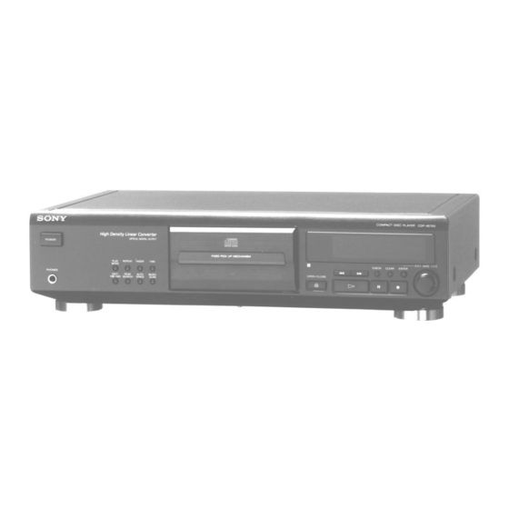
SERVICE MANUAL
Compact disc player
Laser
Semiconductor laser (λ = 780 nm)
Emission duration: continuous
Laser output
Max 44.6 µW*
* This output is the value measured at
a distance of 200 mm from the
objective lens surface on the Optical Pick-
up block with 7 mm aperture.
Frequency response
2 Hz to 20 kHz ± 0.5 dB
Signal-to-noise ratio
More than 102 dB
Dynamic range
More the 98 dB
Harmonic distortion
Less than 0.0035%
Channel separation
More than 100 dB
Outputs
Jack
Maximum
type
output
level
LINE OUT
Phono
2 V
jacks
(at 50 kilohms)
DIGITAL
Optical
–18 dBm
OUT
output
(OPTICAL)
connector
PHONES
Stereo
10 mW
phone
jack
MICROFILM
CDP-XE700
PHOTO : AEP model
Model Name Using Similar Mechanism
CD Mechanism Type
Base Unit Type
Optical Pick-up Type
SPECIFICATIONS
Load
impedance
Over 50 kilohms
Wave length : 660 nm
32 ohms
— 1 —
General
Power requirements
220 V – 230 V AC, 50/60 Hz
Power consumption
12W
430 × 1107 × 295 mm
Dimensions (approx.)
(17 × 4 1/4 × 11 5/8 in.) incl. projecting
(w/h/d)
parts
Mass (approx.)
3.6 kg (7 lbs 15 oz)
Supplied accessories
Audio cord (2 phono plugs–2 phono plugs) (1)
Remote commander (RM-D820) (1)
Sony SUM-3 (NS) batteries (2)
Design and specifications are subject to change without notice.
COMPACT DISC PLAYER
AEP Model
UK Model
CDP-XE800
CDM36-14
BU-14
KSS-213B/S-N
Advertisement
Table of Contents

Related Manuals for Sony CDP-XE700


Summary of Contents for Sony CDP-XE700
- Page 1 Frequency response 2 Hz to 20 kHz ± 0.5 dB Remote commander (RM-D820) (1) Signal-to-noise ratio More than 102 dB Sony SUM-3 (NS) batteries (2) Dynamic range More the 98 dB Harmonic distortion Less than 0.0035% Design and specifications are subject to change without notice.
-
Page 2: Table Of Contents
LINE WITH MARK ! ON THE SCHEMATIC DIAGRAMS AND IN THE PARTS LIST ARE CRITICAL TO SAFE OPERATION. REPLACE THESE COMPONENTS WITH SONY PARTS WHOSE PART NUMBERS APPEAR AS SHOWN IN THIS MANUAL OR IN SUPPLEMENTS PUBLISHED BY SONY. — 2 —... -
Page 3: Section 1. Servicing Note
SECTION 1 SERVICING NOTE HOW TO OPEN THE DISC TRAY WHEN POWER SWITCH NOTES ON HANDLING THE OPTICAL PICK-UP BLOCK TURNS OFF OR BASE UNIT The laser diode in the optical pick-up block may suffer Insert a screwdriver into the aperture of the unit bottom, and move it in the direction of arrow. -
Page 4: Section 2. General
SECTION 2 GENERAL LOCATION OF PARTS AND CONTROLS Front Panel 2 3 4 5 8 90 !¡!™ !• @º !ª !∞ !¢ !£ @™ @¡ !¶ !§ 1 POWER switch !£ ≠ AMS* ± knob 2 PLAY MODE button !¢ p (stop) button 3 REPEAT button !∞... -
Page 5: Section 3. Disassembly
SECTION 3 DISASSEMBLY Note : Follow the disassembly procedure in the numerical order given. 3-1. FRONT PANEL ASSEMBLY 1 Push the part A in the direction of arrow to remove the loading panel upward. A part 6 Two screws 8 Panel bracket (BVTP2.6x8) 4 Connector (CN751) -
Page 6: Section 4. Test Mode
SECTION 4 TEST MODE 4-1. AF MODE Button No. Button No. Button Button The following checks can be performed in the AF mode, which is set Displayed Displayed by connecting the TP2 (AFADJ) terminal on MAIN board to the TIME ENTER Ground and turning on the power. - Page 7 4-2. ADJ MODE [ MAIN BOARD ] — Component Side — The following operations are performed in the ADJ mode, which is set by connecting the TP1 (ADJ) terminal to the Ground and turning on the power. • During playback, there is no problem even if the GFS is continu- CN302 ously LOW.
-
Page 8: Section 5. Electrical Block Checking
SECTION 5 ELECTRICAL BLOCK CHECKING Note: Note: A clear RF signal waveform means that the shape “◊” can be clearly distinguished at the center of the waveform. 1. CD Block is basically designed to operate without adjustment. Therefore, check each item in order given. RF signal waveform 2. - Page 9 6. Check the level B of the oscilliscope's waveform and the A (DC RF PLL Free-run Frequency Check voltage) of the center of the Traverse waveform. Procedure : Confirm the following : 1. Connect frequency counter to test point (XPLCK) with lead wire. A/B x 100 = less than ±...
-
Page 10: Section 6. Diagrams
SECTION 6 DIAGRAMS 6-1. CIRCUIT BOARDS LOCATION POWER board BD board LOADING board HP board SPINDLE board KEY board MAIN board SLED board DISPLAY board — 10 —... -
Page 11: Ic Pin Function
6-2. IC PIN FUNCTION • IC801 SYSTEM CONTROL, FLUORESCENT INDICATOR TUBE DRIVE (CXP82316-069Q) Pin No. Pin Name Function TIMER – Connected to +5V. RM (BUSIN) Audio bus input. – Connected to +5V. OPEN – OPEN – Not used. (open) (BUS-OUT) –... -
Page 16: Front Panel Section
X-4946-575-1 PANEL ASSY (ALS), FRONT * 15 4-962-329-01 DAMPER (UK) 4-978-398-11 CUSHION (UK) 4-977-589-21 BUTTON (POWER) 4-978-398-21 CUSHION (AEP,G) 4-977-358-01 CUSHION (8X12.5) 4-963-404-21 EMBLEM (5-A), SONY 4-978-897-01 PLATE, INDICATION 4-951-620-01 SCREW (2.6X8), +BVTP X-3371-435-1 FOOT ASSY (F50150S) — 27 —... -
Page 17: Chassis Section
7-2. CHASSIS SECTION CD MECHANISM (CDM36-14) CNP901 (UK) not supplied CNP901 (AEP, G) T901 not supplied The components identified by mark ! or dotted line with mark not supplied ! are critical for safety. Replace only with part number specified. Ref. -
Page 18: Cd Mechanism Section (Cdm36-14)
7-3. CD MECHANISM SECTION (CDM36-14) BASE UNIT (BU-14) not supplied not supplied not supplied not supplied M151 not supplied not supplied not supplied not supplied Ref. No. Part No. Description Remark Ref. No. Part No. Description Remark 1-452-820-11 MAGNET (ASSY) 4-968-905-01 BELT (CDM) * 102 4-977-902-01 PANEL (DRAWER) -
Page 19: Base Unit Section (Bu-14)
7-4. BASE UNIT SECTION (BU-14) M101 not supplied M102 The components identified by mark ! or dotted line with mark ! are critical for safety. Replace only with part number specified. Ref. No. Part No. Description Remark Ref. No. Part No. Description Remark 4-977-925-01 SPRING(SLIDE BASE),COMPRESSION... -
Page 20: Section 8. Electrical Parts List
SECTION 8 ELECTRICAL PARTS LIST Note: • Due to standardization, replacements in the parts list • SEMICONDUCTORS The components identified by may be different from the parts specified in the dia- In each case, u: µ , for example: mark ! or dotted line with mark grams or the components used on the set. - Page 21 DISPLAY Ref. No. Part No. Description Remark Ref. No. Part No. Description Remark R127 1-216-049-91 METAL GLAZE 1/10W R184 1-216-065-00 METAL CHIP 4.7K 1/10W R131 1-216-037-00 METAL CHIP 1/10W (suffix-12) R133 1-216-073-00 METAL CHIP 1/10W R134 1-216-073-00 METAL CHIP 1/10W <...
- Page 22 DISPLAY LOADING MAIN Ref. No. Part No. Description Remark Ref. No. Part No. Description Remark R819 1-249-429-11 CARBON 1/4W R825 1-249-431-11 CARBON 1/4W R827 1-249-429-11 CARBON 1/4W R826 1-249-419-11 CARBON 1.5K 1/4W < SWITCH > < SWITCH > S801 1-554-303-21 SWITCH, TACTILE (ENTER) S820 1-554-303-21 SWITCH, TACTILE (TIME) S802...
- Page 23 MAIN Ref. No. Part No. Description Remark Ref. No. Part No. Description Remark C401 1-164-159-21 CERAMIC 0.1uF * CN302 1-568-839-11 SOCKET, CONNECTOR 23P C402 1-124-994-11 ELECT 100uF CN651 1-506-468-11 PIN, CONNECTOR 3P (AEP,G) CN951 1-766-269-11 PIN, CONNECTOR (PC BOARD) 7P C409 1-102-816-00 CERAMIC 120PF...
- Page 24 MAIN Ref. No. Part No. Description Remark Ref. No. Part No. Description Remark Q401 8-729-900-74 TRANSISTOR DTC143TS (AEP,G) R452 1-249-435-11 CARBON 1/4W Q401 8-729-141-30 TRANSISTOR 2SC3623A-LK (UK) (AEP,G) Q402 8-729-900-74 TRANSISTOR DTC143TS (AEP,G) Q404 8-729-029-56 TRANSISTOR DTA144ESA (AEP,G) R453 1-249-435-11 CARBON 1/4W (AEP,G) Q501...
- Page 25 CDP-XE700 SPINDLE MAIN POWER SLED Ref. No. Part No. Description Remark Ref. No. Part No. Description Remark R932 1-249-436-11 CARBON 1/4W MISCELLANEOUS *************** R933 1-247-807-31 CARBON 1/4W R934 1-249-421-11 CARBON 2.2K 1/4W 1-776-235-11 WIRE (FLAT TYPE) (23 CORE) R935 1-249-422-11 CARBON 2.7K...