Table of Contents
Advertisement
Quick Links
RX-V3200/DSP-AX3200
This manual has been provided for the use of authorized YAMAHA Retailers and their service personnel.
It has been assumed that basic service procedures inherent to the industry, and more specifically YAMAHA Products, are already
known and understood by the users, and have therefore not been restated.
WARNING:
IMPORTANT:
The data provided is believed to be accurate and applicable to the unit(s) indicated on the cover. The research, engineering, and
service departments of YAMAHA are continually striving to improve YAMAHA products. Modifications are, therefore, inevitable
and specifications are subject to change without notice or obligation to retrofit. Should any discrepancy appear to exist, please
contact the distributor's Service Division.
WARNING:
IMPORTANT:
I CONTENTS
TO SERVICE PERSONNEL .......................................... 1
IMPEDANCE SELECTOR ............................................. 1
SPECIFICATIONS ...................................................... 5~7
INTERNAL VIEW ........................................................... 8
DISASSEMBLY PROCEDURES ............................. 9~11
SELF DIAGNOSIS FUNCTION (DIAG) ................. 12~33
1 0 0 7 8 0
AV RECEIVER/AV AMPLIFIER
IMPORTANT NOTICE
Failure to follow appropriate service and safety procedures when servicing this product may result in personal
injury, destruction of expensive components, and failure of the product to perform as specified. For these reasons,
we advise all YAMAHA product owners that any service required should be performed by an authorized
YAMAHA Retailer or the appointed service representative.
The presentation or sale of this manual to any individual or firm does not constitute authorization, certification or
recognition of any applicable technical capabilities, or establish a principle-agent relationship of any form.
Static discharges can destroy expensive components. Discharge any static electricity your body may have
accumulated by grounding yourself to the ground buss in the unit (heavy gauge black wires connect to this buss).
Turn the unit OFF during disassembly and part replacement. Recheck all work before you apply power to the unit.
SERVICE MANUAL
AMP CHECK ................................................................ 34
DISPLAY DATA ..................................................... 35~36
IC DATA ................................................................. 37~43
BLOCK DIAGRAM ................................................. 44~47
PRINTED CIRCUIT BOARD .................................. 48~75
PIN CONNECTION DIAGRAM .............................. 76~77
SCHEMATIC DIAGRAM ........................................ 78~83
PARTS LIST ......................................................... 84~105
REMOTE CONTROL TRANSMITTER .............. 106~107
P.O.Box 1, Hamamatsu, Japan
Advertisement
Table of Contents

Related Manuals for Yamaha RX-V3200


Summary of Contents for Yamaha RX-V3200
-
Page 1: Table Of Contents
This manual has been provided for the use of authorized YAMAHA Retailers and their service personnel. It has been assumed that basic service procedures inherent to the industry, and more specifically YAMAHA Products, are already known and understood by the users, and have therefore not been restated. -
Page 2: To Service Personnel
RX-V3200/DSP-AX3200 I TO SERVICE PERSONNEL AC LEAKAGE WALL EQUIPMENT TESTER OR 1. Critical Components Information OUTLET UNDER TEST EQUIVALENT Components having special characteristics are marked s and must be replaced with parts having specifications equal to those originally installed. 2. Leakage Current Measurement (For 120V Models Only) -
Page 3: Front Panels
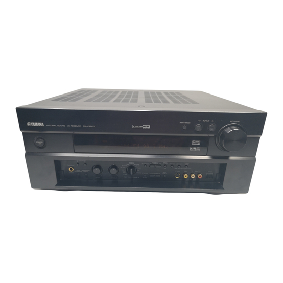
RX-V3200/DSP-AX3200 I FRONT PANELS RX-V3200 (U, C, A, R, T models) DSP-AX3200 (B, G models) I REAR PANELS RX-V3200 (U, C models) - Page 4 RX-V3200/DSP-AX3200 RX-V3200 (A model) RX-V3200 (R, T models) DSP-AX3200 (B model)
-
Page 5: Remote Control Transmitter
RX-V3200/DSP-AX3200 DSP-AX3200 (G model) I REMOTE CONTROL TRANSMITTER... -
Page 6: Specifications
Turnover Frequency ........... 3.5 kHz Finish Filter Characteristics RX-V3200 ........Gold color (U, C, R, T) models MAIN L/R, CENTER, Rear L/R/C Small (H.P.F.) .. 90 Hz, 12 dB/oct. Black color (U, C, R, A) models SUBWOOFER (L.P.F.) ........... 90 Hz, 18 dB/oct. - Page 7 RX-V3200/DSP-AX3200 U ..U.S.A. model C ..Canadian model A ..Australian model B ..British model G ..European model R ..General model T ..Chinese model Manufactured under license from Dolby Laboratories. “Dolby”, “Pro Logic” and the double-D symbol are trademarks of Dolby Laboratories.
- Page 8 RX-V3200/DSP-AX3200 • The variable range of the parameter (Min/Max/Step) Parameter name Pro Logic Pro Logic II Pro Logic II Neo:6 DD/dts/AAC 6.1/ES Unit Movie Music (P.) INIT. DLY 1/99/1 1/99/1 1/99/1 (P.) ROOM SIZE 0.1/2.0/0.1 0.1/2.0/0.1 0.1/2.0/0.1 (P.) LIVENESS 0/10/1...
- Page 9 H VIDEO (6) P.C.B. I VIDEO (1) P.C.B. J VIDEO (2) P.C.B. K VIDEO (4) P.C.B. L TUNER (RX-V3200 only) M MAIN (5) P.C.B. N MAIN (4) P.C.B. O POWER (4) P.C.B. P POWER (6) P.C.B. (R, T models only) Q MAIN (3) P.C.B.
-
Page 10: Disassembly Procedures
RX-V3200/DSP-AX3200 I DISASSEMBLY PROCEDURES Top Cover (Remove parts in the order as numbered.) Disconnect the power cord from the AC outlet. 1. Removal of Top Cover a. Remove 2 screws (1), 4 screws (2) and 2 screws (3). (Fig. 1) b. - Page 11 VIDEO (5) P.C.B. P.C.B.s and the Tuner* . (Fig. 5) (AAX30610) Rubber sheet : RX-V3200 only and cloth When checking the P.C.B.: • Put the rubber sheet and a cloth over the equipment. Then Tuner (RX- place the P.C.B. upside down on the cloth and check it. (Fig. 5) V3200 only) •...
- Page 12 RX-V3200/DSP-AX3200 9. Removal of VIDEO (6), VIDEO (7), and FUNCTION P.C.B.s a. Remove CB359, CB360, CB503, CB505, CB509 and CB936. (Fig. 6) b. Remove 10 screws (I). (Fig. 4) c. Remove VIDEO (6), VIDEO (7), and FUNCTION CB503 P.C.B.s. (Fig. 7) CB359 When checking the P.C.B.:...
-
Page 13: Self Diagnosis Function (Diag)
RX-V3200/DSP-AX3200 I SELF DIAGNOSIS FUNCTION (DIAG) There are 18 DIAG menu items, each of which has sub-menu items. Listed in the table below are menu items and sub-menu items. No DIAG menu sub-menu YSS938 1. ANALOG BYPASS 2. YSS 0dB 3. - Page 14 RX-V3200/DSP-AX3200 No DIAG menu sub-menu 14 IF STATUS 1. IS 1 2. IS 2 3. IS 3 4. CS 1 5. CS 2 6. CS 3 7. CS 4 8. CS 5 9. BY1 10. BY2 11. BY3 12. BY4 13.
- Page 15 RX-V3200/DSP-AX3200 • Starting DIAG Keys of main unit Press the “STANDBY/ON key while pressing those two keys indicated in the figure on [U, C, A, R, T models] PRESET/ the right. A/B/C/D/E TUNING • Starting DIAG in the protection cancel mode...
- Page 16 RX-V3200/DSP-AX3200 Cause: The voltage in the power supply section is abnormal. When there is a history of protection function due to Supplementary information: The abnormal voltage is displayed in % based on Version abnormal voltage in the 5V as 100%.
- Page 17 RX-V3200/DSP-AX3200 • Operation procedure of DIAG menu and SUB-MENU There are 18 MENU items, each of which has some SUB-MENU items. [U, C, A, R, T models] PRESET/ TUNING DIAG menu selection Main unit [U, C, A, R, T models]: Select the menu using...
- Page 18 RX-V3200/DSP-AX3200 • Details of DIAG menu With full-bit output specified in some modes, it is possible to execute 0dBFS output without head margin in each channel. 1. YSS938 This function is for YSS938 only. Main DSP of YSS938 is selected for MAIN L/R output.
- Page 19 RX-V3200/DSP-AX3200 YSS 0dB • The signal is output including the head margin. Head margin: Main L/R: 0dBFS, Center: -6dBFS, Rear Center: -3dBFS, FL/FR: -6dBFS, RL/RR: -12dBFS, SWFR: Add L/R signal at -20dBFS. Reference data (PRE OUT) INPUT: DVD ANALOG SWFR: 50Hz, Others: 1kHz...
- Page 20 RX-V3200/DSP-AX3200 2. YSS-CS 8 channels are made usable by CS49329. The signal enters YSS938 through the Sub DSP passage and then undergoes through-output. CS49329 is selected for the Main L/R output. Using the sub-menu, it is possible to select full bit output at 0dB output level.
- Page 21 RX-V3200/DSP-AX3200 3. CS-YSS 8 channels are made usable by CS49329. The signal enters YSS938 through the Sub DSP passage and then undergoes through-output. YSS938 Main DSP is selected for the Main L/R output. Using the sub-menu, it is possible to select full bit output at 0dB output level.
- Page 22 RX-V3200/DSP-AX3200 4. CS49329 8 channels are made usable by CS49329. The signal enters YSS938 through the Sub DSP passage and then undergoes through-output. CS49329 is selected for the Main L/R output. Using the sub-menu, it is possible to select full bit output at 0dB output level.
- Page 23 RX-V3200/DSP-AX3200 DSP THROUGH ~ CS (AAC/dts (ES auto)) CS49329 dts/AAC Analog RC/SW Sub DSP RC/SW Main DSP FL/FR Through Digital RL/RR RL/RR YSS938 5. HP ROUTE This function is for YSS938 only. Sub DSP SDOB3 of YSS938 is selected for MAIN L/R output.
- Page 24 RX-V3200/DSP-AX3200 6. RAM THROUGH This function is for YSS938 only. Main L/R signal is output through Main DSP of YSS938. CT/RC, RL/RR and FL/FR signals are output through Sub DSP - DRAM. Using the sub-menu, it is possible to select the full-bit output at 0dB output level.
- Page 25 RX-V3200/DSP-AX3200 7. DOLBY PRO LOGIC [YSS938] PRO LOGIC I Reference data (PRE OUT) INPUT: DVD ANALOG SWFR: 50Hz, Others: 1kHz Condition MAIN L/R CENTER REAR C SWFR RL/RR - ∞ - ∞ - ∞ - ∞ Each ch, -20 dBV, volume -10 dB -14.0 dBV...
- Page 26 RX-V3200/DSP-AX3200 Neo:6 Reference data (PRE OUT) INPUT: DVD ANALOG SWFR: 50Hz, Others: 1kHz Condition MAIN L/R CENTER REAR C SWFR RL/RR - ∞ - ∞ - ∞ - ∞ Each ch, -20 dBV, volume -10 dB -14.0 dBV - ∞...
- Page 27 RX-V3200/DSP-AX3200 8. SPEAKERS SET The input signal is automatically identified in the order of dts → DOLBY DIGITAL → AAC→ PCM → Analog. There are seven sub-menu items as follows. The signals output from the DSP block are the same as 1. YSS938: YSS 0dB.
- Page 28 RX-V3200/DSP-AX3200 9. DISPLAY CHECK This program is used to check the FL display section. The display condition varies as shown below according to the sub- menu operation. The signals are processed using EFFECT OFF (The L/R signal is output using ANALOG MAIN BYPASS.)
- Page 29 RX-V3200/DSP-AX3200 11. RS-232C This menu is used to check transmission of the data and the flow port of the hardware. With the power turned off, short between pins No.2 (RxD) and No.3 (TxD) and between pins No.7 (RTS) and No.8 (CTS) of the RS-232C terminal. (Be sure to RTS CTS turn off the power when shorting pins.)
- Page 30 RX-V3200/DSP-AX3200 13. AD DATA CHECK/FAN TEST This menu is used to display the A/D conversion value of the main CPU which detects panel keys of the main unit and protection functions in % using the sub-menu. (Reference voltage 5V as 100%) During signal processing, the condition before execution is maintained.
- Page 31 RX-V3200/DSP-AX3200 FAN DRIVE TEST HIGH FAN DRIVE TEST FAN DRIVE TEST 14. IF STATUS (Input function status) Using the sub-menu, the status data is displayed one after another in the hexadecimal notation. During signal processing, the status before execution of this menu is maintained.
- Page 32 RX-V3200/DSP-AX3200 <5th byte> Signal processing status information *2: With digital signals other than 32kHz, 44.1kHz and 48kHz, through processing method is used for reproducible signals. bit7 MUTE request bit3 – bit6 Red dts flashing bit2 Through & bypass (*2) bit5 6.1ch. field being processed bit1 –...
- Page 33 RX-V3200/DSP-AX3200 PLD/SRAM BUS CHECK Display Description WAIT Bus is being checked. NoEr No error detected. DATA Data bus shorted or open. (XX: 00-07) ADDR Address bus shorted or open. (XX: 00-0E) 16. CS DL CODE This menu is used to display the data version, TOC information and sum calculated value of the flash ROM for CS49329.
- Page 34 RX-V3200/DSP-AX3200 18. MICROPROCESSOR INFORMATION The version, checksum and the port specified by the microprocessor are displayed. The signal is processed using EFFECT OFF. The checksum is obtained by adding the data at every 16 bits for each program area and expressing the result as a 4-figure hexadecimal data.
-
Page 35: Amp Check
RX-V3200/DSP-AX3200 I AMP CHECK Confirmation of Idling Current 1) No signal applied. 2) Non-loaded condition. 3) Aging is 10 minutes Test Point Item Rating (DC) MAIN L Q58 Base – Emitter (MAIN [1] P.C.B.) Q65 Base – Emitter (MAIN [1] P.C.B.) MAIN R Q72 Base –... - Page 36 RX-V3200/DSP-AX3200 I DISPLAY DATA G V901 : 16-BT-91GK (V7683200) PATTERN AREA G PIN CONNECTION Pin No. Connection Pin No. Connection Note : 1) F1, F2 ..Filament 2) NP ..No pin 3) NC ..No connection (NC pin should be electrically open on the PC board.) 4) DL ..
- Page 37 RX-V3200/DSP-AX3200 G ANODE CONNECTION 13G~2G – – – – –...
- Page 38 RX-V3200/DSP-AX3200 I IC DATA IC514 : YSS938-F RAMA9 RAMA3 SELI1 RAMA4 SELI0 SELI9 SELOA SELI10 SELOB SELI11 TESTMS SELI12 TESTXEN SELI13 IPORT0 RAMA2 IPORT1 RAMA5 IPORT2 RAMA1 IPORT3 RAMA6 IPORT4 RAMA0 DDIN0 RAMA7 DDIN1 RAMA8 DDIN2 VDD1 DDIN3 RASN RAMOEN...
- Page 39 RX-V3200/DSP-AX3200 IC514 : YSS938-F Pin Description Name Function Crystal oscillator connecting terminal Crystal oscillator connecting terminal (24.576MHz ) SELI1 Built-in selector input 1 (AXD) SELI0 Built-in selector input 0 (GND) SELOA Built-in selector output A (ISEL) SELOB Built-in selector output B...
- Page 40 RX-V3200/DSP-AX3200 Name Function SDWCKI1 Word clock input terminal for SDIB, SDOB interface (Unconnected) SDBCKI1 Bit clock input terminal for SDIB, SDOB interface (Unconnected) Ground terminal SDOB3 PCM output terminal from Sub DSP SDOB2 PCM output terminal from Sub DSP SDOB1...
- Page 41 RX-V3200/DSP-AX3200 Name Function RAMA5 Sub DSP: External memory address terminal 5 RAMA2 Sub DSP: External memory address terminal 2 SELI13 Built-in selector input 13 (Unconnected) SELI12 Built-in selector input 12 SELI11 Built-in selector input 11 (Unconnected) SELI10 Built-in selector input 10 (Unconnected)
- Page 42 RX-V3200/DSP-AX3200 IC520 : M30802SGP 16bit µ-COM (Main CPU) /WRL/WR/CASL /WRH/BHE/CASH /RD/DW /BCLK/ALE/CLK M30802SGP /HLDA/ALE /HOLD /ALE/RAS /RDY /K13 /K12 /CYS /RTS /K11 /CLK /K10 /CTS /RTS /CTS /CLKS /CLK /SDA (*1) 0OUT /SCL (*1) N channnel Open Drain Output I/O Port...
- Page 43 RX-V3200/DSP-AX3200 IC520 : M30802SGP Pin Description Port No. Function name Detail of function Power ON Power OFF Backup TXDR 232C TX DATA / YDC TX DATA 232C RTS / YDC CLOCK 232C CTS DA/O FAN CONTROL SDTN NON AUDIO TX DATA...
- Page 44 RX-V3200/DSP-AX3200 Port No. Function name Detail of function Power ON Power OFF Backup EXT. ROM ADDRESS BUS KEEP EXT. ROM ADDRESS BUS KEEP EXT. ROM ADDRESS BUS KEEP EXT. ROM ADDRESS BUS KEEP EXT. ROM ADDRESS BUS KEEP EXT. ROM ADDRESS BUS KEEP EXT.
-
Page 45: Block Diagram
RX-V3200/DSP-AX3200 I BLOCK DIAGRAM (1/2) • See page E-78/J-72 → SCHEMATIC DIAGRAM XL503 • See page E-80/J-74 → SCHEMATIC DIAGRAM FUNCTION 24.576MHz IR REMOTE REMOTE JACK JK851, 852 U901 MICRO POWER RELAY DSP IC514 DIGITAL OUT COMPUTER MD/TAPE SPEAKER RELAY... - Page 46 RX-V3200/DSP-AX3200 I BLOCK DIAGRAM (2/2) • See page E-82/J-76 → SCHEMATIC DIAGRAM MAIN IC601 C-INPUT IC607 Q601, 604 SELECTOR 8ohm/4ohm S-MONITOR IC602 RY201 F202 SW1 (U, C, A, B, G, R, T models only) D-TV/LD Y-INPUT S-SIGNAL DETECTOR SELECTOR IC603...
-
Page 47: Printed Circuit Board
RX-V3200/DSP-AX3200 • Semiconductor Location I PRINTED CIRCUIT BOARD (Foil side) Circuit No. U, C R, T C517, 518, 533, 563, 564 C603, 604 Ref. No. Location Ref. No. Location Ref. No. Location Ref. No. Location Ref. No. Location C666, 671, 676, 678... - Page 48 RX-V3200/DSP-AX3200 • Semiconductor Location I PRINTED CIRCUIT BOARD (Foil side) Circuit No. U, C R, T C517, 518, 533, 563, 564 C603, 604 Ref. No. Location C666, 671, 676, 678 D502 D517, 518 J505, 506 D513 Q501, 502, 507, 508, 535, 536, 546, 547...
- Page 49 RX-V3200/DSP-AX3200 • Semiconductor Location I PRINTED CIRCUIT BOARD (Foil side) Ref. No. Location Ref. No. Location Ref. No. Location D801 IC803 Q902 D802 IC804 Q905 (Lead Type Device) OPERATION (1) P. C. B. D803 IC901 Q906 D804 Q801 Q907 From FUNCTION...
- Page 50 RX-V3200/DSP-AX3200 I PRINTED CIRCUIT BOARD (Foil side) (Lead Type Device) (Lead Type Device) OPERATION (4) P. C. B. OPERATION (6) P. C. B. From SET MENU – NEXT J, B, G models From From From U, C, A, R, T models only...
- Page 51 RX-V3200/DSP-AX3200 • Semiconductor Location I PRINTED CIRCUIT BOARD (Foil side) Ref. No. Location D508 D509 (Lead Type Device) DSP P. C. B. D510 D511 D512 From FUNCTION D513 D514 D515 IC501 IC502 IC503 IC508 To OPERATION (4) IC510 IC512 IC513...
- Page 52 RX-V3200/DSP-AX3200 • Semiconductor Location I PRINTED CIRCUIT BOARD (Foil side) Ref. No. Location D501 D502 D503 D504 D505 D506 D507 D516 D517 D518 D519 D520 (Surface Mount Device) DSP P. C. B. D521 D522 D523 D524 D525 D526 D527 D528...
- Page 53 RX-V3200/DSP-AX3200 • Semiconductor Location I PRINTED CIRCUIT BOARD (Foil side) Circuit No. U, C R, T B, G C653 IC606 Ref. No. Location Ref. No. Location J741, 742 D601 IC606 Q609 R674 D602 IC607 R675, 684 D603 IC608 R681 R682...
- Page 54 RX-V3200/DSP-AX3200 • Semiconductor Location I PRINTED CIRCUIT BOARD (Foil side) Circuit No. U, C R, T B, G C703, 711 Ref. No. Location C758~770 CB752~754 D751 D751, 752 D752 IC704 IC754~756 IC701 JB41 R711, 712 IC702 (Lead Type Device) (Lead Type Device) VIDEO (2) P.
- Page 55 RX-V3200/DSP-AX3200 • Semiconductor Location I PRINTED CIRCUIT BOARD (Foil side) Circuit No. U, C R, T B, G CB582 Ref. No. Location R583 R584 D581 R585 R586 Q582 (Lead Type Device) VIDEO (5) P. C. B. R859 X: NOT USED...
- Page 56 RX-V3200/DSP-AX3200 I PRINTED CIRCUIT BOARD (Foil side) (Lead Type Device) (Surface Mount Device) (Lead Type Device) VIDEO (6) P. C. B. VIDEO (6) P. C. B. VIDEO (7) P. C. B. From From FUNCTION FUNCTION FREQUENCY STEP (R, T models only)
- Page 57 RX-V3200/DSP-AX3200 • Semiconductor Location I PRINTED CIRCUIT BOARD (Foil side) Ref. No. Location Ref. No. Location Ref. No. Location Ref. No. Location Ref. No. Location Ref. No. Location Ref. No. Location Ref. No. Location Ref. No. Location Ref. No. Location Ref.
- Page 58 RX-V3200/DSP-AX3200 I PRINTED CIRCUIT BOARD (Foil side) MAIN (4) P. C. B. (Lead Type Device) (Lead Type Device) (Lead Type Device) MAIN (2) P. C. B. MAIN (3) P. C. B. MAIN A REAR U, C, A, B, G, R, T models –...
- Page 59 RX-V3200/DSP-AX3200 • Semiconductor Location I PRINTED CIRCUIT BOARD (Foil side) Ref. No. Location D311 D312 From FUNCTION To MAIN (1) POWER (1) P. C. B. D313 To FUNCTION D314 (Lead Type Device) D315 D351 From Power Transformer D352 OPERATION (1)
- Page 60 RX-V3200/DSP-AX3200 • Semiconductor Location I PRINTED CIRCUIT BOARD (Foil side) Circuit No. U, C R, T C438, 439 Ref. No. Location D353 D431 D431 J311 JK431~433 IC431 (Lead Type Device) POWER (3) P. C. B. R366 SW311, 314, 318, 321...
-
Page 61: Pin Connection Diagram
RX-V3200/DSP-AX3200 I PIN CONNECTION DIAGRAM • ICs µPC29M33T-E1 LM61CIZ NJM7805FA NJM79M05FA PQ025EZ5MZP NJM7812FA NJM79M12FA NJM78M05FA 3: IN 3: +Vs 3: IN 3: COM 2: COM 1: OUT 1: OUT 2: Vout 1: OUT 1: GND 2: COM 2: IN µPC4570HA... - Page 62 RX-V3200/DSP-AX3200 • Diodes 1SR139 MTZJ4.7C 1SS355 1SS133 MTZJ9.1A 1SS380 Anode HZS7B2TD MTZJ11.0B MA8051-M Anode MA185 MTZJ12.0A MA8056-M MTZJ12.0B MA8062-H MTZJ15.0B RB501V-40 Cathode MTZJ18.0C UDZS5.6BTE-17 Cathode MTZJ22.0B MTZJ24.0B MTZJ24.0C MTZJ33.0D D3SBA20 S1NB20 D15XB20 – – • Transistors 2SA893A 2SC1740S 2SA1837 2SC5358...
- Page 63 RX-V3200/DSP-AX3200 SCHEMATIC DIAGRAM (FUNCTION) E-79/J-73 E-80/J-74 To OPE (2) E-79/J-73 Point 1 emitter of Q511 Point 2 Pin 20 of IC520 and collector of Q512 INPUT SELECTOR MUTE A Q511 E DIGITAL IN ELECTRIC VOLUME B Q512 C 11.7 11.8 -11.8...
- Page 64 RX-V3200/DSP-AX3200 SCHEMATIC DIAGRAM (OPERATION) IC802: NJM2068L-D IC803: µPC4570HA Dual OP-Amp Dual OP-Amp 10.1 FRONT L 11.8 PHONES 11.8 MUTE Vcc Vo PHONES IC804: NJM4556AL Dual OP-Amp 2, 6 OUTPUT -8.5 –INPUT 1, 7 +INPUT 3, 5 -9.5 -11.8 V– -11.8 -10.1...
- Page 65 RX-V3200/DSP-AX3200 SCHEMATIC DIAGRAM (DSP) to OPERATION (4) E-79/J-73 E-78/J-72 IC501, 502: TC74HCU04AF IC503: TC74HCT00AF IC509, 518~523: µPC4570G2 Hex Inverters Quad 2-Input Nand Gate Dual OP-Amp # All voltages are measured with a 10MΩ /V DC electric volt meter. # Components having special characteristics are marked s and must be...
- Page 66 RX-V3200/DSP-AX3200 SCHEMATIC DIAGRAM (VIDEO) Point 4 Pin 3 of IC610 IC601: TK15420M IC602~605: MM74HC4051N Video Amp IC702, 703: MM74HC4051SJX 8-Channel Analog Multiplexer IN/OUT OUT A –IN A OUT B – – +IN A –IN B +IN B COMMON OUT/IN Logic Binary to 1 -4.9...
- Page 67 RX-V3200/DSP-AX3200 SCHEMATIC DIAGRAM (MAIN) to POWER (1) E-83/J-77 POWER AMP (L ch) 61.6 61.6 60.5 60.4 60.5 59.9 RELAY 59.9 61.2 61.6 DRIVER 59.9 59.9 61.6 FRONT L 59.9 59.9 -0.5 -0.1 -1.1 60.7 59.9 18.0 18.0 18.0 -0.6 POWER SUPPLY -0.6...
- Page 68 RX-V3200/DSP-AX3200 SCHEMATIC DIAGRAM (POWER) FRONT L TO MAIN (1) E-82/J-76 IC351~353: NJM7805FA to POWER (3) IC355: NJM7812FA IC: NJM78M12FA Voltage Regulator INPUT OUTPUT 12.1 18.0 -0.1 -19.0 AC 28.8 18.0 CENTER -0.1 COMMON -12.1 RS-232C -19.0 REAR L DRIVER/ RECEIVER...
-
Page 69: Parts List
RX-V3200/DSP-AX3200 I WARNING PARTS LIST Components having special characteristics are marked s and must be replaced with parts having specifications equal to those originally in- stalled. I ELECTRICAL PARTS Carbon resistors (1/6W or 1/4W) are not included in the ELECTRICAL PARTS List. - Page 70 RX-V3200/DSP-AX3200 P.C.B. FUNCTION Schm Schm Ref. PART NO. Description Markets Ref. PART NO. Description Markets V8201100 P.C.B. FUNCTION C550 UU147100 C.EL 10uF V8201200 P.C.B. FUNCTION C551 UR865220 C.EL 0.22uF V8201300 P.C.B. FUNCTION C552 UU147100 C.EL 10uF V8201400 P.C.B. FUNCTION C553 UU147100 C.EL...
- Page 71 RX-V3200/DSP-AX3200 P.C.B. FUNCTION Schm Schm Ref. PART NO. Description Markets Ref. PART NO. Description Markets C612 UP652470 C.POL 470pF 100V C676 US135100 C.CE.CHP 0.1uF UCABG C613 UP652470 C.POL 470pF 100V C677 US063100 C.CE.M.CHP 1000pF C614 UP652470 C.POL 470pF 100V C678 US135100 C.CE.CHP...
- Page 72 RX-V3200/DSP-AX3200 P.C.B. FUNCTION & P.C.B. OPERATION Schm Schm Ref. PART NO. Description Markets Ref. PART NO. Description Markets PJ503 V4198900 JACK.PIN V8202600 P.C.B. OPERATION PJ504 V4199200 JACK.PIN V8202700 P.C.B. OPERATION UCRTA PN501 V3750200 L=70 CB801 VF982300 CN.BS.PIN Q501 VD303700 2SC3326 A,B...
- Page 73 RX-V3200/DSP-AX3200 P.C.B. OPERATION & P.C.B. DSP Schm Schm Ref. PART NO. Description Markets Ref. PART NO. Description Markets C910 UU118330 C.EL 330uF 6.3V ST891 BB071360 SCR.TERM 8.3x13 C911 VJ599100 C.CE.TUBLR 0.1uF ST901 VP750600 SCR.TERM MEP1700 C912 VJ599100 C.CE.TUBLR 0.1uF ST935 BB071360 SCR.TERM...
- Page 74 RX-V3200/DSP-AX3200 P.C.B. DSP Schm Schm Ref. PART NO. Description Markets Ref. PART NO. Description Markets C528 US135100 C.CE.CHP 0.1uF C597 US135100 C.CE.CHP 0.1uF C529 US135100 C.CE.CHP 0.1uF C598 US061470 C.CE.M.CHP 47pF C530 US135100 C.CE.CHP 0.1uF C599 US061470 C.CE.M.CHP 47pF C531 UR819100 C.EL...
- Page 75 RX-V3200/DSP-AX3200 P.C.B. DSP Schm Schm Ref. PART NO. Description Markets Ref. PART NO. Description Markets C660 Vi715100 C.MYLAR 470pF C732 UR819100 C.EL 1000uF 6.3V C661 Vi715100 C.MYLAR 470pF C733 US135100 C.CE.CHP 0.1uF C662 Vi715100 C.MYLAR 470pF C734 US062100 C.CE.M.CHP 100pF...
- Page 76 RX-V3200/DSP-AX3200 P.C.B. DSP & P.C.B. VIDEO Schm Schm Ref. PART NO. Description Markets Ref. PART NO. Description Markets L501 V2726500 COIL 68uH CB590 V7825500 5P TE TUC SERIES L502 V2726500 COIL 68uH CB591 V7826000 10P TE TUC SERIES L503 V2726500...
- Page 77 RX-V3200/DSP-AX3200 P.C.B. VIDEO Schm Schm Ref. PART NO. Description Markets Ref. PART NO. Description Markets C622 UR837470 C.EL 47uF D610 VT332900 DIODE 1SS355 C623 UR837470 C.EL 47uF D751 VT332900 DIODE 1SS355 C624 UR837470 C.EL 47uF D752 VT332900 DIODE 1SS355 C625 UM397100 C.EL...
- Page 78 RX-V3200/DSP-AX3200 P.C.B. VIDEO & P.C.B. MAIN Schm Schm Ref. PART NO. Description Markets Ref. PART NO. Description Markets R686 HV755470 R.CAR.FP 470Ω 1/4W UU138100 C.EL 100uF R688 HV753470 R.CAR.FP 4.7Ω 1/4W UU166470 C.EL 4.7uF R716 HV755270 R.CAR.FP 270Ω 1/4W UU165100 C.EL...
- Page 79 RX-V3200/DSP-AX3200 P.C.B. MAIN Schm Schm Ref. PART NO. Description Markets Ref. PART NO. Description Markets C105 UU167100 C.EL 10uF C166 UA654100 C.MYLAR 0.01uF C106 VK533900 C.PP 100pF 200V iF004600 DIODE 1SS133 C107 UU148100 C.EL 100uF iF004600 DIODE 1SS133 C108 UU166330 C.EL...
- Page 80 RX-V3200/DSP-AX3200 P.C.B. MAIN Schm Schm Ref. PART NO. Description Markets Ref. PART NO. Description Markets VC398400 DIODE MA185 s Q39 iA1015I0 2SA1015 Y VC398400 DIODE MA185 s Q40 VE198700 2SA1145 O,Y VC398400 DIODE MA185 s Q41 iC224030 2SC2240 GR,BL VC398400...
- Page 81 RX-V3200/DSP-AX3200 P.C.B. MAIN & P.C.B. POWER Schm Schm Ref. PART NO. Description Markets Ref. PART NO. Description Markets s R5 HV755150 R.CAR.FP 150Ω 1/4W s R169 HV753470 R.CAR.FP 4.7Ω 1/4W s R7 HV754100 R.CAR.FP 10Ω 1/4W s R170 HV755470 R.CAR.FP 470Ω...
- Page 82 RX-V3200/DSP-AX3200 P.C.B. MAIN & P.C.B. POWER Schm Schm Ref. PART NO. Description Markets Ref. PART NO. Description Markets s R262 HV754100 R.CAR.FP 10Ω 1/4W C354 UR759100 C.EL 1000uF s R265 HV753100 R.CAR.FP 1Ω 1/4W C355 VJ599100 C.CE.TUBLR 0.1uF R266 HV756330 R.CAR.FP...
- Page 83 RX-V3200/DSP-AX3200 P.C.B. POWER & Chip Resistors Schm Schm Ref. PART NO. Description Markets Ref. PART NO. Description Markets IC357 X0515A00 LM61CIZ THERMAL RD350000 R.CAR.CHP 0Ω 1/10W IC431 XW863A00 ADM202JRN-REEL7 RD353220 R.CAR.CHP 2.2Ω 1/10W JK431 VJ726800 JACK.MNI UCRTA RD354330 R.CAR.CHP 33Ω...
- Page 84 RX-V3200/DSP-AX3200 IEXPLODED VIEW U,C,G version R,T version 4-10 R,T version 4-10 4-10 4-12 2-21 R,T version 2-26 2-21 200-2 2-20 16 (4) 2-21 200-1 16 (2) 2-21 2-14 12 (1) 2-21 5-13 2-19 16 (1) 2-13 2-22 14 (4) 14 (5)
- Page 85 RX-V3200/DSP-AX3200 I MECHANICAL PARTS Ref. PART NO. Description Remarks Markets V7678900 FRONT PANEL RXV3200GD V7678800 FRONT PANEL RXV3200BL V7679100 FRONT PANEL DSPAX3200BL V7679300 FRONT PANEL DSPAX3200TI V6003900 ESCUTCHEON/POWER V6003800 ESCUTCHEON/POWER V6004000 ESCUTCHEON/POWER V6004200 ESCUTCHEON/INPUT V6004100 ESCUTCHEON/INPUT V6004300 ESCUTCHEON/INPUT V6004900 EMBLEM...
- Page 86 RX-V3200/DSP-AX3200 Ref. PART NO. Description Remarks Markets 2-14 V7992500 BUTTON/POWER 2-14 V7992400 BUTTON/POWER 2-14 V7992600 BUTTON/POWER 2-19 V6071000 SUPPORT SHAFT 2-20 V8622800 EARTH PLATE 2-21 EP600190 BIND HEAD B-TITE SCREW MFZN2BL 2-22 EP600130 BIND HEAD B-TITE SCREW MFZN2Y 2-23 VN413300 BIND HEAD BONDING B-T.
- Page 87 RX-V3200/DSP-AX3200 Ref. PART NO. Description Remarks Markets MF113160 FLEXIBLE FLAT CABLE 13P 160mm P=1.25 V8227900 S FLEXIBLE FLAT CABLE 15P 250mm P=1.25 MF111100 FLEXIBLE FLAT CABLE 11P 100mm MF117200 FLEXIBLE FLAT CABLE 17P 200mm MF115100 FLEXIBLE FLAT CABLE C&C 15P 100mm...
- Page 88 RX-V3200/DSP-AX3200 Ref. PART NO. Description Remarks Markets VK522000 SPECIAL SCREW S-TITE 4x8-10 MFC2BL VK522100 SPECIAL SCREW S-TITE 4x8-10 MFC2BL VY980100 PLATE, FAN COVER VQ199500 DAMPER TRANSF VK173200 SCREW, TRANSISTOR 3x15 SP MFC2 V6983800 SPACER/T05 VQ758300 CUSHION, L V6276700 CUSHION, FCB...
- Page 89 RX-V3200/DSP-AX3200 Parts List for Carbon Resistors Value 1/4W Type Part No. 1/6W Type Part No. Value 1/4W Type Part No. 1/6W Type Part No. 1.0 Ω 3100 3100 10 kΩ 7100 7100 HJ35 HF85 HF45 HF45 1.8 Ω ❊ 3180 11 kΩ...
-
Page 90: Remote Control Transmitter
RX-V3200/DSP-AX3200 I REMOTE CONTROL TRANSMITTER G SCHEMATIC DIAGRAM... - Page 91 RX-V3200/DSP-AX3200 Initial Code Zone2 Key Name *1; These code are transmitted when "DSP" is set-up as AMP library. –– –– –– –– *2; These code are transmitted when "ZONE2" is chosen RE-NAME –– –– –– with Select key. CLEAR ––...
- Page 92 RX-V3200/DSP-AX3200...