Table of Contents
Advertisement
NOTES
*
As for this model, the tuner of the DSP type is used.
When you exchange it due to the tuner pack(BL101;880-
2091M) trouble, it is necessary to adjust for S-meter etc.
Special JIG is necessary for an accurate adjustment. The
procedure document for the exclusive use jig is appended
to it.
*
This system controller IC M30876FJBGP(IC402) of Main
PWB does not have program. Please use special JIG at
the time of IC ex-change to write the memory.
*
This DSP IC SAF7730HV/N317(IC301) of Main PWB is
exposed die soldering pad type. It cannot remove in an
ordinary soldering iron.
Please use special removal JIG at the time of IC ex-
change
*
The
word mark and logos are owned by the
Bluetooth SIG, Inc. and any use of suchmarks by
CLARION CO.,LTD. is under license.
*
We cannot supply PWB with component parts in prin-
ciple. When a circuit on PWB has failure, please repair it
by component parts base. Parts which are not mentioned
in service manual are not supplied.
*
Specifications and design are subject to change without
notice for further improvement.
SPECIFICATIONS
Radio section
Tuning system:
PLL Frequeency synthesizer sys-
tem
Clarion Co., Ltd.
7-2, Shintoshin, Chuo-ku, Saitama-shi, Saitama 330-0081 Japan
Service Dept.: 7-2, Shintoshin, Chuo-ku, Saitama-shi, Saitama 330-0081 Japan
Tel: +81-48-601-3705 FAX: +81-48-601-3804
Service Manual
- 1 -
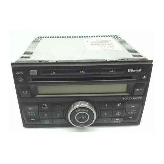
NISSAN Automobile Genuine
6CD LW/MW/FM/RDS Bluetooth
Combination
PN-3124N-A
Model
(Genuine No.28184 EB46A)
PN-3124N-B
Model
(Genuine No.28184 EB46B)
Receive range:
LW
MW
FM
Intermediate frequency:
LW/MW/FM
Quieting sensitivity:
LW
MW
FM
Separation:
FM
S/N ratio:
LW
MW
FM
Auto tuning stop sensitivity:
LW/MW
FM
CD section
Disc:
12cm disc
Separation:
More than 50dB
(20kHz L.P.F)
S/N ratio:
More than 74dB(20kHz L.P.F. JIS-A)
Distortion:
Less than 0.2%(20kHz L.P.F.)
General
Load impedance:
4ohm/CH
Power output:
40W x4
Power supply voltage: DC13.2V(10.8 to 15.6V)
Negative ground
Back-up consumption: Less than 0.5mA
Dimensions(mm):
178(W) x 100(H) x 164(D)
Weight:
2.3kg
Published by Service Dept.
298-6547-00 Mar.2008 X
Printed in P.R.C
153kHz to 279kHz
531kHz to 1,602kHz
87.5MHz to 108.0MHz
10.7MHz
Less than 45dBu
(at 20dB S/N)
Less than 37dBu
(at 20dB S/N)
Less than 15dBu
(at 30dB S/N)
22+5/-7dB(1kHz)
More than 40dB
More than 40dB
More than 50dB
47+6/-6dBu
29+6/-6dBu
PN-3124N
Advertisement
Table of Contents

Related Manuals for Clarion PN-3124N-A


Summary of Contents for Clarion PN-3124N-A
- Page 1 LW/MW word mark and logos are owned by the 47+6/-6dBu Bluetooth SIG, Inc. and any use of suchmarks by 29+6/-6dBu CLARION CO.,LTD. is under license. CD section We cannot supply PWB with component parts in prin- Disc: 12cm disc ciple. When a circuit on PWB has failure, please repair it...
- Page 2 TYPE sistors, etc). DESIGN NOTE No. Please make an operation test after replacement. Bluetooth ID Clarion co., Ltd MADE IN 8. Cautions in handling flexible PWB 276- PART NO. Before working with a soldering iron, make sure that the iron tip temperature is around 270 .
- Page 3 EXPLANATION OF IC 051-3518-90 NJM2846DL3-33-TE1 Positive Voltage Regurator 3.3V 051-3516-90 S-1132B33-U5T1G Positive Voltage Regurator 3.3V Power Outut Ground Vout Ground Ground Control in, H = ON. No Connectin Control (H= On) 051-3517-90 impossible of exchange (LT3481EMSE#TRPBF) 051-3519-90 NJU7771F05-TE2 Step-Down Switching Regulator Positive Voltage Regurator 5.0V TOP V I E W Control (H= On)
- Page 4 pin 16: ACC IN : IN : ACC ON flag input. pin 72: RDS CL 1 : IN : RDS 1 serial clock output. pin 17: PLL DO : O : PLL serial data output. pin 73: RDS DA 1 : IN : RDS 1 serial data input.
- Page 5 1/2SYS 9V SYS 9V Q110,111 SPEED SIGNAL ANT-ON SYS5V IMMOBI I/F IMMOBILIZER BT 3.3V SYS 5V VDD 5V Q518,519 REG IC505 IC502 ( PN-3124N-A ) J502 AUDIO-CPU DSP-3.3V TUNER 5V SYS 12V BACK UP TUNER 9V Main Connector IC504 IC104 Q109 Q516,517...
- Page 6 TROUBLESHOOTING Power on No power No sound CD Confirm to Check circuit line of B/U5V, ACC, Check Confirm to B/U, ACC SYS5V the voltage value of the display the voltage value of Q515, IC801 IC505, Q520, Q519 Confirm to Check Check the voltage value of the display...
- Page 7 The cellular phone and Bluetooth cannot be connected. Check enter in a set screen of the telephone Confirm to Check IC901 (Bluetooth module) the power of IC901 (Bluetooth module) IC502 (the power of 3.3V) Confirm to IC901 (Bluetooth module) the circuit of Q101,102,104,105,106,107,108 Confirm to Check...
- Page 8 EXPLODED VIEW/PARTS LIST 49 50 PN-3124N - 8 -...
- Page 9 310-1823-10 UPPER CASE 074-1237-69 OUTLET SOCKET (19P) 735-2614-1B MACHINE SCREW (M2.6 x 14) 076-0478-59 PLUG (9P) 714-2606-8B MACHINE SCREW (M2.6 x 6) 10 076-3011-72 PLUG (22P) 276-0034-75 SET PLATE (PN-3124N-A) 076-3011-66 PLUG (16P) 276-0034-76 SET PLATE (PN-3124N-B) 880-2091M TUNER PACK 060-8062-50 CERAMIC-ANT...
- Page 10 ELECTRICAL PARTS LIST Switch PWB(B1) section REF No. PART No. DESCRIPTION REF No. PART No. DESCRIPTION REF No. PART No. DESCRIPTION ANT902 060-8062-50 CERAMIC-ANT D835 001-7093-91 RFY1112H-16-TR R802 119-3331-15 1/10W 33k ohm C802 168-1042-78 16V 0.1uF R803 119-1021-15 1/10W 1k ohm C803 168-1042-78 16V 0.1uF D836...
- Page 11 C316 168-1022-55 1000pF K C534 168-5632-78 16V 0.056uF C104 168-2222-55 2200pF K C317 166-1011-50 100pF CH C535 168-5632-78 16V 0.056uF (PN-3124N-A) C318 168-1042-78 16V 0.1uF C536 168-5632-78 16V 0.056uF C108 166-1511-50 150pF CH C319 168-5622-55 5600pF K C537 178-1052-78 1uF...
- Page 12 119-1011-15 1/10W 100 ohm Q108 125-2027-91 DTC114EUA R148 116-1091-15 1/4W 1 ohm R345 119-1011-15 1/10W 100 ohm Q109 192-5886-00 2SC5886 (PN-3124N-A) R346 119-0000-05 1/10W 0 ohm JW Q110 125-2027-90 DTC143EU R149 116-1221-15 1/4W 1.2k ohm R347 119-0000-05 1/10W 0 ohm JW...
- Page 13 REF No. PART No. DESCRIPTION REF No. PART No. DESCRIPTION REF No. PART No. DESCRIPTION R406 119-1021-15 1/10W 1k ohm R471 119-1241-15 1/10W 120k ohm R568 116-1221-15 1/4W 1.2k ohm R407 119-1021-15 1/10W 1k ohm R472 119-3331-15 1/10W 33k ohm R569 116-1221-15 1/4W 1.2k ohm R408...
- Page 14 PRINTED WIRING BOARD Switch PWB(B1) section D813 D812 D810 D809 D807 D806 D808 S811 S821 D811 S816 S804 S803 D815 D861 S802 S825 LCD801 D862 D816 S807 S810 S801 D818 D857 D839 D814 CERAMIC ANT902 S823 D817 D838 D858 S812 S815 COMPONENT SIDE Caution:...
- Page 15 CIRCUIT DIAGRAM Switch PWB(B1) section LCD801 379-1392-52 J801 074-3013-72 P402 FL-GND MINI-J-ON ILL-(USA) 13.0V ILL+ 6CD SLOT+B 8.9V BL+B 4.9V CD-EJ CD-EJ 4.9V LOAD LOAD 4.9V POW-SW 3.3V POW-SW To page 21 D-GND (DISP-SW) P402 of 9.0V LCD+B Main PWB 4/5 5.0V SYS+5V LCD-BACK-LIGHT...
- Page 16 MIC SIGNAL ACTIVE ANT L108 : USED ANTENNA BOOST N.C. MIC GND TM501 R584 TM102 C554 C141 R248 AMP TYPE N.C. MIC VCC ( PN-3124N-A ) Q111 N.C. N.C. C229 Q220 C556 PASSIVE ANT C574 N.C. Q220 N.C. D510 R151 Q219...
- Page 17 ACTIVE ANT N.C. MIC SIGNAL : USED ANTENNA BOOST 1 2 3 4 5 6 7 8 9 N.C. MIC GND AMP TYPE N.C. MIC VCC ( PN-3124N-A ) N.C. N.C. PASSIVE ANT N.C. N.C. ( PN-3124N-B ) C517 N.C. R519 N.C.
- Page 18 Main PWB(B2) section 1/5 BL101 880-2091M ACTIVE ANT TUNER : USED ANTENNA BOOST ANT101 150P AMP TYPE GT13-SHA ( PN-3124N-A) ANTENNA ON ACTIVE ANT PASSIVE ANT : USED ANTENNA BOOST ( PN-3124N-B) AMP TYPE 11 12 14 15 ( PN-3124N-A...
- Page 19 Main PWB(B2) section 2/5 J201 R248 TH12 TH201 Q220 074-1302-12 0.285A 2SB1197 5.0V 1/4W 5.0V N.C. MIC SIGNAL N.C. MIC GND N.C. MIC VCC N.C. N.C. MIC+B N-BUS-SIG-IN N.C. N.C. 4.7K N.C. N.C. C241 C242 C204 1000p 1000p A/C-L+ C203 A/C-L- MIC-SIG To page 18...
- Page 20 Main PWB(B2) section 3/5 D+1.8 MEM+1.8 20kHz-LPF R356 D+3.3 R355 To page 22 R354 R353 TUNER To page 18, 22 A-GND 1/5, 5/5 RDS-DEC-I/F AGC12 BCK-IN4 R352 M LSB 1.1V 2.5V 2.5V ADSP-IOF6 AGC21 FR/RR-LIM C343 1000p M MSB ADSP-IOF5 AGC22 CLI-CLA-CNT 3.3V...
- Page 21 Main PWB(B2) section 4/5 To page 20 DSP-CPU SYS+5V SYS+5V POW-CPU CD-CPU SYS-ACC IMMOBI RDS-CL1 To page 22 RDS-DA1 B/U+5V B/U+5V L402 ILL+ 2.2uH To page 19 ILL- LCD+B B/T RESETP B/L+B 6CD SLOT+B P402 B/U-DET CCT401 076-3011-72 J801 1Kx4 FL-GND MINI-J-ON ILL-...
- Page 22 Main PWB(B2) section 5/5 1 N.C. FRONT-RH(+) FRONT-LH(+) FRONT-RH(-) FRONT-LH(-) REAR-RH(+) REAR-LH(+) REAR-RH(-) ILL-FIL ACC-FIL REAR-LH(-) STRG GND 20K-LPF 9.0V IC503 STRG SW A STRG SW B TA8275 PRE-AMP IMMOBILIZER N.C. SPEED SIGNAL C504 R505 R525 ILLUMI (+) BACK UP 10 11 12 13 14 15 16 17 18 19 20 21 22 23 24 25 R584...
- Page 23 Clarion Co., Ltd. Published by Service Dept. 7-2, Shintoshin, Chuo-ku, Saitama-shi, Saitama 330-0081 Japan Mar.2008 Service Dept.: 7-2, Shintoshin, Chuo-ku, Saitama-shi, Saitama 330-0081 Japan Printed in P.R.C Tel: +81-48-601-3705 FAX: +81-48-601-3804 Service Manual In Dash 6disk CD Auto Changer Mechanism (GI-X)
- Page 24 pin 70: AWRC : O : Control signal output for the active wide pin 22: FL RX : IN : Serial data input for the flash memory. range VCO. pin 23: LED SW : O : Mechanism sensor LED Drive control. pin 71: P VDD : - : PLL positive voltage supply.
- Page 25 pin 79: TEST 1 : IN : For the test. pin 80: TEST 2 : IN : For the test. pin 81: TEST 3 : IN : For the test. pin 82: TEST 4 : IN : For the test. pin 83: I2C REQUEST : O : I2C request output.
- Page 26 DISASSEMBLY How to remove "DISCHOLDER UNIT" How to remove "CD-PWB-ASSY" 1. Remove eight screws. 1. Add +5V to "U+" terminal of UD-MOTOR-ASSY,then 2. Remove the FPC. SIDE-P-ASSY-F moves outside of CD-PWB. 2. Release four FPCs. 3. Remove three screws 4. Remove the washer. 5.
- Page 27 How to remove "C-DRIVE UNIT" How to remove "LO-MOTOR-S-ASSY" 1. Remove the screw and DRIVE SPRING-A. 1. Remove two screws and DRIVE CHASSIS-B. 2. Rotate C-DRIVE UNIT internally. 2. Remove the screw of the bottom side. 3. Remove the washer, and remove C-DRIVE UNIT. 3.
- Page 28 OPERATION Discholder MOT2 (Mode Motor) S1 of CD-PWB (Mode Plate) S2 of CD-PWB (Mode Plate) Drive Unit S3 of CD-PWB (Mode Plate) MOT3 (UP/DW-Motor) S5 of SENSOR-U-FPC (Sutter) MOT1 (Loading Motor) S4 of CD-PWB (Holder) Loading Roller Shutter PT3 of SENSOR-L-FPC PT2 of SENSOR-L-FPC PT1 of SENSOR-L-FPC IC10 of CD PWB...
- Page 29 EXPLODED VIEW/PARTS LIST Main section to A1 to C2 to C4 to C3 to B1 to B2 to C1 to A6 to A7 to A3 23 16 to A5 to A2 to A4 to D2 to E1 33 34 to D3 * Do not reuse the following parts.
- Page 30 Lower unit assy section to A1 to A2 to A3 to A5 to A7 to A6 PART NO. DESCRIPTION Q'TY PART NO. DESCRIPTION Q'TY 966-1869-20 LOWER-C-ASSY 620-1624-24 GEAR COVER 966-0658-22 DH-SP-ASSY A 621-0732-21 M-GEAR B 966-1758-20 DS-SP-ASSY A 621-0733-20 M-GEAR C 966-1808-20 DH-SP-ASSY S 716-1850-01 SCREW(M2.0x2.0) 966-1809-20 DH-SP-ASSY R...
- Page 31 [Grease Point] * Grease : SANKOL FG-87HSR Put grease on the surface Put grease on the reverse side Put grease on the both sides Put grease on the edge - M9 - 929-0390-82...
- Page 32 N-Drive-CH unit section to A2 to A1 to B1 to A3 to A4 * Do not reuse the following parts. (No.17,18,19,20) PART NO. DESCRIPTION Q'TY PART NO. DESCRIPTION Q'TY HBS-604-100 N-DRIVE UNIT 716-3450-00 SCREW(M1.7x2.0) HBS-567-200 LOADING-U-ASSY 716-3459-01 SCREW(M1.7x2.0) HBS-556-100 LO-MOTOR-S-ASSY 750-6761-20 DRIVE SPRING A HBS-552-200 L-SENSOR-S-ASSY 345-5868-01 RUBBER PART...
- Page 33 [Grease Point] * Grease A : SANKOL FG-87HSR * Grease B : SANKOL CFD-006MBL Put grease on the surface Put grease on the reverse side Put grease on the both sides Put grease on the edge Surface of PIN Surface of Spring - M11 - 929-0390-82...
- Page 34 Upper unit assy section to A1 * Do not reuse the following parts. (No.7,8,10) PART NO. DESCRIPTION Q'TY to A2 966-1761-22 UPPER-CHA-ASSY 966-1765-20 LO-SHIFT A ASSY 966-0700-22 LO-SHIFT B ASSY 966-0701-21 LO-SHIFT ASSY 966-1766-20 SHUTTER-PL-ASSY 966-1763-20 SHUTTER ASSY HBS-553-200 U-SENSOR-S-ASSY ----------- SENSOR-U-FPC 347-7272-00 RATTLE SHEET...
- Page 35 BLOCK DIAGRAM - M13 - 929-0390-82...
- Page 36 ELECTRICAL PARTS LIST CD PWB(BM1) section REF No. PART No. DESCRIPTION REF No. PART No. DESCRIPTION REF No. PART No. DESCRIPTION 168-1052-78 1uF 168-1042-78 16V 0.1uF 119-1041-15 1/10W 100k ohm 168-1042-78 16V 0.1uF 168-5622-55 5600pF K 119-1041-15 1/10W 100k ohm 043-0559-90 6.3V 22uF 168-1032-55 0.01uF K 119-1041-15 1/10W 100k ohm...
- Page 37 CIRCUIT DIAGRAM CD PWB(BM1) / Sensor-L-FPC(BM2) / Sensor-U-FPC(BM3) section 074-1237-69 J202 CD-9V 9.0V CD-9V SYS-ACC 2SA2060 1/2W 1/2W CD3.3 Drive unit A-MUTE 6.3V SPDIF 1/4W 1/4W 074-1201-65 LD-GND RESET 10 1/4W 2SA2060 3.3V MOT3 P-GND BD7931F P-GND 9.0V R-CH 3.3V L-CH To pick up FCS-...
- Page 38 PRINTED WIRING BOARD Caution: CD PWB(BM1) / Sensor-L-FPC(BM2) / Sensor-U-FPC(BM3) section COMPONENT SIDE: SOLDER SIDE: Parts on the component side seen from Parts on the solder side seen from the the component side are indicated. solder side are indicated. Drive unit IC11 CCT4 IC11...