JVC KD-AVX1 Service Manual
Hide thumbs
Also See for KD-AVX1:
- Instructions manual (201 pages) ,
- Installation & connection manual (6 pages) ,
- Installation/connection manua (6 pages)
Advertisement
Table of Contents
SERVICE MANUAL
5
2005
MA165
Lead free solder used in the board (material : Sn-Ag-Cu, melting point : 219 Centigrade)
1
PRECAUTIONS . . . . . . . . . . . . . . . . . . . . . . . . . . . . . . . . . . . . . . . . . . . . . . . . . . . . . . . . . . . . . . . . . . . . . . . 1-5
2
SPECIFIC SERVICE INSTRUCTIONS . . . . . . . . . . . . . . . . . . . . . . . . . . . . . . . . . . . . . . . . . . . . . . . . . . . . . . 1-8
3
DISASSEMBLY . . . . . . . . . . . . . . . . . . . . . . . . . . . . . . . . . . . . . . . . . . . . . . . . . . . . . . . . . . . . . . . . . . . . . . . 1-9
4
ADJUSTMENT . . . . . . . . . . . . . . . . . . . . . . . . . . . . . . . . . . . . . . . . . . . . . . . . . . . . . . . . . . . . . . . . . . . . . . . 1-26
5
TROUBLESHOOTING . . . . . . . . . . . . . . . . . . . . . . . . . . . . . . . . . . . . . . . . . . . . . . . . . . . . . . . . . . . . . . . . . 1-38
DVD/CD RECEIVER
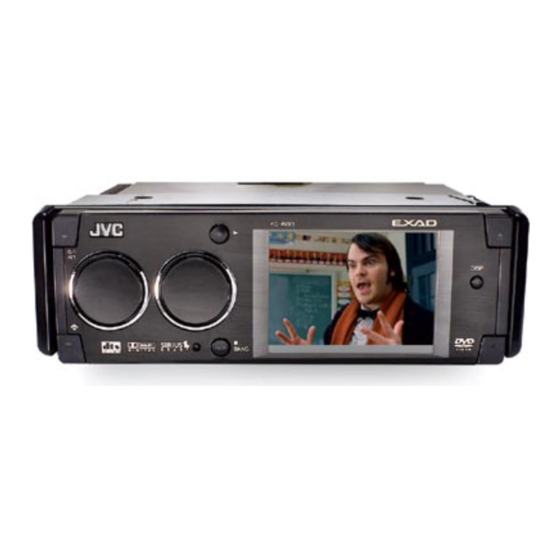
KD-AVX1
SOURCE
MENU
T/P
TABLE OF CONTENTS
COPYRIGHT © 2005 Victor Company of Japan, Limited
KD-AVX1
OK
BACK BAND
Area suffix
J ------------- Northern America
E ------------- Southern Europe
A ------------------------ Australia
UT ------------------------- Taiwan
UN --------------------- Indonesia
U -------------------- Other Areas
DISP
D
No.MA165
2005/5
Advertisement
Table of Contents

Related Manuals for JVC KD-AVX1


Summary of Contents for JVC KD-AVX1
-
Page 1: Table Of Contents
SERVICE MANUAL DVD/CD RECEIVER MA165 2005 KD-AVX1 Area suffix J ------------- Northern America E ------------- Southern Europe A ------------------------ Australia UT ------------------------- Taiwan UN --------------------- Indonesia U -------------------- Other Areas KD-AVX1 DISP SOURCE MENU BACK BAND Lead free solder used in the board (material : Sn-Ag-Cu, melting point : 219 Centigrade) TABLE OF CONTENTS PRECAUTIONS . - Page 2 SPECIFICATION for NORTHERN AMERICA version AUDIO AMPLIFIER SECTION × Ω Power Output 20 W RMS 4 Channels at 4 and [< or =] 1% THD+N Ω Signal to Noise Ratio 80 dBA (reference: 1 W into 4 Ω Ω Ω Load Impedance to 8 allowance)
- Page 3 for EUROPE version AUDIO AMPLIFIER SECTION Maximum Power Output Front 50 W per channel Rear 50 W per channel Ω Continuous Power Output (RMS) Front 20 W per channel into 4 , 40 Hz to 20 000 Hz at no more than 0.8% total harmonic distortion.
- Page 4 for ASIA & AUSTRALIA version AUDIO AMPLIFIER SECTION Maximum Power Output Front 50 W per channel Rear 50 W per channel Ω Continuous Power Output (RMS) Front 20 W per channel into 4 , 40 Hz to 20 000 Hz at no more than 0.8% total harmonic distortion.
-
Page 5: Precautions
SECTION 1 PRECAUTIONS Safety Precautions Burrs formed during molding may be left over on some parts of the chassis. Therefore, pay attention to such burrs in the case of preforming repair of this system. Please use enough caution not to see the beam directly or touch it in case of an adjustment or operation check. - Page 6 Preventing static electricity Electrostatic discharge (ESD), which occurs when static electricity stored in the body, fabric, etc. is discharged, can destroy the laser diode in the traverse unit (optical pickup). Take care to prevent this when performing repairs. 1.2.1 Grounding to prevent damage by static electricity Static electricity in the work area can destroy the optical pickup (laser diode) in devices such as CD players.
- Page 7 Important for laser products 5.CAUTION : If safety switches malfunction, the laser is able 1.CLASS 1 LASER PRODUCT to function. 2.DANGER : Invisible laser radiation when open and inter 6.CAUTION : Use of controls, adjustments or performance of lock failed or defeated. Avoid direct exposure to beam. procedures other than those specified here in may result in 3.CAUTION : There are no serviceable parts inside the hazardous radiation exposure.
-
Page 8: Specific Service Instructions
SECTION 2 SPECIFIC SERVICE INSTRUCTIONS This service manual does not describe SPECIFIC SERVICE INSTRUCTIONS. 1-8 (No.MA165) -
Page 9: Disassembly
SECTION 3 DISASSEMBLY Main body section 3.1.1 Removing the panel assembly (See Fig.1) (1) Push the button(detach) in the lower right part of the panel assembly. Panel assembly (2) Remove the panel assembly. Button(detach) Fig.1 3.1.2 Removing the side heat sink (See Fig.2) Reference: Remove the panel assembly as required. - Page 10 3.1.3 Removing the top chassis assembly (See Figs.3 to 6) • Remove the panel assembly and side heat sink. (1) From the top side of the main body, remove the two screws Top chassis assembly C attaching the top chassis assembly. (See Fig.3.) (2) From the back side of the main body, remove the two screws C attaching the top chassis assembly.
- Page 11 3.1.4 Removing the front chassis assembly (See Fig.7) • Remove the panel assembly, side heat sink and top chassis assembly. Top chassis assembly (1) From the both sides of the top chassis assembly, remove the two screws E attaching the front chassis assembly. (2) Remove the front chassis assembly from the top chassis assembly.
- Page 12 3.1.6 Removing the main sub board (See Fig.10) • Remove the panel assembly, side heat sink, top chassis as- sembly and DVD mechanism assembly. Main sub board (1) From the top side of the DVD mechanism assembly, re- lease the lock of the connector CN965 on the main sub board and disconnect the card wire.
- Page 13 3.1.10 Removing the connector board (See Figs.13 to 15) • Remove the panel assembly, side heat sink, top chassis as- sembly and front bracket assembly. Torsion spring Front bracket assembly (1) From the front side of the front bracket assembly, remove the two screws M.
- Page 14 3.1.11 Removing the main board (See Figs.16 and 17) • Remove the panel assembly, side heat sink, top chassis as- sembly, loading unit assembly and arm bracket assemblies Rear bracket (L)/(R). (1) From the back side of the main body, remove the screw P attaching the rear bracket.
- Page 15 3.1.12 Removing the rear bracket (See Fig.18) • Remove the panel assembly, side heat sink, top chassis as- sembly, loading unit assembly, arm bracket assemblies (L)/(R) Wire holder Car cable and main board. (1) From the back side of the main board, remove the two Rear heat sink screws Q attaching the rear heat sink.
- Page 16 3.1.14 Removing the panel board (See Figs.20 and 21) • Remove the panel assembly. (1) From the back side of the panel assembly, remove the sev- Rear cover en screws U attaching the rear cover to the panel assem- bly. (See Fig.20.) (2) From the inside of the rear cover, release the lock of the connector CN582...
- Page 17 DVD mechanism assembly 3.2.1 Removing the mechanism control board (See Fig.1) Caution: Before disconnecting the flexible wire extending from the DVD Lug wire Flexible wire pickup, solder the short-circuit point on the flexible wire using Feed motor a grounding soldering iron. If you do not follow this instruction, Double tape the DVD pickup may be damaged.
- Page 18 3.2.2 Removing the top cover (See Fig.2) (1) Remove the two screws D attaching the top cover on the back of the body. (2) Remove the top cover upward. Reference: When reassembling, set part b of the top cover under the bending part c of the chassis frame.
- Page 19 3.2.4 Removing the clamper unit (See Fig.5 to 7) • Remove the top cover and the mechanism section. (1) Remove the clamper2 spring on the bottom of the mecha- Clamper2 spring nism section. (See Figs.5.and 6.) (2) Release the part d of the clamper spring from the bending part of the chassis base assembly.
- Page 20 Clamper unit Clamper spring Fig.8 Clamper unit Notch Fig.9 1-20 (No.MA165)
- Page 21 3.2.6 Removing the front unit (See Fig.10 to 12) • Remove the top cover and the mechanism section. (1) Disconnect the flexible wire from connector CN202 on the mechanism control board at the bottom of the body. (See Front unit Fig.10.) (2) Remove the screw G attaching the front unit on the top of the body.
- Page 22 3.2.7 Removing the loading arm assembly (See Fig.13 , 14) • Remove the top cover, the mechanism section and the front unit. (1) From the top of the body, move the loading arm assembly from the front side upward, and release the bosses from the right and left joints k and m of the chassis base assem- bly.
- Page 23 3.2.8 Removing the rod (L)(R)/roller assembly (See Fig.15 and 16) • Remove the top cover, the mechanism section, the front unit and the loading arm assembly. Collar Collar (1) Release the rod (L) and (R) from the joints q at the bottom of the loading arm assembly (See Fig.15.) (2) Remove the roller assembly from the loading arm assem- bly.
- Page 24 3.2.9 Removing the DVD pickup assembly (See Fig.17 to 19) • Remove the mechanism control board. (1) From the bottom of the body, turn the feed gear in the di- Feed gear rection of the arrow to move the DVD pickup outwards. (See Fig.17.) (2) Remove the screw J attaching the thrust spring.
- Page 25 3.2.10 Removing the spindle motor (See Fig.20) • Remove the mechanism control board. Remove the two screws L attaching the spindle motor on the Spindle motor bottom of the body. Caution: Perform adjustment when reattaching the spindle motor. Fig.20 3.2.11 Removing the feed motor assembly (See Fig.21 and 22) •...
-
Page 26: Adjustment
SECTION 4 ADJUSTMENT Test instruments required for adjustment Standard measuring conditions (1) Digital oscilloscope (100MHz) Power supply voltage DC14.4V(11 to 16V) (2) Jitter meter Load impedance 4Ω(2 Speakers connection) (3) Digital tester Line Output 20KΩ (4) Electric voltmeter (5) Tracking offset meter Caution: (6) Test Disc : VT501 or VT502 Be sure to attach the heat sink and rear bracket onto the power... - Page 27 Adjustment method for jitter After replacing the pickup, set the unit in the service mode to display a jitter value on the LCD. Confirm that the jitter value measured with a jitter meter is within 12% of the jitter value displayed on the LCD. If it is within 12%, then adjustment is not necessary.
- Page 28 Jitter value conversion table Load the test DVD and set the unit to the service mode. A jitter value converted to the hex value is displayed on the LCD. Refer to the corresponding decimal notation value shown in the following Jitter Conversion Table. The adjustment is OK if the jitter value measured with a jitter meter is within 12% of the jitter value displayed on the LCD.
- Page 29 Service mode 4.6.1 Standard input/output conditions Power supply voltage DC14.4V(11 to 16V) Load impedance 4Ω(2 Speakers connection) Line Output 20KΩ 4.6.2 Service mode setting procedure (The DVD does not need to be loaded before starting the following procedure.) [STANDBY/ON ATTENUATOR] button [MENU] button [OK] button [EJECT] button...
- Page 30 2. Service mode 2 Keep this state more than 2 seconds while continuing pressing the [DISP] button, [VOLUME-] button and [EJECT] button sequentially. Screen indication SERVICE MODE2 SERVICE MODE 2 INITIALIZE DVD Press the [OK] button. Full initialization of EEPROM of a DVD unit (It is included a permanent domain) After clear completion, this indication is continued till an effective key is input.
- Page 31 Screen indication SERVICE MODE SERVICE MODE VERSION ERROR READ AREA/REGION ERROR CLEAR TEMPERATURE MEMORY CHECK DVD NTSC/PAL DVD CHECK MODE Exchanging it operate a menu of a service mode with the [UP] button and [DOWN] button. Micon version indication VERSION Operate choice of a menu with MAIN a [OK] button.
- Page 32 ERROR READ DVD ERROR READ CD ERROR READ MECHA ERROR READ DVD ERROR READ TOTAL Reading of a DVD unit error history Reading of a history of an error stored in a DVD unit Indication of latest three error codes and first five error code Indication of total error count Error code...
- Page 33 4. Service mode 4 Keep this state more than 2 seconds while continuing pressing the [DISP] button, [BACK] button and [EJECT] button sequentially. Screen indication SERVICE MODE4 RDS S MODE MONITOR S MODE Exchanging it operate a menu of a service mode with the [UP] button and [DOWN] button.
- Page 34 4.6.5 Error code tables Mechanism error code Error code Detailed error code Error contents Details Disc loading error B1 time out 0x99 0x0011 C1 time out 0x99 0x0012 D1 time out 0x99 0x0013 C2 time out 0x99 0x0014 B2 time out 0x99 0x0015 A2 time out...
- Page 35 4.6.6 Running mode Indication Explanation Operation contents of 1 cycle In mecha error In disc error SDRAM inspection RUNNING1 MECHA Door mecha running1 Panel close Panel open RUNNING2 MECHA Door mecha running1 Panel close Panel open Panel detach position Panel angle 3 position Panel angle 1 position Panel angle 2 position RUNNING3 DVD DVD+Door mecha running1...
- Page 36 4.6.8 Update method of firm ware Power on. Insert the disc which a farm was written in at. Screen indication VERSION UP DISC PROGRAM WRITING MODE Current version CURRENT VERSION 0735 NEW VERSION 0795 Version to write in READING... If "PLEASE EJECT" was displayed after the writing end, take out a disc.
- Page 37 4.6.9 Monitor adjustment When adjusting, switch on the main unit and insert a test disc (VT-501). And play the test disc and pause it. (Exit for VCO FREE-RUN adjustment) R/W CHROMA 1 1. Set the service mode 4. 2. Exchanging it operate a menu of a service mode with the [UP] button and [DOWN] button. 3.
-
Page 38: Troubleshooting
SECTION 5 TROUBLESHOOTING 16 PIN CORD DIAGRAM [for E version] Black Green GN/BK WH/BK Violet VI/BK GY/BK Gray Blue White Yellow Orange Brown BL/WH L. GN L.GN Light Green OR/WH BL/WH OR/WH Choking Coil MEMORY REMOTE BL/WH OR/WH VI/BK GY/BK WH/BK GN/BK L.GN... - Page 39 16 PIN CORD DIAGRAM [for A, J, U, UN, UT version] GN/BK WH/BK Black Green VI/BK GY/BK Violet Gray Blue White Yellow BL/WH L. GN Orange Brown OR/WH L.GN Light Green GN/BK WH/BK VI/BK GY/BK BL/WH REMOTE TEL MUTING OR/WH ILLUMINATION CONTROL Choking Coil...
- Page 40 Victor Company of Japan, Limited AV & MULTIMEDIA COMPANY CAR ELECTRONICS CATEGORY 10-1,1chome,Ohwatari-machi,Maebashi-city,371-8543,Japan (No.MA165) Printed in Japan...
-
Page 41: Parts List
PARTS LIST [ KD-AVX1 ] * All printed circuit boards and its assemblies are not available as service parts. Area suffix J ------------- Northern America E ------------- Southern Europe A ------------------------ Australia UT -----------------------------Taiwan UN ---------------------- Indonesia U -------------------- Other Areas... - Page 42 Exploded view of general assembly and parts list Block No. Connector board Main sub board 98 67 Main b Switch board Panel board...
- Page 43 Main board Switch board Panel switch board 76 76 U,UN,UT,A,E...
- Page 44 General Assembly Block No. [M][1][M][M] Symbol No. Part No. Part Name Description Local QYSDST2004ZA TAP SCREW M2 x 4mm(x2) LV44173-001A PWB BRACKET QYSDST2004ZA TAP SCREW M2 x 4mm GE40278-001A SHEET LV44263-001A SPACER LV11077-001A TOP CHASSIS LV35764-001A FRONT CHASS ASS GE40156-001A BLIND LV40846-017A...
- Page 45 BUTTON (BACK) LV35776-001A CAP (POWER) LV35777-001A CAP (EJECT) LV35778-001A CAP (T/P) LV35779-001A BUTTON (POWER) LV35780-001A BUTTON (EJECT) LV35781-001A BUTTON (T/P) LV43184-002A JVC BADGE VKZ4777-006 MINI SCREW (x7) VKZ4777-009 MINI SCREW (x5) LV44299-001A SW PWB SHEET LV40849-014A SPACER(R) QLD0366-001 LCD MODULE LCD1...
- Page 46 DVD mechanism assembly and parts list Block No. Grease FMU-JD4-2D = JVS-1003 = MOBIL-1 = JVG-31N = JC-803B = 1401C BACK SIDE AFTER SET PICK UP SA. APPLY GREASE INSIDE The parts without symbol number are not service.
- Page 47 DVD mechanism Block No. [M][J][M][M] Symbol No. Part No. Part Name Description Local VKZ4539-056 MINI SCREW (x2) QYSPSFT2040ZA TAP SCREW M2 x 4mm LV43481-001A COOLING RUBBER (x2) LV10674-001A CHASSIS FRAME LV30225-0J6A SPACER (x2) VKZ4539-056 MINI SCREW VYSA1R4-056 SPACER LV33684-001A DAMPER(F) (x2) LV33685-001A...
- Page 48 Symbol No. Part No. Part Name Description Local LV43010-001A L.S.GEAR LV43063-001A L.S.COLLAR LV43011-001A THRUST SPRING QYSPSFT2040ZA TAP SCREW M2 x 4mm LV33624-001A HOLDER(M) VKZ4539-056 MINI SCREW (x2) LV21288-001A HOLDER(S) VKZ4539-056 MINI SCREW (x2) LV43064-001A ROD(M) LV43065-001A ROD(S) LV43066-001A SUB SHAFT VKZ4730-002 SPECIAL SCREW (x3)
-
Page 49: Electrical Parts List
Electrical parts list Main board Symbol No. Part No. Part Name Description Local Block No. [0][1] Q951 RT1N141C-X TRANSISTOR Symbol No. Part No. Part Name Description Local Q952 2SA1530A/QR/-X TRANSISTOR Q953 RT1N441C-X TRANSISTOR Q991 2SC3928A/QR/-X TRANSISTOR IC31 SAA6579T-X IC131 NJM2160BV-X MC2838-X... - Page 50 Symbol No. Part No. Part Name Description Local Symbol No. Part No. Part Name Description Local NCB31CK-223X C CAPACITOR 0.022uF 16V K C252 NDC31HJ-101X C CAPACITOR 100pF 50V J QERF1HM-225Z E CAPACITOR 2.2uF 50V M C261 QERF1EM-475Z E CAPACITOR 4.7uF 25V M C101 NBE41AM-476X...
- Page 51 Symbol No. Part No. Part Name Description Local Symbol No. Part No. Part Name Description Local C826 QERF1CM-476Z E CAPACITOR 47uF 16V M NRSA63J-103X MG RESISTOR 10kΩ 1/16W J C827 QEZ0595-477Z E CAPACITOR 470uF NRSA63J-0R0X MG RESISTOR 0Ω 1/16W J C828 QEZ0595-477Z E CAPACITOR...
- Page 52 Symbol No. Part No. Part Name Description Local Symbol No. Part No. Part Name Description Local R231 NRSA63J-104X MG RESISTOR 100kΩ 1/16W J A,J,U, R721 NRSA63J-473X MG RESISTOR 47kΩ 1/16W J UN,U R232 NRSA63J-363X MG RESISTOR 36kΩ 1/16W J R233 NRSA63J-243X MG RESISTOR...
- Page 53 Symbol No. Part No. Part Name Description Local Symbol No. Part No. Part Name Description Local R804 NRSA63J-223X MG RESISTOR 22kΩ 1/16W J R937 NRSA63J-0R0X MG RESISTOR 0Ω 1/16W J R805 NRSA63J-391X MG RESISTOR 390Ω 1/16W J R938 NRSA63J-105X MG RESISTOR 1MΩ...
- Page 54 Symbol No. Part No. Part Name Description Local Symbol No. Part No. Part Name Description Local CN860 QNZ0095-001 CONNECTOR CN861 QGA2001C1-02 CONNECTOR W-B (1-2) D401 NECBB205/WQR/-X E CAPACITOR #NCVpF 0 CN871 QGA2501C1-02 CONNECTOR W-B (1-2) D402 NECBB205/WQR/-X E CAPACITOR #NCVpF 0 CN881 QGA2501C1-02...
- Page 55 Symbol No. Part No. Part Name Description Local Symbol No. Part No. Part Name Description Local C609 NCB31CK-103X C CAPACITOR 0.01uF 16V K C4001 NCB31CK-473X C CAPACITOR 0.047uF 16V K C611 NDC31HJ-120X C CAPACITOR 12pF 50V J C4002 NCB31CK-103X C CAPACITOR 0.01uF 16V K...
- Page 56 Symbol No. Part No. Part Name Description Local Symbol No. Part No. Part Name Description Local R472 NRSA63J-0R0X MG RESISTOR 0Ω 1/16W J R601 NRSA63J-121X MG RESISTOR 120Ω 1/16W J R473 NRSA63J-0R0X MG RESISTOR 0Ω 1/16W J R602 NRSA63J-121X MG RESISTOR 120Ω...
- Page 57 Connector board Symbol No. Part No. Part Name Description Local Block No. [0][3] R6652 NRSA63J-471X MG RESISTOR 470Ω 1/16W J R6653 NRSA63J-0R0X MG RESISTOR 0Ω 1/16W J Symbol No. Part No. Part Name Description Local R6901 NRSA63J-473X MG RESISTOR 47kΩ...
- Page 58 Symbol No. Part No. Part Name Description Local Symbol No. Part No. Part Name Description Local C202 NCB31CK-104X C CAPACITOR 0.1uF 16V K C398 NCB31CK-104X C CAPACITOR 0.1uF 16V K C203 NCS31HJ-271X C CAPACITOR 270pF 50V J C399 NCB31CK-104X C CAPACITOR 0.1uF 16V K...
- Page 59 Symbol No. Part No. Part Name Description Local Symbol No. Part No. Part Name Description Local R259 NRSA63J-103X MG RESISTOR 10kΩ 1/16W J R431 NRSA63J-472X MG RESISTOR 4.7kΩ 1/16W J R260 NRSA63J-470X MG RESISTOR 47Ω 1/16W J R432 NRSA63J-472X MG RESISTOR 4.7kΩ...
- Page 60 Packing materials and accessories parts list Block No. No additional / supplemental order of WARRANTY CARDs are available. A1 A3 A1 A3 J version UT,UN version U,A version A1 A3 A4 E version A20 A21 A22 A23 J version KIT: A5 A6 A7 A8 A9 A10 U,E,A version 3-20...
- Page 61 Packing and Accessories Block No. [M][3][M][M] Symbol No. Part No. Part Name Description Local LVT1323-001B INST BOOK ENG GER FRE DUT LVT1322-001B INST BOOK ENG SPA FRE LVT1324-001B INST BOOK ENG CHI(TAIWAN) THA LVT1324-003B INST BOOK ENG INA LVT1324-004B INST BOOK ENG CHI(TAIWAN) LVT1323-002B...
- Page 62 SCHEMATIC DIAGRAMS DVD/CD RECEIVER KD-AVX1 CD-ROM No.SML200505 Area suffix J ------------- Northern America E ------------- Southern Europe A ------------------------ Australia UT ------------------------- Taiwan UN --------------------- Indonesia U -------------------- Other Areas KD-AVX1 DISP SOURCE MENU BACK BAND Lead free solder used in the board (material : Sn-Ag-Cu, melting point : 219 Centigrade)
-
Page 63: Safety Precaution
Safety precaution Burrs formed during molding may be left over on some parts of the chassis. Therefore, pay attention to such burrs in the case of preforming repair of this system. Please use enough caution not to see the beam directly or touch it in case of an adjustment or operation check. - Page 64 < M E M O >...
-
Page 65: Block Diagram
Block diagram DVD servo control section EPDI EPDO EPSK A,B,C,D,E,F,F1CD,F2CD FOCUS EPCS IC481 F1DVD,F2DVD,VREFH LPC1,LPC2 & EPROM TRACKING COIL LPCO1 MA0 to MA11,MDQ0 to MDQ15 Q101 DVDLDCUR DQM0,DQM1,BA0,BA1,MCK IC399 NWE,NCSM,NCAS,NRAS Q102 SDRAM LPCO2 Q103 AOUT3,BCK CDLDCUR LRCK,PCMCLK Q104 DACPDN /DRVMUTE PICK UP DACOCS TRDRV... -
Page 66: Line Out
IC302 S2UDT 2nd AUDIO 2nd AUDIO & REVERSE CPURST E.VOLUME GEAR SIGNAL HPDATA SI/SO HPCK JD4LRMUTE HPSTB IC941 Q849 UCS,JD4SCS JD4SCLK JVC BUS JD4U2SDT IC971 BKLAMP ST_REM JD4S2UDT BUSSO IC972 CPURST BUSSCK REMOTE LEVEL BUSINT I/O,SI/SO CONV. J/E version EEP_DAI... - Page 67 Standard schematic diagrams Main amplifier section R115 R215 C115 C215 LINE-L LINE-G 100p 100p LINE-R C338 4.7/25 IC332 R337 R338 CD4053BPW-X IC331 C337 NJM4565V-X 220p C335 R334 R335 C336 4.7/25 68k 0.033 R336 SW_THROUGH SW_INV R331 QAM0556-001 R123 C128 C125 C126 0.082 R126...
- Page 68 CN311 QGA2501C1-06 R115 R215 R105 R106 C109 4.7/25 C115 C215 HPDATA C106 C104 C105 R108 R109 HPCK 100p 100p C102 HPSTB R104 100p 150p 4.7/25 Q101 4.7k 4.7/25 2SD1781K/QR/-X R110 R101 C332 2.2k NQR0022-005X NQR0022-005X NQR0022-005X 3BPW-X L101 Q341 L301 2SD1781K/QR/-X L201 Q201...
- Page 69 Panel-A section R649 IC601 MB87P2040PMT R601 C634 R602 R603 R604 K603 GDC-G C601 NQR0022-005X C602 C604 R605 K604 GDC-B C603 NQR0022-005X C633 0.01 IC511 R606 2.7k C605 22/10 C606 R607 K605 GDC-R NQR0022-005X RA518 NRZ0065-102X C607 C608 NQR0022-005X C632 C610 L604 R608 C611...
- Page 70 R584 K581 IC585 GP1UX511RK R587 TP515 TP525 IC511 L501 NQL79GM-100X R531 RA518 NRZ0065-102X C505 0.01 R546 RA519 NRZ0065-102X R545 R544 R502 R573 RA514 DC_INT R574 470k SPCE R518 R522 R504 RA513 MN103S77NDX C506 RA512 0.01 Q451 2SA1530A/QR/-X V_SEN R575 R451 R452 R453 R454...
- Page 71 Panel-B section R6903 R6906 Q651 R660 2SC3928A/QR/-X R661 Q656 2SC3928A/QR/-X R685 R671 330k R678 C681 4.7/6.3 R669 100k C672 0.001 R679 C671 100p C6901 C670 0.01 C669 47/6.3 D6901 L653 NQL79GM-100X MA2SV03-X IC651 AN2546FH-AV TP651 TP661 TP671 TP681 C682 C683 L655 R680 4.7/6.3...
- Page 72 UDZS5.6B-X UDZS5.6B-X UDZS5.6B-X UDZS5.6B-X UDZS5.6B-X UDZS5.6B-X RESET REMOCON KEYDATA DISPDATA DISPCE DISPCLK ACC5V VIDEO MIC0N3.3V R597 RESET REMOCON KEYDATA DISPDATA DISPCE DISPCLK TP652 TP662 TP672 TP682 RGB-HD RGB-VD TP653 TP663 Q6651 TP673 470X 2SC3928A/QR/-X TP683 R6651 C695 RGB-R RGB-HD K582 RGB-VD K583 Q693...
- Page 73 Connecting section CN965 QGF0523F1-45W R9001 R9012 R9013 R9011 C9007...
- Page 74 CN964 CN963 QGZ2203L1-20X QGF1038F1-20X CN892 S896 QGF0523F1-07W NSW0183-001X S895 NSW0183-001X S894 NSW0183-001X S893 NSW0183-001X S892 NSW0183-001X S891 NSW0183-001X SHEET 4 2-10...
- Page 75 DVD servo control section P3.3V K399 NQR0502-001X IC399 K4S281632F-UC75 C399 IC398 0.1/16 SG32M90TFIR3 MDQ0 MDQ15 0.1/16 EXADT15 EXADR16 MDQ1 MDQ14 C392 R399 EXADT14 MDQ2 MDQ13 EXADT13 P3.3V C393 EXADT12 EXDAT15 MDQ3 MDQ12 0.1/16 EXADT11 EXDAT7 MDQ4 MDQ11 EXADT10 EXDAT14 EXADT9 EXDAT6 0.1/16 MDQ5...
- Page 76 D3.3V R300 IC303 P3.3V R301 K301 NQR0502-001X D1.2V D3.3V IC302 BA00HC5WF-X R332 EXDAT8 DGND 0.1/16 TP325 CN402 TP318 TP316 QGF0522F1-06W C315 0.1/16 R369 R367 K425 NQL093K-1R8X K427 K428 C311 0.1/16 K429 NQL093K-1R8X R361 AOUT3 NI NI NI NI NQL093K-1R8X K420 R358 L306 K421...
-
Page 77: Printed Circuit Boards
Printed circuit boards Main board Lead free solder used in the board (material : Sn-Ag-Cu, melting point : 219 Centigrade) Forward side (Main board) C841 CN361 R803 Q841 PP11 R802 R801 C802 D842 C844 CN311 C804 C911 D861 R164 C913 C222 C912 C801... - Page 78 Reverse side (Main board) IC912 IC801 C262 C162 C252 C152 CN901 CN361 PP11 C841 C343 D841 Q844 CN311 C844 C805 C861 CN860 Q842 C222 R902 C122 C341 C914 R903 C842 R215 R115 C315 R901 D983 C215 C115 R315 D901 D871 R872 R871 C843...
- Page 79 Panel board Lead free solder used in the board (material : Sn-Ag-Cu, melting point : 219 Centigrade) Forward side (Switch board) IC585 R587 C586 B471 (Panel board) D582 D581 D583 B657 D585 D587 D589 D591 B656 D592 D593 D594 B655 C510 C509 R580...
- Page 80 Reverse side (Switch board) R478 R477 R476 R475 C478 R474 R473 R472 R471 R489 R490 C473 (Panel board) R488 L471 R487 R486 R469 TP476 C479 C481 C484 C486 D6701 C487 D6702 C488 C6702 C483 C6703 C6701 D6651 R647 R6653 R633 C6704 R632 C6705...
- Page 81 Connector board Lead free solder used in the board (material : Sn-Ag-Cu, melting point : 219 Centigrade) Forward side (Panel switch board) (Connector board) Reverse side (Connector board) CN963 CN964 (Panel switch board) 2-17...
- Page 82 < M E M O >...
- Page 83 Front end board Lead free solder used in the board (material : Sn-Ag-Cu, melting point : 219 Centigrade) Forward side R435 C431 R438 C433 B204 C432 K445 IC411 C533 IC401 C532 R531 C452 C453 C454 R535 K451 K301 C451 R355 C361 R356 C302...
- Page 84 Front end board Lead free solder used in the board (material : Sn-Ag-Cu, melting point : 219 Centigrade) Reverse side C404 R403 C403 C405 B201 R404 R402 B202 K443 R421 B203 R521 C402 C522 TP455 R401 K442 TP433 R365 R366 C368 TP416 TP446...
- Page 85 Victor Company of Japan, Limited AV & MULTIMEDIA COMPANY CAR ELECTRONICS CATEGORY 10-1,1chome,Ohwatari-machi,Maebashi-city,371-8543,Japan Printed in Japan (No.MA165SCH)