Table of Contents
Advertisement
QQ
3 7 63 1515 0
TE
L 13942296513
www
.
011768
PA
200501-38850
http://www.xiaoyu163.com
CONTENTS
SPECIFICATIONS
CIRCUIT BOARDS
PARTS LIST
Block Diagram & LEVEL DIAGRAM
(ブロックダイアグラム&レベルダイアグラム)
x
ao
u163
y
i
http://www.xiaoyu163.com
MIXING CONSOLE
2 9
8
SERVICE MANUAL
Q Q
3
6 7
1 3
1 5
(目次)
(総合仕様)
................................................ 3/5
(寸法図)
............................................................ 7
(パネルレイアウト)
(ユニットレイアウト)
(結線図)
.................................................................. 13
(分解手順)
(LSI端子機能表)
(ICブロック図)
(シート基板図)
(検査)
....................................................... 30/35
(総回路図)
co
.
Copyright (c) Yamaha Corporation. All rights reserved. PDF-K
9 4
2 8
0 5
8
2 9
9 4
2 8
..................................... 8
................ 12
.......................... 14
............................... 19
.................................. 20
....................................... 22
m
HAMAMATSU, JAPAN
MG12/4FX
9 9
9 9
1
'05.02
Advertisement
Table of Contents

Related Manuals for Yamaha MG12/4FX


Summary of Contents for Yamaha MG12/4FX
- Page 1 IC BLOCK DIAGRAM ........20 (シート基板図) CIRCUIT BOARDS ........22 INSPECTIONS (検査) ............30/35 PARTS LIST BLOCK DIAGRAM & LEVEL DIAGRAM (ブロックダイアグラム&レベルダイアグラム) OVERALL CIRCUIT DIAGRAM (総回路図) u163 011768 HAMAMATSU, JAPAN 200501-38850 Copyright (c) Yamaha Corporation. All rights reserved. PDF-K ’05.02 http://www.xiaoyu163.com...
- Page 2 IMPOR TANT NOTICE This manual has been provided for the use of authorized Yamaha Retailers and their service personnel. It has been assumed that basic service procedures inherent to the industry, and more specifically Yamaha Products, are already known and under- stood by the users, and have therefore not been restated.
-
Page 3: Specifications
MG12/4FX 3 7 63 1515 0 SPECIFICATIONS ■ Electrical Characteristics Conditions UNIT (THD+N) 20 Hz-20 kHz @+14 dBu 600 ohms (CH1 to 4) with Total Harmonic Distortion Signal input CH ST Switches are On, Signal input CH Fader, (MIC to ST OUT) -
Page 4: Input Specifications
MG12/4FX 3 7 63 1515 0 ■Input Specifications Input Appropriate Max. Before Nominal Connector Input Connector Gain Sensitivity* Impedance Impedance Clipping Level Specifications -80 dBu -60 dBu -40 dBu (0.078 mV) (0.775 mV) (7.75 mV) MIC INPUT XLR-3-31 type 50-600 Ω... - Page 5 MG12/4FX 3 7 63 1515 0 総合仕様 ■ 電気的特性 条件 最小 標準 最大 単位 (THD+N)20 Hz ∼20 kHz @+14 dBu 600 ohms (CH1 to 4)(信号入力チャンネルST スイッチ=ON 、信号入力チャンネル 全高調波歪率(MIC →ST OUT) % フェーダー、ST Master フェーダー=ノミナルレベル) 20 Hz ∼20 kHz @+4 dBu 600 ohms 周波数特性(MIC →ST OUT)
- Page 6 MG12/4FX 3 7 63 1515 0 ■ 入力仕様 最大ノンク 入力イン 入力端子名称 ゲイン 適合インピーダンス ノミナルレベル 端子仕様 感度 ピーダンス リップレベル -80 dBu -60 dBu -40 dBu (0.078 mV ) (0.775 mV ) (7.75 mV ) MIC INPUT XLR‐ 3‐ 31 タイプ...
- Page 7 MG12/4FX 3 7 63 1515 0 (寸法図) DIMENSIONS L 13942296513 317.4 【ラック取り付け時】 u163 Units: mm (単位) http://www.xiaoyu163.com...
-
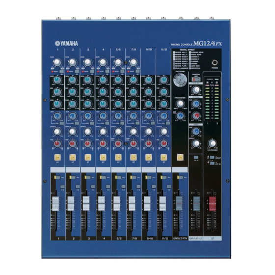
Page 8: Panel Layout
MG12/4FX 3 7 63 1515 0 (パネルレイアウト) PANEL LAYOUT Channels Channels Channels 1 to 4 5/6 and 7/8 9/10 and 11/12 GAIN Control (Monaural) (Stereo) (Stereo) PEAK Indicator チャンネル チャンネル チャンネル 80 Switch (High Pass Filter) 1∼4 5/6、7/8 9/10、11/12 Equalizer (HIGH, MID, and LOW) (モノラル)... - Page 9 MG12/4FX 3 7 63 1515 0 (マスターコントロール部) Master Control Section ST Master Fader GROUP 1-2 Fader TO ST Switch Master SEND RETURN 2TR IN Control PHANTOM +48V Switch Level-Meter Signal switches (ST-GROUP Toggle Switch and 2TR IN Switch) C-R/PHONES Control...
- Page 10 MG12/4FX 3 7 63 1515 0 Rear Input/Output Section (リア入出力部) チャンネル INPUT 端子 Channel Input Jacks L 13942296513 INSERT I/O 端子 INSERT I/O Jacks チャンネル INPUT 端子 Channel Input Jacks GROUP OUT (1、2) 端子 GROUP OUT (1, 2) Jacks ST OUT (L、R) 端子...
- Page 11 MG12/4FX 3 7 63 1515 0 Connector Polarities INPUT OUTPUT Pin 1: Ground MIC INPUT, ST OUT Pin 2: Hot (+) Pin 3: Cold (-) LINE INPUT (monaural channels), Tip: Hot (+) GROUP OUT, ST OUT, C-R OUT Ring: Cold (-)
- Page 12 MG12/4FX 3 7 63 1515 0 (ユニットレイアウト) CIRCUIT BOARD LAYOUT JACK JACK MAIN(2/2) MAIN(2/2) L 13942296513 MAIN(1/2) u163 http://www.xiaoyu163.com...
- Page 13 MG12/4FX 3 7 63 1515 0 (結線図) WIRING 1. Jumper wire bending in the dimension of figure. WC703300 ジャンパーワイヤーを図の寸法に曲げます。 15±1mm 10±1mm To circuit board Jack To circuit board Main ジャック基板へ メイン基板へ 2.Before attaching circuit board MAIN & JACK to panel, insert wiring ass'y to each connector.
-
Page 14: Disassembly Procedure
MG12/4FX 3 7 63 1515 0 DISASSEMBLY PROCEDURE (分解手順) ボトムに負荷がかからないように台に置くなどして、 注 Take care to avoid excess load to the bottom by putting the unit on a table or the like. 意して作業してください。 Rack Mount Angle ラックアングル (所要時間:各約 1 分) (Time required: About 1 minute each) [420]のネジ2本を外し、... - Page 15 MG12/4FX 3 7 63 1515 0 Side Cover サイドカバー、シート PS (Time required: About 6 minutes each) (所要時間:各約 6 分) Remove the bottom cover. (See procedure 2.) ボトムカバーを外します。 (2 項参照) Side Cover L: サイドカバー L: 3-2-1 Remove the Rack Mount Angle L. (See procedure 1.) 3-2-1 ラックアングル...
- Page 16 MG12/4FX 3 7 63 1515 0 Power Supply Unit(シートPS) Heat Sink (ヒートシンク) IC01 IC01 IC02 IC02 IC03 IC03 IC04 IC04 IC05 IC05 [360] Side Cover R(サイドカバ−R) (+バインドBタイト) [360]: Bind Head Tapping Screw-B 3.0X8 MFZN2BL (EP600190) (図2) Fig.2 Fig.1 (図1) シート...
- Page 17 MG12/4FX 3 7 63 1515 0 Power Switch and AC Connector 電源 SW と AC コネクタ (所要時間:約 6 分) (Time required: About 6 minutes) ボトムカバーを外します。 (2 項参照) Remove the bottom cover. (See procedure 2) サイドカバーR、 シートPSを外します。 (3-3項参照) Remove the side cover R and PS circuit board.
- Page 18 MG12/4FX 3 7 63 1515 0 [200] Knob(PROGRAM) [270] (ノブ(PROGRAM) ) [270] [270] [270] [270]: Bonding Tapping Screw-B (ボンディングBタイト) 3.0X10 MFZN2BL (VQ049800) Photo.11 (写真11) Knob(FADER) (ノブ(フェーダー) ) (六角穴付きSタイト) [200]: Hex.Socket Set Screw 3.0X6 MFZN2BL (WD252600) Connector(コネクタ) JACK Photo.12 (写真12)
-
Page 19: Lsi Pin Description
MG12/4FX 3 7 63 1515 0 (LSI 端子機能表) LSI PIN DESCRIPTION YMW767-V (X3271A00) CPU DSP: ICM07 NAME FUNCTION NAME FUNCTION TESTN Input for TEST IOVDD IOVDD +3.3V PLLBPN PLL bypass select LBN/LWRN/PF6 External memory lower-byte enable PLLVDD PLLVDD +2.5V... -
Page 20: Ic Block Diagram
MG12/4FX 3 7 63 1515 0 (IC ブロック図) IC BLOCK DIAGRAM AK5381VT-E2 (X5219A00) DSP: ICM04 A/D Converter VA AGND VD DGND MCLK Pin No. Pin Name Function AINR Rch Analog Input Pin AINR CKS0 AINL Lch Analog input Pin... - Page 21 MG12/4FX 3 7 63 1515 0 NJM2068MD-TE2 (X3505A00) LB1412M-TE-R (X5838A00) DSP: ICM09, ICM11 MAIN(1/2) : ICH01,H02 MAIN(1/2) : IC103, 502,503,702,703,902-904,A02-A04, LED Driver B01-B03,C01-C03,D01-D03,E01,E03,F01, G01-G05 RESET OSC ILED NJM4556AL (XP844A00) MAIN(1/2) : ICH03 CURENT OUT2 DRIVER NJM4580M-D (TE2) (X5025A00) JACK: ICG06, 07...
- Page 22 MG12/4FX 3 7 63 1515 0 CIRCUIT BOARDS (シート基板図) DSP Circuit Board (X5022C0) ............22 PS Circuit Board (X5235B0) ............23 JACK Circuit Board (X5403C0) ............. 24 MAIN(1/2, 2/2) Circuit Board (X5024C0) ........28 Note: See parts list for details of circuit board component parts.
- Page 23 MG12/4FX 3 7 63 1515 0 PS Circuit Board Scale : 90/100 to MAIN(1/2)-CN102 to MAIN(1/2)-CNF01 to SW01 Component side (部品側) L 13942296513 Pattern side (パターン側) u163 http://www.xiaoyu163.com...
- Page 24 MG12/4FX 3 7 63 1515 0 JACK Circuit Board L 13942296513 to MAIN(1/2)-CN501 to MAIN(1/2)-CN501 to MAIN(1/2)-CN501 to MAIN(1/2)-CN501 to MAIN(1/2)-CN501 to MAIN(1/2)-CN501 to MAIN(1/2)-CN701 to MAIN(1/2)-CN701 to MAIN(1/2)-CN701 to MAIN(1/2)-CN701 to MAIN(1/2)-CN701 to MAIN(1/2)-CN701 to MAIN(1/2)-CN901 to MAIN(1/2)-CN901...
- Page 25 MG12/4FX 3 7 63 1515 0 Scale : 100/100 L 13942296513 /2)-CN901 /2)-CN901 /2)-CN901 /2)-CN901 /2)-CN901 /2)-CN901 to MAIN(1/2)-CNA01 to MAIN(1/2)-CNA01 to MAIN(1/2)-CNA01 to MAIN(1/2)-CNA01 to MAIN(1/2)-CNA01 to MAIN(1/2)-CNA01 to MAIN(1/2)-CND01 to MAIN(1/2)-CND01 to MAIN(1/2)-CND01 to MAIN(1/2)-CND01 to MAIN(1/2)-CND01...
- Page 26 MG12/4FX 3 7 63 1515 0 L 13942296513 u163 http://www.xiaoyu163.com...
- Page 27 MG12/4FX 3 7 63 1515 0 Scale : 100/100 L 13942296513 Pattern side (パターン側) u163 http://www.xiaoyu163.com...
- Page 28 MG12/4FX 3 7 63 1515 0 MAIN Circuit Board Scale : 50/100 to JACK-CN571 to JACK-CN771 to JACK-CN971 to JACK-CNA71 to JACK-CND71 to JACK-CNE71 to JACK-CNG71 to PS-CN02 to PS-CN03 L 13942296513 B version: compared to C version, only some patterns are different.
- Page 29 MG12/4FX 3 7 63 1515 0 to DSP-CNM02 L 13942296513 u163 Pattern side (パターン側) http://www.xiaoyu163.com...
- Page 30 MG12/4FX 3 7 63 1515 0 INSPECTIONS Scope This inspection specification is applied to the mixer MG12/4FX. Power Source The voltage is within ±10%. AC Adaptor shall be used. Destination Voltage AC Adaptor 100V WC70400 U, V 120V WC70410...
- Page 31 MG12/4FX 3 7 63 1515 0 AUX PRE switch OFF (POST) EFFECT level control BAL control ON switch ON (LED shall light) when taking measurement only/ OFF otherwise PFL switch ON (LED shall light) when taking measurement only/ OFF otherwise...
- Page 32 MG12/4FX 3 7 63 1515 0 Table 3.3-2 [dBu] INSERT OUT INPUT INPUT Level Gain REC OUT L REC OUT R Mic 1-4 -20 ±2 ー ー CH INSERT IN 1 Unspecified ー +2.2 ±2 +2.2 ±2 CH INSERT IN 2-4 ー...
- Page 33 MG12/4FX 3 7 63 1515 0 Table 3.6-1 [dB] EQ control EQ GAIN Applied frequency Variaion width +12 ±2 10kHz -12 ±2 +15 ±2 2.5kHz -15 ±2 +12 ±2 100Hz -12 ±2 3.7 Crosstalk Setting the fader to the nominal position and each input channel ON switch to ON, and turning the PAN control shall be -50dBu or (BAL control in the case of ST CH INPUT) counterclockwise fully, the level of the leakage to ST R OUT less when the output level of ST OUT is +20dBu.
- Page 34 MG12/4FX 3 7 63 1515 0 3.13 Residual Noise In the state 3.1, set the all Fader and Level Control of all input CH to MIN and set the all Assign switch to OFF. Then, the noise level shall be less than the level specified in the Table 3.13-1.
- Page 35 MG12/4FX 3 7 63 1515 0 検査 適用範囲 ミキサー MG12/4FX について規定します。 電源電圧 仕向地電源電圧の± 10% 以内 AC アダプターを使用します。 仕向 電圧 AC Adaptor 100V WC70400 U, V 120V WC70410 220V WC71110 220V WC70440 230V WC70430 H, W 230V WC70420 240V WC70450 3.1 準備...
- Page 36 MG12/4FX 3 7 63 1515 0 •ST CH (9/10, 11/12) HI, MID, LO EQ Gain control CENTER AUX level control AUX PRE switch OFF (POST) EFFECT level control BAL control 測定時のみ ON(LED 点灯)/それ以外は OFF ON switch 測定時のみ ON(LED 点灯)/それ以外は OFF...
- Page 37 MG12/4FX 3 7 63 1515 0 表 3.3-2 [dBu] INSERT OUT INPUT INPUT Level Gain REC OUT L REC OUT R Mic 1-4 -20 ±2 ー ー CH INSERT IN 1 Unspecified ー +2.2 ±2 +2.2 ±2 CH INSERT IN 2-4 ー...
- Page 38 MG12/4FX 3 7 63 1515 0 表 3.6-1 [dB] EQ control EQ GAIN Applied frequency Variaion width +12 ±2 10kHz -12 ±2 +15 ±2 2.5kHz -15 ±2 +12 ±2 100Hz -12 ±2 3.7 チャンネルセパレーション Fader は Nominal Position(0 位置)にし、INPUT の各チャンネルで ON スイッチを ON し、PAN control (ST CH INPUT では...
- Page 39 MG12/4FX 3 7 63 1515 0 3.13 残留雑音 3.1 の状態で全ての INPUT 部の FADER、Level control を MIN にし、assign switch を OFF にします。 この時、MASTER 部の FADER、VR を最大・最小にした時のノイズレベルは[表 3.13-1]のレベル以下であることを確 認します。 * C-R OUT および PHONES を測定する時は、ST FADER を MIN にしてください。 (ノイズ測定時は、12.7KHz、-6dB/octave ローパスフィルタを使用してください。 )...
-
Page 40: Parts List
http://www.xiaoyu163.com 3 7 63 1515 0 PARTS LIST (目次) CONTENTS (総組立) OVERALL ASSEMBLY ..........2 (電気部品) ELECTRICAL PARTS ........5-28 Notes : DESTINATION ABBREVIATIONS L 13942296513 A : Australian model M : South African model B : British model O : Chinese model C : Canadian model Q : South-east Asia model D : German model... - Page 41 http://www.xiaoyu163.com 3 7 6 3 1 5 1 5 0 Hexagon nut & Washer 六角ナット,ワッシャー Accessories of Phone Jack ホーンジャックの付属品 160c 160a L 1 3 9 4 2 2 9 6 5 1 3 160b 160d 160e 160f u 1 6 3...
- Page 42 MG12/4FX 3 7 63 1515 0 PART NO. DESCRIPTION 部 品 名 REMARKS REF NO. RANK OVERALL ASSEMBLY 総 組 立 MG12/4FX (WC29750) WC281200 Circuit Board MAIN シ ー ト M A I N サ ポ ー ト M I X 1...
- Page 43 MG12/4FX 3 7 63 1515 0 PART NO. DESCRIPTION 部 品 名 REMARKS REF NO. RANK ACCESSORIES 付 属 品 WC704000 AC Adapter PA-20 J A C ア ダ プ タ ー A C ア ダ プ タ ー...
- Page 44 MG12/4FX 3 7 63 1515 0 (電気部品) ELECTRICAL PARTS PART NO. DESCRIPTION 部 品 名 REMARKS REF NO. RANK ELECTRICAL PARTS 電 気 部 品 MG12/4FX WC281000 Circuit Board シ ー ト D S P (WD80120)(X5022C0) シ ー ト J A C K...
- Page 45 MG12/4FX 3 7 63 1515 0 PART NO. DESCRIPTION 部 品 名 REMARKS REF NO. RANK ICM03 X0165A00 PST596DNR I C SYSTEM RESET ICM04 X5219A00 AK5381VT-E2 I C A/D CONVERTER I C ICM05 X3679A00 RH5RZ25CA-T1 REGULATOR +2.5V I C...
- Page 46 MG12/4FX 3 7 63 1515 0 PART NO. DESCRIPTION 部 品 名 REMARKS REF NO. RANK C771 V J 0 9 7 4 0 0 Electrolytic Cap.-KL 10.00 50.0V ケ ミ コ ン K L C772 V J 0 9 7 4 0 0 Electrolytic Cap.-KL...
- Page 47 MG12/4FX 3 7 63 1515 0 PART NO. DESCRIPTION 部 品 名 REMARKS REF NO. RANK JKD71 V 9 8 1 2 6 0 0 Phone Jack ST MSJ-064-20B B ホ ー ン コ ネ ク タ RETURN L/MONO...
- Page 48 MG12/4FX 3 7 63 1515 0 PART NO. DESCRIPTION 部 品 名 REMARKS REF NO. RANK RE71 RD354750 Carbon Resistor (chip) 75.0 63M J チ ッ プ 抵 抗 RD354750 Carbon Resistor (chip) 75.0 63M J チ ッ プ...
- Page 49 MG12/4FX 3 7 63 1515 0 PART NO. DESCRIPTION 部 品 名 REMARKS REF NO. RANK C535 US064100 Ceramic Capacitor-B (chip) 0.0100 50V K チ ッ プ セ ラ ( B ) C536 UR838100 Electrolytic Cap. 100.00 16.0V ケ...
- Page 50 MG12/4FX 3 7 63 1515 0 PART NO. DESCRIPTION 部 品 名 REMARKS REF NO. RANK C737 US064100 Ceramic Capacitor-B (chip) 0.0100 50V K チ ッ プ セ ラ ( B ) -740 US064100 Ceramic Capacitor-B (chip) 0.0100 50V K チ...
- Page 51 MG12/4FX 3 7 63 1515 0 PART NO. DESCRIPTION 部 品 名 REMARKS REF NO. RANK C938 US062100 Ceramic Capacitor-SL(chip) 100P 50V J チ ッ プ セ ラ ( S L ) C939 US063100 Ceramic Capacitor-B (chip) 1000P 50V K チ...
- Page 52 MG12/4FX 3 7 63 1515 0 PART NO. DESCRIPTION 部 品 名 REMARKS REF NO. RANK CA54 US064100 Ceramic Capacitor-B (chip) 0.0100 50V K チ ッ プ セ ラ ( B ) CA55 UR838100 Electrolytic Cap. 100.00 16.0V ケ...
- Page 53 MG12/4FX 3 7 63 1515 0 PART NO. DESCRIPTION 部 品 名 REMARKS REF NO. RANK CC33 UR847470 Electrolytic Cap. 47.00 25.0V ケ ミ コ ン CC34 UR847470 Electrolytic Cap. 47.00 25.0V ケ ミ コ ン チ ッ プ セ ラ ( B )...
- Page 54 MG12/4FX 3 7 63 1515 0 PART NO. DESCRIPTION 部 品 名 REMARKS REF NO. RANK CG13 UR847470 Electrolytic Cap. 47.00 25.0V ケ ミ コ ン CG14 UR847470 Electrolytic Cap. 47.00 25.0V ケ ミ コ ン ケ ミ コ...
- Page 55 MG12/4FX 3 7 63 1515 0 PART NO. DESCRIPTION 部 品 名 REMARKS REF NO. RANK EMH01 WA093400 LC Filter ZJSR5101-223TA L C フ ィ ル タ ー E M I EMH02 WA093400 LC Filter ZJSR5101-223TA L C フ ィ ル タ ー E M I...
- Page 56 MG12/4FX 3 7 63 1515 0 PART NO. DESCRIPTION 部 品 名 REMARKS REF NO. RANK LDH12 V 9 7 9 0 9 0 0 LED Green HFG203TP-1-00 L E D L -20 LDH13 V 9 7 9 0 6 0 0...
- Page 57 MG12/4FX 3 7 63 1515 0 PART NO. DESCRIPTION 部 品 名 REMARKS REF NO. RANK R114 RD356470 Carbon Resistor (chip) 4.7K 63M J チ ッ プ 抵 抗 R115 RD357220 Carbon Resistor (chip) 22.0K 63M J チ ッ...
- Page 58 MG12/4FX 3 7 63 1515 0 PART NO. DESCRIPTION 部 品 名 REMARKS REF NO. RANK R607 RF356390 Carbon Resistor (chip) 3.9K D 1608 チ ッ プ 抵 抗 R608 RF357100 Carbon Resistor (chip) 10.0K D 1608 チ ッ...
- Page 59 MG12/4FX 3 7 63 1515 0 PART NO. DESCRIPTION 部 品 名 REMARKS REF NO. RANK R733 RD356820 Carbon Resistor (chip) 8.2K 63M J チ ッ プ 抵 抗 R735 RD358100 Carbon Resistor (chip) 100.0K 63M J チ ッ...
- Page 60 MG12/4FX 3 7 63 1515 0 PART NO. DESCRIPTION 部 品 名 REMARKS REF NO. RANK R901 RD354100 Carbon Resistor (chip) 10.0 63M J チ ッ プ 抵 抗 R902 RF356220 Carbon Resistor (chip) 2.2K D 1608 チ ッ...
- Page 61 MG12/4FX 3 7 63 1515 0 PART NO. DESCRIPTION 部 品 名 REMARKS REF NO. RANK RA09 RF357100 Carbon Resistor (chip) 10.0K D 1608 チ ッ プ 抵 抗 RA10 RD356220 Carbon Resistor (chip) 2.2K 63M J チ ッ...
- Page 62 MG12/4FX 3 7 63 1515 0 PART NO. DESCRIPTION 部 品 名 REMARKS REF NO. RANK RB15 RD355680 Carbon Resistor (chip) 680.0 63M J チ ッ プ 抵 抗 RB16 RD356270 Carbon Resistor (chip) 2.7K 63M J チ ッ...
- Page 63 MG12/4FX 3 7 63 1515 0 PART NO. DESCRIPTION 部 品 名 REMARKS REF NO. RANK RC47 HF455100 Carbon Resistor 100.0 1/4 J カ ー ボ ン 抵 抗 RC52 RD357180 Carbon Resistor (chip) 18.0K 63M J チ ッ...
- Page 64 MG12/4FX 3 7 63 1515 0 PART NO. DESCRIPTION 部 品 名 REMARKS REF NO. RANK RG14 RD357360 Carbon Resistor (chip) 36.0K 63M J チ ッ プ 抵 抗 RG15 RD357180 Carbon Resistor (chip) 18.0K 63M J チ ッ...
- Page 65 MG12/4FX 3 7 63 1515 0 PART NO. DESCRIPTION 部 品 名 REMARKS REF NO. RANK SW701 V 9 6 8 3 6 0 0 Push Switch PS-22E85L52 プ ッ シ ュ S W CH3 HPF SW702 V 9 6 8 3 6 0 0...
- Page 66 MG12/4FX 3 7 63 1515 0 PART NO. DESCRIPTION 部 品 名 REMARKS REF NO. RANK VR905 WA507600 Slide Variable Resistor RS6011DY6009 二 連 ス ラ イ ド V R CH5/6 FADER VR906 V 9 8 8 6 1 0 0...
- Page 67 MG12/4FX 3 7 63 1515 0 PART NO. DESCRIPTION 部 品 名 REMARKS REF NO. RANK WD543900 Diode 1N4004 DO-41 ダ イ オ ー ド WC050700 Fuse Clip EYF52BCY ヒ ュ ー ズ ク リ ッ プ Fuse Clip EYF52BCY ヒ...
-
Page 68: Circuit Diagram
http://www.xiaoyu163.com 3 7 63 1515 0 MIXING CONSOLE CIRCUIT DIAGRAM (目次) CONTENTS & LEVEL DIAGRAM BLOCK DIAGRAM L 13942296513 (ブロックダイアグラム&レベルダイアグラム) ....3 (総回路図) OVERALL CIRCUIT DIAGRAM DSP .................. 4 JACK ................5 MAIN ................6-11 PS ................... 12 Notation for Circuit Diagrams (回路図表記上の注意)... - Page 69 3 7 6 3 1 5 1 5 0 BLOCK DIAGRAM & LEVEL DIAGRAM (ブロックダイアグラム&レベルダイアグラム) MG12/4FX JACK MAIN(1/2) R579 from CNA71 (PHANTOM) (HPF) VR506,606 SW503,603 ICE02(8P) ICE01(8P) SW501 Q501-504,IC501(8P) VR706,806 SW703,803 SW601 LD501 VRE01 Q601-604,IC601(8P) VR505 SW701 LD601 IC503(8P)
- Page 70 3 7 6 3 1 5 1 5 0 OVERALL CIRCUIT DIAGRAM (総回路図) 1/9 (DSP) MG12/4FX +3. 3D MASK-ROM µPC2933AT-E1 (X0638A00) REGULATOR +3.3V SYSTEM RESET not installed 1: V in 2: GND 3: V out not installed RH5RZ25CA-T1(X3679A00) XM01 16.
- Page 71 MG12/4FX 3 7 6 3 1 5 1 5 0 OVERALL CIRCUIT DIAGRAM (総回路図) 2/9 (JACK) to MAIN [ST L] -CNG01 [CH9/10] (to Page 10) [CH1] LINE [CH5/6] [ST R] L/MONO OP AMP INSERT I/O [C-R L] to MAIN...
- Page 72 3 7 6 3 1 5 1 5 0 OVERALL CIRCUIT DIAGRAM (総回路図) 3/9 (MAIN) MG12/4FX to page 7:P8 OP AMP to page 7:B3,8:B2,9:K11 ,10:V15,11:A4 to page 7:B4,8:B2,9:J11 ,10:T15,11:A6 to page 7:B4,8:B3,9:O11 to page 7:B4,8:B3,9:M11 to page 7:B4,8:B4,9:I11 ,11:E7...
- Page 73 MG12/4FX 3 7 6 3 1 5 1 5 0 OVERALL CIRCUIT DIAGRAM (総回路図) 4/9 (MAIN) OP AMP to page 6:B2,8:B2,9:K11 10:V15,11:A4 to page 6:B2,8:B2,9:J11 to JACK-CN971 10:T15,11:A6 (to Page 5) OP AMP to page 6:B3,8:B3,9:O11 OP AMP to page 6:B3,8:B3,9:M11...
- Page 74 (総回路図) OVERALL CIRCUIT DIAGRAM 5/9 (MAIN) 3 7 6 3 1 5 1 5 0 MG12/4FX to page 7:C11 to page 7:C11 to page 6:B2,7:B3,9:K11 ,10:V15,11:A4 to page 6:B2,7:B4,9:J11 ,10:T15,11:A6 OP AMP OP AMP to page 6:B3,7:B4,9:O11 to page 6:B3,7:B4,9:M11...
- Page 75 3 7 6 3 1 5 1 5 0 MG12/4FX OVERALL CIRCUIT DIAGRAM (総回路図) 6/9 (MAIN) to PS-CN02 (to Page 12) to JACK-CNE71 (to Page 5) OP AMP OP AMP 1 3 9 4 2 2 9 6 5 1 3...
- Page 76 3 7 6 3 1 5 1 5 0 OVERALL CIRCUIT DIAGRAM (総回路図) 7/9 (MAIN) MG12/4FX to JACK-CNG71 (to Page 5) LED DRIVER OP AMP 1 3 9 4 2 2 9 6 5 1 3 OP AMP OP AMP...
- Page 77 3 7 6 3 1 5 1 5 0 MG12/4FX (総回路図) OVERALL CIRCUIT DIAGRAM 8/9 (MAIN) to page 6:B2,7:B3,8:B2 ,9:K11,10:V15 OP AMP to PS-CN03 (to Page 12) to page 6:B2,7:B4,8:B2 1 3 9 4 2 2 9 6 5 1 3...
- Page 78 3 7 6 3 1 5 1 5 0 (総回路図) OVERALL CIRCUIT DIAGRAM 9/9 (PS) MG12/4FX REGULATOR +15V POWER SW (ON/STANDBY) AC ADAPTER REGULATOR -15V to MAIN-CNF01 (to Page 9) REGULATOR +12V 1 3 9 4 2 2 9 6 5 1 3...