Table of Contents
Advertisement
SERVICE MANUAL
• This set is the Amplifier, CD player, Tape Deck
and Tuner section in MHC-ZX30AV.
Dolby noise reduction manufactured under license from
Dolby Laboratories Licensing Corporation.
"DOLBY" and the double-D symbol ; are trade-marks
of Dolby Laboratories Licensing Corporation.
Amplifier section
Canadian model:
Front Speaker:
Continuous RMS power output
Total harmonics distortion
Center Speaker:
Continuous RMS power output
Rear Speaker:
Continuous RMS power output
European model:
Front Speaker:
DIN power output (rated) 80 + 80 watts
Continuous RMS power output (reference)
Music power output (reference)
HCD-ZX30AV
SPECIFICATIONS
Center Speaker:
DIN power output (rated) 30 watts
Continuous RMS power output (reference)
100 + 100 watts
(8 ohms at 1 kHz,
10% THD)
Music power output (reference)
Less than 0.07%
(8 ohms at 1 kHz, 50 W)
Rear Speaker:
DIN power output (rated) 30 + 30 watts
40 watts
(8 ohms at 1 kHz,
Continuous RMS power output (reference)
10% THD)
40 + 40 watts
Music power output (reference)
(8 ohms at 1 kHz,
10% THD)
Other models:
The following measured at AC 120/220/240 V,
(8 ohms at 1 kHz, DIN)
50/60 Hz
Front Speaker:
100 + 100 watts
DIN power output (rated) 95 + 95 watts
(8 ohms at 1 kHz,
10% THD)
Continuous RMS power output (reference)
170 + 170 watts
(8 ohms at 1 kHz,
10% THD)
Model Name Using Similar Mechanism
CD
CD Mechanism Type
Section
Base Unit Name
Optical Pick-up Name
Tape deck
Model Name Using Similar Mechanism
Section
Tape Transport Mechanism Type
Center Speaker:
DIN power output (rated) 30 watts
(8 ohms at 1 kHz, DIN)
Continuous RMS power output (reference)
40 watts
(8 ohms at 1 kHz,
10% THD)
Rear Speaker:
60 watts
DIN power output (rated) 30 + 30 watts
(8 ohms at 1 kHz,
10% THD)
Continuous RMS power output (reference)
(8 ohms at 1 kHz, DIN)
Inputs
40 + 40 watts
VIDEO IN:
(8 ohms at 1 kHz,
(phono jacks)
10% THD)
MD IN:
(phono jacks)
60 + 60 watts
DVD INPUT:
(8 ohms at 1 kHz,
10% THD)
(8 ohms at 1 kHz, DIN)
MIX MIC:
(mini jack)
120 + 120 watts
(Asian model only)
(8 ohms at 1 kHz,
10% THD)
MINI Hi-Fi COMPONENT SYSTEM
Canadian Model
AEP Model
UK Model
E Model
Australian Model
NEW
CDM53F-K2BD38
BU-K2BD38
KSM-213DAP
HCD-LV100AV
TCM-230AWR12
(8 ohms at 1 kHz, DIN)
40 watts
(8 ohms at 1 kHz,
10% THD)
(8 ohms at 1 kHz, DIN)
40 + 40 watts
(8 ohms at 1 kHz,
10% THD)
voltage 250 mV,
impedance 47 kilohms
voltage 450 mV,
impedance 47 kilohms
FRONT IN:
voltage 450 mV,
(phono jacks)
impedance 47 kilohms
REAR IN:
voltage 450 mV,
(phono jacks)
impedance 47 kilohms
CENTER IN:
voltage 450 mV,
(phono jacks)
impedance 47 kilohms
WOOFER IN:
voltage 450 mV,
(phono jacks)
impedance 47 kilohms
sensitivity 1 mV,
impedance 10 kilohms
— Continued on next page —
Advertisement
Table of Contents

Related Manuals for Sony HCD-ZX30AV


Summary of Contents for Sony HCD-ZX30AV
-
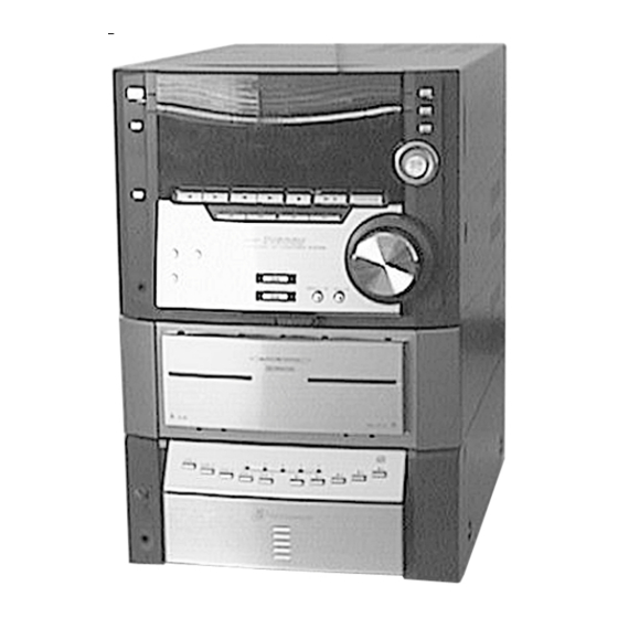
Page 1: Specifications
HCD-ZX30AV SERVICE MANUAL Canadian Model AEP Model UK Model E Model Australian Model • This set is the Amplifier, CD player, Tape Deck and Tuner section in MHC-ZX30AV. Dolby noise reduction manufactured under license from Model Name Using Similar Mechanism Dolby Laboratories Licensing Corporation. - Page 2 CRITIQUES POUR LA SÉCURITÉ DE FONCTIONNEMENT. NE COMPONENTS WITH SONY PARTS WHOSE PART NUMBERS REMPLACER CES COMPOSANTS QUE PAR DES PIÈSES SONY APPEAR AS SHOWN IN THIS MANUAL OR IN SUPPLEMENTS DONT LES NUMÉROS SONT DONNÉS DANS CE MANUEL OU PUBLISHED BY SONY.
-
Page 3: Table Of Contents
TABLE OF CONTENTS 1. GENERAL ·········································································· 5 MODEL IDENTIFICATION — BACK PANEL — 2. DISASSEMBLY ································································ 8 3. SERVICE MODE ···························································· 16 4. MECHANICAL ADJUSTMENTS ····························· 19 Parts No. 5. ELECTRICAL ADJUSTMENTS ······························· 19 6. DIAGRAMS 6-1. Circuit Boards Location ·············································· 24 6-2. - Page 4 This appliance is classified as a CLASS 1 LASER product. The CLASS 1 LASER PRODUCT MARKING is located on the rear exterior. Laser component in this product is capable of emitting radiation exceeding the limit for Class 1. The following caution label is located inside the unit. NOTES ON HANDLING THE OPTICAL PICK-UP BLOCK OR BASE UNIT The laser diode in the optical pick-up block may suffer electrostatic...
-
Page 5: General
SECTION 1 GENERAL LOCATION OF CONTROLS – Front Panel – 1 2 34 5 6 7 89 1 b button and indicator (TAPE A) wh Z indicator (DISC 5) 2 B button and indicator (TAPE A) wj Z indicator (DISC 4) 3 b button and indicator (TAPE B) wk Z indicator (DISC 3) wl Z indicator (DISC 2) - Page 6 – Rear Panel – q; qa 1 AM ANTENNA (75 Ω) terminals 2 FM ANTENNA (75 Ω) terminals 3 VIDEO IN jacks 4 MD IN jacks 5 MD OUT jacks 6 DVD IN jacks 7 WOOFER OUT jacks 8 CD DIGITAL OUT connector 9 FRONT SPEAKER terminals q;...
- Page 7 This section is extracted from instruction manual. Step 3: Setting the time Move the multi stick toward v or V repeatedly to set the hour. Move the multi stick toward B. You must set the time before using the timer The minute indication flashes.
-
Page 8: Disassembly
SECTION 2 DISASSEMBLY Note: Follow the disassembly procedure in the numerical order given. 3 Five screws (BVTT 3 × 8) 2-1. UPPER CASE 4 Upper case 1 Three screws (CASE3 TP2) 2 Three screws (CASE3 TP2) 2-2. FRONT PANEL SECTION 5 Connector 2 Wire (flat type) (15 core) - Page 9 2-3. BACK PANEL SECTION 4 Remove the back panel to direction of the arrow. 3 Eighteen screws 1 Wire (flat type) (BVTP 3 × 8) (13 core) or (15 core) 2 Connector 2-4. MAIN BOARD 1 One connector 6 Remove the MAIN board to direction of the arrow.
- Page 10 2-5. POWER TRANSFORMER (T902) 5 Four screws (BVTT 4 × 6) 3 Connector 1 Connector 4 Power cord 6 Power transforme (T902) 2 Connector 2-6. FRONT AMP BOARD 9 Two screws (BVTP 3 × 8) 0 Heat sink 6 Two screws (BVTP 3 ×...
- Page 11 2-7. CD MECHANISM DECK (CDM53F-K2BD38) 5 Remove the CD mechanism deck section. 4 Four screws 3 Chassis (BVTP 3 × 8) 2 Two screws (BVTP 3 × 8) 1 Three screws (BVTP 3 × 8) 2-8. TAPE MECHANISM DECK (TCM-230AWR12) 3 Remove the tape mechanism deck section.
- Page 12 2-9. CD BASE UNIT (BU-K2BD38) 5 CD base unit (BU-K2BD38) 4 Compression spring 2 Compression spring (black) (sliver) 1 Two screws 3 Two screws (PTPWH M2.6) (PTPWH M2.6) 2-10. FITTING BASE (GUIDE) ASSY, BRACKET (CHASSIS) AND MAGNET ASSY 8 Four screws (BVTP M2.6) 6 Bracket (chassis)
- Page 13 2-11. TRAY (SUB) 1 Rotating the pulley (LD), shift the slider (selection) in the arrow A direction. 2 Rotating the pulley (mode) in the arrow direction, adjust the tray (sub) to be removed. 3 Rotating the pulley (LD), shift the slider (selection) in the arrow B direction. 4 Rotating the pulley (mode) in the arrow direction, remove the tray (sub) to be removed.
- Page 14 2-13. GEARS INSTALLATION 3 Gear (gear B) Portion A Adjust the gear (gear B) with the portion A as shown. 1 Slide the slider (u/d) fully in the arrow direction. 4 Gear (gear A) 2 Gear (U/D slider) Gear Slider (U/D) gear Linearly (gear B) Adjust so as to be aligned with...
- Page 15 2-15. STOCKER SECTION INSTALLATION 2 Portion A of tray (sub) Hook the portion A of tray (sub) 1 Stocker section to the slider (selection). Portion A Sticking of of tray (sub) slider (selection) 3 Two step screws 3 Two step screws 2-16.
-
Page 16: Service Mode
SECTION 3 SERVICE MODE [MC Cold Reset] [Change-over of AM Tuner Step between 9 kHz and • The cold reset clears all data including preset data stored in the 10 kHz] RAM to initial conditions. Execute this mode when returning •... - Page 17 [MC Test Mode] [Aging Mode] • This mode is used to check operations of the respective sections During the aging mode, both the CD player and tape deck are of Amplifier, Tuner, CD and Tape. executed together. • If an error occurs: Procedure: Aging stops, and the error state is displayed on the fluorescent Press the three buttons of x , DISPLAY and DISC 3...
- Page 18 [Error History Display Mode] Mode which enables the history of error occurring in the CD player to be checked. Execute this mode after ending the aging mode. Procedure: Press the ?/1 button to turn the set ON. x , DISPLAY , and Z1 Press the three buttons simultaneously.
-
Page 19: Mechanical Adjustments
SECTION 4 SECTION 5 MECHANICAL ADJUSTMENTS ELECTRICAL ADJUSTMENTS Precaution DECK SECTION 0 dB=0.775V Clean the following parts with a denatured alcohol- moistened swab: Demagnetize the record/playback head with a head record/playback heads pinch rollers demagnetizer. erase head rubber belts Do not use a magnetized screwdriver for the adjustments. capstan idlers After the adjustments, apply suitable locking compound to... - Page 20 Tape Speed Adjustment (Deck A) Mode: Playback Note: Set the test mode using the following method and begin Test tape tape speed adjustment. P-4-A100 In the test mode, the speed will switch to double speed or Oscilloscope (10 kHz, –10 dB) Pin 1 normal speed each time the HI-SPEED DUB button is pressed.
- Page 21 Record Bias Adjustment (Deck B) Record Level Adjustment (Deck B) Procedure: Procedure: INTRODUCTION INTRODUCTION When set to the test mode performed in Tape Speed Adjustment, When set to the test mode performed in Tape Speed Adjustment, when the tape is rewound after recording, the “REC memory when the tape is rewound after recording, the “REC memory mode”...
- Page 22 Note : Clear RF signal waveform means that the shape “ ◊ ” can be clearly CD SECTION distinguished at the center of the waveform. Note : RF signal waveform 1. CD Block is basically designed to operate without adjustment. VOLT/DIV : 200mV Therefore, check each item in order given.
-
Page 23: Diagrams
SECTION 6 DIAGRAMS NOTE FOR PRINTED WIRING BOARDS AND SCHEMATIC DIAGRAMS (In addition to this, the necessary note is printed in each block) Note on Printed Wiring Board: Note on Schematic Diagram: • X : parts extracted from the component side. •... -
Page 24: Circuit Boards Location
6-1. CIRCUIT BOARDS LOCATION TRANS board SUB TRANS board TUNER unit PANEL board HP board SURR AMP board FRONT AMP board SUB PANEL board MIC board MAIN board CD SWITCH board CLAMP MOTOR board BD board INT/COUNT SW board SENSOR 2 board IN SW board LEAF SW board CONNECTOR board... -
Page 25: Block Diagrams
HCD-ZX30AV 6-2. BLOCK DIAGRAMS PB EQ DECK-A PB(L) RV311 TC REC-L MAIN TUNER/CD/DECK SECTION IC611 LEVEL SECTION (Page 26) HP101 DOLBY HEAD PB EQ TC PB-L MAIN R-CH PB(L) SECTION RV301 LEVEL IC601 (Page 26) REC/PB SWITCH DECK-B IC602 • RCH is omitted •... - Page 26 HCD-ZX30AV MAIN SECTION EXCEPT CND,AEP,UK,G,AED,CIS MODEL R CH POWER AMP J1691 IC801 HEADPHONS MUTE Q821 FAN DRIVE CND,AEP,UK,G,AED,CIS INPUT SELECT/ Q941,942 MODEL GRAPHIC EQ CONT/ ELECTRICAL VOLUME POWER AMP IC101 IC801 TM801 ST-L TUNER INA2 OUT2 SECTION (Page 25) RY881...
- Page 27 HCD-ZX30AV DISPLAY/POWER SECTION DISPLAY CONTROL IC701 FL701 SPA SIG MAIN BPF1 FLOURESCENT SECTION INDICATOR TUBE SPEANA BPF2 (Page 26) BPF3 IC704 MIC SIG MAIN BPF4 SECTION BPF5 (Page 26) BPF6 IC1601 IC1601 J1601 T902 MIC 1 IC905 MAIN TRANS DRIVER...
-
Page 28: Printed Wiring Board
HCD-ZX30AV • See page 24 for Circuit Boards Location. 6-3. PRINTED WIRING BOARD BD Board • Semiconductor Location Ref. No. Location IC101 IC102 IC103 TP(TE0) (VC) Q101 TP(FE0) (RF) TP(FE1) TP(AGC CON) TP(D GND) (XPCK) (Page 35) -
Page 29: Schematic Diagram
HCD-ZX30AV 6-4. SCHEMATIC DIAGRAM BD Board • See page 42 for Waveforms. • See page 50 for IC Block Diagrams. (Page 37) • Voltages and waveforms are dc with respect to ground under no-signal conditions. no mark : CD STOP... -
Page 30: Printed Wiring Boards
HCD-ZX30AV • See page 24 for Circuit Boards Location. 6-5. PRINTED WIRING BOARDS SENSOR/MOTOR Section TO MAIN BOARD (Page 35) MAIN BOARD (Page 35) -
Page 31: Schematic Diagram
HCD-ZX30AV 6-6. SCHEMATIC DIAGRAM SENSOR/MOTOR Section MAIN BOARD (Page 37) MAIN BOARD (Page 37) • Voltages are dc with respect to ground under no-signal conditions. no mark : CD STOP... -
Page 32: Audio Board
HCD-ZX30AV • See page 24 for Circuit Boards Location. 6-7. PRINTED WIRING BOARD AUDIO Board (Page 35) • Semiconductor Location Ref. No. Location IC601 IC602 IC611 Q621 Q622 Q623... -
Page 33: Schematic Diagram
HCD-ZX30AV 6-8. SCHEMATIC DIAGRAM AUDIO Board • See page 50 for IC Block Diagrams. MAIN BOARD (Page 36) JW20 JW16 The components identified by Les composants identifiés par mark 0 or dotted line with mark une marque 0 sont critiques 0 are critical for safety. -
Page 34: Leaf Sw Board
HCD-ZX30AV • See page 24 for Circuit Boards Location. 6-9. PRINTED WIRING BOARD LEAF SW Board PLAY PLAY (Page 35) 6-10. SCHEMATIC DIAGRAM LEAF SW Board (Page 36) • Voltages are dc with respect to ground under no-signal conditions. no mark : TAPE PLAY... -
Page 35: Main Board
HCD-ZX30AV 6-11. PRINTED WIRING BOARD MAIN Board • See page 24 for Circuit Boards Location. • Semiconductor Location EA,MY,SP,KR, TH MODEL Ref. No. Location (Page 42) (Page 46) : AEP,UK,G,AED, D101 B-10 CIS MODEL EA,MY,SP,KR, D102 C-10 TH MODEL D181... -
Page 36: Main Board (1/2)
HCD-ZX30AV • See page 42 for Waveforms. 6-12. SCHEMATIC DIAGRAM MAIN Board (1/2) • See page 51 for IC Pin Function. CN301 TEST PIN FUNCTION • Voltages and waveforms are dc with respect to ground under no-signal (detuned) conditions. no mark : TUNER (FM/AM) -
Page 37: Schematic Diagram
HCD-ZX30AV 6-13. SCHEMATIC DIAGRAM MAIN Board (2/2) –9.5 –7.9 –7.9... -
Page 38: Panel Board
HCD-ZX30AV • See page 24 for Circuit Boards Location. 6-14. PRINTED WIRING BOARD PANEL Board (Page 48) • Semiconductor Location Ref. No. Location D601 D602 D603 D604 D661 D662 D663 D664 D665 D691 D755 D756 D761 D762 EA,MY,SP, KR,TH MODEL... -
Page 39: Schematic Diagram
HCD-ZX30AV 6-15. SCHEMATIC DIAGRAM PANEL Board • See page 42 for Waveforms. • See page 50 for IC Block Diagrams. • See page 53 for IC Pin Function. PIN FUNCTION • Voltages are dc with respect to ground un- no-signal (detuned) conditions. -
Page 40: Sub Panel Board
HCD-ZX30AV • See page 24 for Circuit Boards Location. 6-16. PRINTED WIRING BOARD SUB PANEL Board • Semiconductor Location Ref. No. Location D605 D606 D607 D608 D609 D610 D611 D612 D613 D617 D618 D652 Q605 Q607 Q609 Q611 Q613 Q617... -
Page 41: Schematic Diagram
HCD-ZX30AV 6-17. SCHEMATIC DIAGRAM SUB PANEL Board • Voltages are dc with respect to ground under no-signal (detuned) conditions. no mark : FM... -
Page 42: Waveforms
HCD-ZX30AV • See page 24 for Circuit Boards Location. 6-18. WAVEFORMS 6-19. PRINTED WIRING BOARD MIC Board – BD BOARD – – MAIN BOARD – IC401 qa IC101 yj IC101 ra STOP MODE CD PLAY MODE CD PLAY MODE approx 200mVp-p 6.4Vp-p... -
Page 43: Schematic Diagram
HCD-ZX30AV 6-20. SCHEMATIC DIAGRAM MIC Board • Voltages are dc with respect to ground under no-signal (detuned) conditions. no mark : FM... -
Page 44: Printed Wiring Board
HCD-ZX30AV • See page 24 for Circuit Boards Location. 6-21. PRINTED WIRING BOARD FRONT AMP Board • Semiconductor (Page 35) (Page 35) Location Ref. No. Location D801 D802 D821 D831 D851 D871 D881 D911 D951 D961 D962 D963 D981 D982... -
Page 45: Schematic Diagram
HCD-ZX30AV 6-22. SCHEMATIC DIAGRAM FRONT AMP Board • Voltages are dc with respect to ground under no-signal (detuned) conditions. no mark : FM... -
Page 46: Printed Wiring Board
HCD-ZX30AV • See page 24 for Circuit Boards Location. 6-23. PRINTED WIRING BOARD SURROUND AMP Board (Page 44) • Semiconductor Location Ref. No. Location D1001 D1002 D1051 D1061 D1062 D1081 IC1001 Q1001 Q1051 Q1061 Q1062 Q1063 Q1064 Q1081 Q1091 Q1092... -
Page 47: Schematic Diagram
HCD-ZX30AV 6-24. SCHEMATIC DIAGRAM SURROUND AMP Board... -
Page 48: Printed Wiring Boards
HCD-ZX30AV • See page 24 for Circuit Boards Location. 6-25. PRINTED WIRING BOARDS TRANS/SUB TRANS Boards • Semiconductor Location CND MODEL Ref. No. Location D901 F914 : AEP,UK,G,AED,CIS,CND MODEL JW914 : EXCEPT AEP,UK,G,AED,CIS,CND MODEL D902 D903 D904 F915 : AEP,UK,G,AED,CIS,CND MODEL... -
Page 49: Schematic Diagram
HCD-ZX30AV 6-26. SCHEMATIC DIAGRAM TRANS/SUB TRANS Boards AEP,UK,G,AED,CIS, CND MODEL EXCEPT AEP,UK,G, AED,CIS,CND MODEL EXCEPT AEP,UK,G, AED,CIS,CND MODEL AEP,UK,G,AED, CIS,CND MODEL AEP,UK,G,AED,CIS,MX, AUS,TH,KR MODEL AEP,UK,G,AED,CIS, MX,AUS MODEL JW924 MX,CND MODEL E,EA,MY,SP,AR MODEL F911, JW924 The components identified by Les composants identifiés par... -
Page 50: Ic Block Diagrams
HCD-ZX30AV 6-27. IC BLOCK DIAGRAMS – BD Board – IC103 CXA2568M-T6 IC101 CXD2587Q HOLD APC PD AMP LC/PD APC LD AMP – LD ON – ERROR DIGITAL CORRECTOR ASYMMETRY DIGITAL – CORRECTION – OPERATIONAL LRCK AMPLIFIER HOLD SW ANALOG SWITCH... -
Page 51: Ic Pin Function Description
6-28. IC PIN FUNCTION DESCRIPTION • MAIN BOARD IC401 M30620MCA-A35FP Pin No. Pin Name Description CD_DATA BD data out CD_CLK BD clock BD LAT AC CUT AC cut ON (L) / OFF (H) Check CAN'T USE Not used SQ_DATA_IN BD sub-Q Data in SQ_CLK BD sub-Q Clock BYTE... - Page 52 Pin No. Pin Name Description STEREO Stereo IN (L) / OFF (H) ST-MUTE Tuner mute AMS-IN AMS signal in (L) / OFF (H) TC-MUTE TC line mute on (H) / OFF (L) R/PB/PAS REC (L) / PB ( Z) / Pass (H) NR-ON/OFF Dolby NR ON (H) / OFF (L) REC-MUTE...
- Page 53 • PANEL BOARD IC701 TMP88CS77AF-1A84 (FLUORESCENT INDICATOR TUBE DRIVE, LED DRIVE, KET CONTROL) Pin No. Pin Name Description LED SEL LED select switch( for dynamic) 2 to 12 LED0 to LED10 LED (high active) STANDBY LED Standby LED TIMER LED Timer SEL LED VOLUME A Volume A...
-
Page 54: Exploded Views
SECTION 7 EXPLODED VIEWS NOTE: • -XX, -X mean standardized parts, so they may • Abbreviation The components identified by mark 0 or have some differences from the original one. CND : Canadian model. dotted line with mark 0 are critical for safety. •... - Page 55 7-2. FRONT PANEL SECTION not supplied supplied EA, MY, SP, not supplied supplied KR, TH supplied TCM-230PWR12 supplied supplied Ref. No. Part No. Description Remarks Ref. No. Part No. Description Remarks 4-226-734-01 BUTTON (A), EJECT 4-226-713-01 CURSOR 4-226-735-01 BUTTON (B), EJECT A-4473-239-A SUB PANEL BOARD, COMPLETE (TH) 4-226-537-01 SPRING (TC EJECT), COIL A-4428-628-A SUB PANEL BOARD, COMPLETE (EXCEPT TH)
-
Page 56: Chassis Section
7-3. CHASSIS SECTION EA, MY, SP CND, E, MX, TH AEP, UK, G, AED, CIS, EA, MY, SP, KR CDM53F-K2BD38 T902 supplied supplied supplied supplied Ref. No. Part No. Description Remarks Ref. No. Part No. Description Remarks 4-965-822-01 FOOT A-4428-632-A SURR AMP BOARD, COMPLETE 1-773-041-11 WIRE (FLAT TYPE) (17 CORE) (AEP,UK,G,AED,CIS) 1-792-794-11 WIRE (FLAT TYPE) (19 CORE) - Page 57 7-4. CD MECHANISM DECK SECTION-1 (CDM53F-K2BD38) M702 Ref. No. Part No. Description Remarks Ref. No. Part No. Description Remarks 4-218-253-11 SCREW (M2.6), +BTTP 4-214-129-01 COVER 1-671-508-11 LOAD MOTOR BOARD 4-211-235-01 BELT (COMMUNICATION) 4-220-261-01 GEAR (EJECT) 4-211-236-01 BELT (LOADING) 1-671-502-11 INT/COUNT SW BOARD 4-211-231-01 PULLEY (MODE) 1-671-504-11 SENSOR BOARD 4-211-214-01 PULLEY (LD)
- Page 58 7-5. CD MECHANISM DECK SECTION-2 (CDM53F-K2BD38) not supplied not supplied S707 not supplied M701 Ref. No. Part No. Description Remarks Ref. No. Part No. Description Remarks 4-985-672-01 SCREW (+PTPWH M2.6), FLOATING 1-671-507-11 CLAMP MOTOR BOARD 4-220-933-01 INSULATOR 4-211-221-01 GEAR (LD MOVABLE) 4-211-212-51 TRAY (SUB) 4-211-217-01 GEAR (SELECTION) 4-213-482-02 CHASSIS (MODE A)
- Page 59 7-6. TAPE MECHANISM DECK SECTION-1 (TCM-230AWR12) HP101 HRPE101 Ref. No. Part No. Description Remarks Ref. No. Part No. Description Remarks 3-376-464-11 SCREW(+PTT 2.6X6),GROUND POINT 3-017-366-01 BASE (PINCH LEVER REV) 3-911-116-42 RIVET, PUSH 3-016-567-02 SPRING (CASSETTE), LEAF 3-016-574-01 SPRING (HEAD), TENSION A-2007-845-A AUDIO BOARD, COMPLETE X-3374-156-4 PINCH LEVER (REV) ASSY HP101...
- Page 60 7-7. TAPE MECHANISM DECK SECTION-2 (TCM-230AWR12) Ref. No. Part No. Description Remarks Ref. No. Part No. Description Remarks X-4952-881-1 CHASSIS ASSY, MAIN A-2007-838-A LEAF SW BOARD, COMPLETE 3-041-946-01 BELT (CAPSTAN B) 4-228-450-01 SPRING (REVERSE SLIDER),TORSION 4-227-239-01 BELT (CAPSTAN C) 3-019-208-01 WASHER, STOPPER 3-016-568-01 BRACKET (MOTOR) 3-027-453-01 SPRING (GROUND), TENSION X-3378-040-1 FLYWHEEL (A-FWD) ASSY...
- Page 61 SECTION 8 AUDIO ELECTRICAL PARTS LIST NOTE: • Due to standardization, replacements in the • Abbreviation • SEMICONDUCTORS parts list may be different from the parts CND : Canadian model. In each case, u: µ, for example: specified in the diagrams or the components : German model.
- Page 62 AUDIO Ref. No. Part No. Description Remarks Ref. No. Part No. Description Remarks R612 1-249-409-11 CARBON 1/4W F C167 1-163-237-11 CERAMIC CHIP 27PF 5.00% 50V 0 R621 1-212-851-00 FUSIBLE 1/4W C168 1-163-235-11 CERAMIC CHIP 22PF 5.00% 50V 0 R622 1-212-851-00 FUSIBLE 1/4W C171 1-163-009-11 CERAMIC CHIP...
- Page 63 CD SW CONNECTOR CLAMP MOTOR FRONT AMP Ref. No. Part No. Description Remarks Ref. No. Part No. Description Remarks R173 1-216-077-91 RES-CHIP 1/10W < TRANSISTOR > R181 1-216-078-00 RES-CHIP 1/10W R182 1-216-073-00 METAL CHIP 1/10W Q701 8-729-029-66 TRANSISTOR RT1N141S-TP R183 1-216-077-91 RES-CHIP 1/10W <...
- Page 64 FRONT AMP Ref. No. Part No. Description Remarks Ref. No. Part No. Description Remarks C812 1-162-306-11 CERAMIC 0.01uF 30.00% 16V < CONNECTOR > C821 1-107-721-11 ELECT 4.7uF 20.00% 100V C822 1-107-717-11 ELECT 47uF 20.00% 50V CN801 1-691-768-11 PLUG (MICRO CONNECTOR) 6P C831 1-136-165-00 MYLAR 0.1uF...
- Page 65 FRONT AMP Ref. No. Part No. Description Remarks Ref. No. Part No. Description Remarks Q894 8-729-119-78 TRANSISTOR 2SC2785TP-HFE R857 1-249-431-11 CARBON 1/4W Q895 8-729-119-78 TRANSISTOR 2SC2785TP-HFE R858 1-249-441-11 CARBON 100K 1/4W Q896 8-729-119-78 TRANSISTOR 2SC2785TP-HFE R859 1-260-076-11 CARBON 1/2W Q897 8-729-119-78 TRANSISTOR 2SC2785TP-HFE R861 1-260-076-11 CARBON...
- Page 66 IN SW INT/COUNT SW LEAF SW LOAD MOTOR MAIN Ref. No. Part No. Description Remarks Ref. No. Part No. Description Remarks 1-676-971-11 HP BOARD R1006 1-247-864-11 CARBON 1/4W R1007 1-247-780-00 CARBON 1/4W ********* R1008 1-249-417-11 CARBON 1/4W F < CAPACITOR > <...
- Page 67 MAIN Ref. No. Part No. Description Remarks Ref. No. Part No. Description Remarks < CAPACITOR > C175 1-104-665-11 ELECT 100uF 20.00% 10V C181 1-109-889-11 ELECT 20.00% 50V C103 1-126-960-11 ELECT 20.00% 50V C192 1-163-001-11 CERAMIC CHIP 220PF C107 1-136-157-00 MYLAR 0.022uF 5.00% 50V (AEP,UK,G,AED,CIS)
- Page 68 MAIN Ref. No. Part No. Description Remarks Ref. No. Part No. Description Remarks C251 1-126-963-11 ELECT 4.7uF 20.00% 50V C353 1-136-165-00 MYLAR 0.1uF 5.00% 50V C252 1-126-934-11 ELECT 220uF 20.00% 16V C354 1-136-165-00 MYLAR 0.1uF 5.00% 50V C253 1-126-934-11 ELECT 220uF 20.00% 16V C355...
- Page 69 MAIN Ref. No. Part No. Description Remarks Ref. No. Part No. Description Remarks < CONNECTOR > < IC > CN103 1-785-316-41 PIN, CONNECTOR (STRAIGHT) 4P IC101 8-759-663-66 IC M61502FP (EA,MY,SP,KR,TH) IC201 8-759-571-51 IC M62464FP CN304 1-784-778-11 CONNECTOR, FFC 17P IC203 8-759-636-55 IC M5218AFP-T1 CN305 1-784-776-11 CONNECTOR, FFC 15P...
- Page 70 MAIN Ref. No. Part No. Description Remarks Ref. No. Part No. Description Remarks Q921 8-729-052-12 TRANSISTOR ZSB1568 JR45 1-216-295-91 SHORT 0 Q922 8-729-900-53 TRANSISTOR DTC114EKA-T146 JR47 1-216-296-91 SHORT 0 Q941 8-729-111-29 TRANSISTOR 2SD1616A-TP-LK JR48 1-216-296-91 SHORT 0 Q942 8-729-600-22 TRANSISTOR 2SA1235TP-1EF JR49 1-216-296-91 SHORT 0 JR50...
- Page 71 MAIN Ref. No. Part No. Description Remarks Ref. No. Part No. Description Remarks R203 1-216-073-00 METAL CHIP 1/10W R312 1-216-102-00 RES-CHIP 160K 1/10W R204 1-216-057-00 METAL CHIP 2.2K 1/10W R313 1-216-097-91 RES-CHIP 100K 1/10W R205 1-216-097-91 RES-CHIP 100K 1/10W R315 1-216-073-00 METAL CHIP 1/10W R206...
- Page 72 MAIN Ref. No. Part No. Description Remarks Ref. No. Part No. Description Remarks R423 1-216-025-91 RES-CHIP 1/10W R494 1-216-073-00 METAL CHIP 1/10W R424 1-216-025-91 RES-CHIP 1/10W (EA) R425 1-216-025-91 RES-CHIP 1/10W R494 1-216-053-00 METAL CHIP 1.5K 1/10W R426 1-216-025-91 RES-CHIP 1/10W (MY,SP,KR,AUS,TH) R428...
- Page 73 OUT SW PANEL Ref. No. Part No. Description Remarks Ref. No. Part No. Description Remarks C1611 1-126-964-11 ELECT 10uF 20.00% 50V C714 1-162-286-31 CERAMIC 220PF C1612 1-162-306-11 CERAMIC 0.01uF 30.00% 16V C715 1-162-286-31 CERAMIC 220PF C1613 1-162-306-11 CERAMIC 0.01uF 30.00% 16V C716 1-162-286-31 CERAMIC 220PF...
- Page 74 PANEL Ref. No. Part No. Description Remarks Ref. No. Part No. Description Remarks < IC > R713 1-249-441-11 CARBON 100K 1/4W R714 1-249-441-11 CARBON 100K 1/4W IC701 8-759-664-40 IC TMP88CS77AF-1A84 R715 1-249-441-11 CARBON 100K 1/4W IC702 8-749-011-05 IC GP1U28X R716 1-249-441-11 CARBON 100K 1/4W...
- Page 75 PANEL SENSOR SENSOR2 SUB PANEL Ref. No. Part No. Description Remarks Ref. No. Part No. Description Remarks R816 1-249-437-11 CARBON 1/4W D618 8-719-058-64 DIODE SEL5823A-TP15 (GROOVE) R817 1-249-437-11 CARBON 1/4W D652 8-719-056-13 DIODE SML79423C-TP15 < SWITCH > < EARTH > S601 1-762-875-21 SWITCH, KEYBOARD (POWER) * EPT701 1-537-738-21 TERMINAL, EARTH...
- Page 76 SUB PANEL SUB TRANS SURR AMP Ref. No. Part No. Description Remarks Ref. No. Part No. Description Remarks < SWITCH > A-4428-622-A SURR AMP BOARD, COMPLETE (CND) ************************** S607 1-762-875-21 SWITCH, KEYBOARD (HI DUB) A-4428-643-A SURR AMP BOARD, COMPLETE S608 1-762-875-21 SWITCH, KEYBOARD (REC PAUSE) (E,EA,MY,SP,KR,MX,AR,AUS) S609...
- Page 77 SURR AMP TRANS Ref. No. Part No. Description Remarks Ref. No. Part No. Description Remarks < TRANSISTOR > R1094 1-249-433-11 CARBON 1/4W Q1001 8-729-140-84 TRANSISTOR 2SC1841TP-PAFAEA < RELAY > Q1041 8-729-119-78 TRANSISTOR 2SC2785TP-HFE (AEP,UK,G,AED,CIS) RY1061 1-515-920-11 RELAY (24V) Q1051 8-729-140-84 TRANSISTOR 2SC1841TP-PAFAEA RY1062 1-515-920-11 RELAY (24V) Q1061 8-729-140-82 TRANSISTOR 2SA988TP-PAFAEA...
- Page 78 HCD-ZX30AV Ref. No. Part No. Description Remarks Ref. No. Part No. Description Remarks MISCELLANEOUS ************** HARDWARE LIST ************** ************** 1-769-980-11 WIRE(FLAT TYPE) (13 CORE) (CND,E,EA,MY,SP,KR,TH,MX,AR,AUS) 7-685-871-01 SCREW +BVTT 3X6 (S) 1-773-013-11 WIRE(FLAT TYPE) (15 CORE)(190mm) 7-685-146-11 SCREW +P3X8 TYPE2 NON-SLIT...