Advertisement
SERVICE MANUAL
Ver 1.4 2004.09
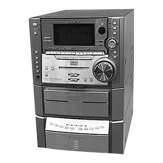
HCD-ZX70DVD is the Amplifier, DVD/CD
player, Tape Deck and Tuner section in
MHC-ZX70DVD.
This stereo system is equipped with the Dolby B-type noise
reduction system*.
* Manufactured under license from Dolby Laboratories
Licensing Corporation.
DOLBY and the double-D symbol ; are trademarks of
Dolby Laboratories Licensing Corporation.
This system incorporates Dolby* Digital and Pro Logic
Surround.
* Manufactured under license from Dolby Laboratories.
"Dolby", "AC-3", "Pro Logic" and the double-D symbol ;
are trademarks of Dolby Laboratories.
Confidential unpublished Works. © 1992-1997 Dolby
Laboratories, Inc. All rights reserved.
Amplifier section
AUDIO POWER SPECIFICATIONS:
(U.S.A. model only)
POWER OUTPUT AND TOTAL HARMONIC
DISTORTION:
with 8 ohm loads both channels driven, from 120-
10,000 Hz; rates 90 watts per channel minimum RMS
power, with no more than 10% total harmonic
distortion from 250 milliwatts to rated output.
Total harmonics distortion
Less than 0.07%
(8 ohms at 1 kHz, 50 W)
Center Speaker:
Continuous RMS power output
40 watts
(8 ohms at 1 kHz,
10% THD)
Rear Speaker:
Continuous RMS power output
40 + 40 watts
(8 ohms at 1 kHz,
10% THD)
Sony Corporation
9-929-264-15
2004I05-1
Audio Group
© 2004.09
Published by Sony Engineering Corporation
HCD-ZX70DVD
Model Name Using Similar Mechanism
DVD Mechanism Type
DVD
Section
Base Unit Name
Optical Pick-up Name
Model Name Using Similar Mechanism
TAPE
Section
Tape Transport Mechanism Type
SPECIFICATIONS
Canadian model:
Front Speaker:
Continuous RMS power output
100 + 100 watts
(8 ohms at 1 kHz,
10% THD)
Total harmonics distortion
Less than 0.07%
(8 ohms at 1 kHz, 50 W)
Center Speaker:
Continuous RMS power output
40 watts
(8 ohms at 1 kHz,
10% THD)
Rear Speaker:
Continuous RMS power output
40 + 40 watts
(8 ohms at 1 kHz,
10% THD)
European model:
Front Speaker:
DIN power output (rated) 80 + 80 watts
(8 ohms at 1 kHz, DIN)
COMPACT DISC DECK RECEIVER
US Model
Canadian Model
AEP Model
UK Model
E Model
Australian Model
Chinese Model
NEW
CDM53J-DVBU1
DVBU1
KHM-220AAA
HCD-ZX30AV
TCM-230AWR12
Continuous RMS power output (reference)
100 + 100 watts
(8 ohms at 1 kHz,
10% THD)
Music power output (reference)
170 + 170 watts
(8 ohms at 1 kHz,
10% THD)
Center Speaker:
DIN power output (rated) 30 watts
(8 ohms at 1 kHz, DIN)
Continuous RMS power output (reference)
40 watts
(8 ohms at 1 kHz,
10% THD)
Music power output (reference)
60 watts
(8 ohms at 1 kHz,
10% THD)
– Continued on next page –
Advertisement
Chapters

Related Manuals for Sony HCD-ZX70DVD


Summary of Contents for Sony HCD-ZX70DVD
-
Page 1: Specifications
AEP Model UK Model E Model Australian Model Chinese Model HCD-ZX70DVD is the Amplifier, DVD/CD player, Tape Deck and Tuner section in MHC-ZX70DVD. This stereo system is equipped with the Dolby B-type noise Model Name Using Similar Mechanism reduction system*. - Page 2 Frequency response 40 – 13,000 Hz ( 3 dB), Continuous RMS power output (reference) (DOLBY NR OFF) using Sony TYPE I cassette 40 + 40 watts 40 – 14,000 Hz ( 3 dB), (8 ohms at 1 kHz, using Sony TYPE II cassette...
-
Page 3: Table Of Contents
OPERATION. REPLACE THESE COMPONENTS WITH DE FONCTIONNEMENT. NE REMPLACER CES COM- SONY PARTS WHOSE PART NUMBERS APPEAR AS POSANTS QUE PAR DES PIÈCES SONY DONT LES SHOWN IN THIS MANUAL OR IN SUPPLEMENTS PUB- NUMÉROS SONT DONNÉS DANS CE MANUEL OU LISHED BY SONY. - Page 4 SAFETY CHECK-OUT CAUTION After correcting the original service problem, perform the follow- Use of controls or adjustments or performance of procedures ing safety check before releasing the set to the customer: other than those specified herein may result in hazardous ra- Check the antenna terminals, metal trim, “metallized”...
-
Page 5: Servicing Notes
SECTION 1 SERVICING NOTES MODEL IDENTIFICATION NOTES ON HANDLING THE OPTICAL PICK-UP – Back Panel – BLOCK OR BASE UNIT The laser diode in the optical pick-up block may suffer electro- PART No. static break-down because of the potential difference generated by the charged electrostatic load, etc. - Page 6 NOTE ON TEMPERATURE OF HEAT SINK heat sink Heat sink gets heated up to a high temperature. Be careful not to get burnt. SERVICE POSITION In checking the DVD block, prepare jig (extension cable J-2501-198-A: 700 mm 17 cores). IF board MB board CONNECT board Connect jig (extension cable J-2501-198-A)
-
Page 7: General
SECTION 2 GENERAL LOCATION OF CONTROLS qf MODE SELECT button qg PUSH ENTER multi stick • Front View qh TITLE button 456 789 q; qa qj DVD MENU button qk m, M buttons ql ., > buttons w; VOLUME knob wa GROOVE button and indicator ws GROOVE-EX button and indicator wd Z B button... - Page 8 This section is extracted from instruction manual.
-
Page 9: Disassembly
SECTION 3 DISASSEMBLY • This set can be disassembled in the order shown below. UPPER CASE (Page 10) FRONT PANEL SECTION (Page 10) TAPE MECHANISM DECK BACK PANEL SECTION (TCM-230AWR12) (Page 11) (Page 17) MAIN BOARD (Page 11) POWER TRANSFORMER IF BOARD (T902) (Page 12) (Page 12) - Page 10 Note: Follow the disassembly procedure in the numerical order given. UPPER CASE 4 upper case 3 five screws (BVTT 3 1 three screws (CASE3 TP2) 2 three screws (CASE3 TP2) FRONT PANEL SECTION 5 connector (CN914) 2 wire (flat type) (15 core) (CN305) 1 connector (CN504)
- Page 11 BACK PANEL SECTION 1 wire (flat type) (13 core) or(15 core) 3 connector (CN502) (CN201) 7 Remove the back panel to direction of the arrow. 2 connector (CN901) 4 three screws (BVTP 3 2 connector (CN902) 4 screw (BVTP 3 2 connector 4 fifteen screws (CN903)
- Page 12 POWER TRANSFORMER (T902) 3 four screws (BVTP 4 1 connector 4 Power transforme (T902) (CN801) 2 connector (CN913) IF BOARD 2 connector (CN13) 3 screws (BVTP 3 2 connector (CN11) 4 IF board 1 wire (flat type) (23 core) (CN5) 1 wire (flat type) (13 core) (CN7) 1 wire (flat type) (17 core)
- Page 13 FRONT AMP BOARD 9 two screws (BVTP 3 0 heat sink 6 two screws 1 connector (BVTP 3 (CN1002) 8 front amp board 2 two screws (BVTP 3 7 two screws (BVTP 3 5 surrund amp board 4 bracket 3 two screws (BVTP 3 3 screw MB BOARD...
- Page 14 DVD MECHANISM DECK (CDM5J-DVBU) 1 four screws 2 Remove the DVD mechanism (BVTP 3 deck section. FITTING BASE (GUIDE) ASS’Y, BRACKET (CHASSIS) AND MAGNET ASS’Y 8 four screws (BTTP M2.6) 6 Bracket (chassis) 2 four screws (BTTP M2.6) 4 two screws (BTTP M2.6) 7 connector (CN710)
- Page 15 MAGNET ASS’Y, DVD BASE UNIT (DVBU1) 2 four screws (BVTP M2.6) 3 magnet ass’y 1 connector (CN710) 5 DVD base unit (DVBU1) 4 two screws (PTPWH M2.6) OPTICAL PICK-UP (KHM-220AAA), TK BOARD 5 three step screws 8 optical pick-up (KHM-220AAA) 7 insulator 7 insulator 7 insulator...
- Page 16 TRAY (SUB) 1 Rotating the pulley (LD), shift the slider (selection) in the arrow A direction. 2 Rotating the pulley (mode) in the arrow direction, adjust the tray (sub) to be removed. 3 Rotating the pulley (LD), shift the slider (selection) in the arrow B direction. 4 Rotating the pulley (mode) in the arrow direction, remove the tray (sub) to be removed.
- Page 17 TAPE MECHANISM DECK (TCM-230AWR12) 3 Remove the tape mechanism deck section. 1 two screws (BVTP 3 2 two screws (BVTP 3 CABLE SETTING When connecting the cable from PANEL board (CN704) to CD board (CN754), set it as shown in the figure. FRONT PANEL - BACK VIEW - CN704...
-
Page 18: Assembly
SECTION 4 ASSEMBLY GEARS INSTALLATION (Page 18) SLIDER (SELECTION) INSTALLATION (Page 19) STOCKER SECTION INSTALLATION (Page 19) CHASSIS (MOLD B) SECTION INSTALLATION (Page 20) Note: Follow the assembly procedure in the numerical order given. GEARS INSTALLATION 3 gear (gear B) portion A Adjust the gear (gear B) with the portion A as shown. - Page 19 SLIDER (SELECTION) INSTALLATION 6 two screws (PTPWH M2.6) 2 gear (chuking) rotary encoder 5 washer 4 compression spring 7 Insert the slider (selection) into the portion A. Align with the slot of rotary encoder. portion A 3 convex portion of slider (selection) Gear (chuking) 1 rotary encoder...
- Page 20 CHASSIS (MOLD B) SECTION INSTALLATION 3 three screws (BVTP M2.6) 2 Insert the gear (eject0 1 Insert the portion A of under the gear (LD chassis (mold B) section deceleration). portion A into the portion B of slider (selection). gear (LD deceleration) portion B of slider (selection)
-
Page 21: Mechanical Adjustment
SECTION 5 MECHANICAL ADJUSTMENT Precaution 1. Clean the following parts with a denatured alcohol-moistened swab: record/playback heads pinch rollers erase head rubber belts capstan idlers 2. Demagnetize the record/playback head with a head demagnetizer. 3. Do not use a magnetized screwdriver for the adjustments. 4. - Page 22 MEMO...
-
Page 23: Diagrams
SECTION 6 DIAGRAMS 6-1. NOTE FOR PRINTED WIRING BOARDS AND SCHEMATIC DIAGRAMS • Circuit Boards Location Note on Printed Wiring Boards: Note on Schematic Diagram: • X : parts extracted from the component side. • All capacitors are in µF unless otherwise noted. pF: µµF •... -
Page 24: Printed Wiring Board – Tk Board
HCD-ZX70DVD 6-2. PRINTED WIRING BOARD – TK Board – • See page 23 for Circuit Boards Location. (Page 26) (Page 26) -
Page 25: Schematic Diagram – Tk Board
HCD-ZX70DVD 6-3. SCHEMATIC DIAGRAM – TK Board – • See page 62 for Waveforms. (Page 34) (Page 35) The components identified by mark 0 or dotted Les composants identifiés par une marque 0 sont • Voltages and waveforms are dc with respect to ground line with mark 0 are critical for safety. -
Page 26: Printed Wiring Board – Mb Board (Side A)
HCD-ZX70DVD 6-4. PRINTED WIRING BOARD – MB Board (Side A) – • See page 23 for Circuit Boards Location. • Semiconductor Location (Page 24) (Page 24) (Page 40) (Page 60) (Page 60) Ref. No. Location D801 D802 D803 D804 D805... -
Page 27: Printed Wiring Board - Mb Board (Side B)
HCD-ZX70DVD 6-5. PRINTED WIRING BOARD – MB Board (Side B) – • See page 23 for Circuit Boards Location. • Semiconductor Location Ref. No. Location D701 D806 IC005 G-11 IC201 IC203 IC204 IC207 IC304 IC402 IC403 C-10 IC404 B-10 IC702... -
Page 28: Schematic Diagram - Mb Board (1/10)
HCD-ZX70DVD 6-6. SCHEMATIC DIAGRAM – MB Board (1/10) – • See page 62 for Waveform. (Page 33) (Page 33) (Page 39) (Page 30) (Page 37) (Page 29) (Page 34) (Page 32) (Page 36) (Page 37) (Page 34) (Page 35) (Page 29) -
Page 29: Schematic Diagram - Mb Board (2/10)
HCD-ZX70DVD 6-7. SCHEMATIC DIAGRAM – MB Board (2/10) – (Page 33) (Page 31) (Page 28) (Page 33) (Page 33) (Page 28) (Page 37) • Voltages and waveforms are dc with respect to ground under no-signal conditions. no mark : DVD STOP... -
Page 30: Schematic Diagram – Mb Board (3/10)
HCD-ZX70DVD 6-8. SCHEMATIC DIAGRAM – MB Board (3/10) – • See page 62 for Waveforms. (Page 32) (Page 37) (Page 33) (Page 34) (Page 31) (Page 28) (Page 35) (Page (Page • Voltages and waveforms are dc with respect to ground under no-signal conditions. -
Page 31: Schematic Diagram – Mb Board (4/10)
HCD-ZX70DVD 6-9. SCHEMATIC DIAGRAM – MB Board (4/10) – • See page 62 for Waveforms. (Page 33) (Page 37) (Page 28) (Page 29) (Page 32) (Page 30) (Page 37) • Voltages and waveforms are dc with respect to ground under no-signal conditions. -
Page 32: Schematic Diagram – Mb Board (5/10)
HCD-ZX70DVD 6-10. SCHEMATIC DIAGRAM – MB Board (5/10) – • See page 62 for Waveforms. (Page 28) (Page 33) (Page 37) (Page 31) (Page 30) (Page 36) (Page 37) • Voltages and waveforms are dc with respect to ground under no-signal conditions. -
Page 33: Schematic Diagram – Mb Board (6/10)
HCD-ZX70DVD 6-11. SCHEMATIC DIAGRAM – MB Board (6/10) – • See page 62 for Waveforms. (Page 28) (Page 29) (Page 28) (Page 34) (Page 29) (Page 28) (Page 30) (Page 29) (Page 30) (Page 36) (Page 28) (Page 35) (Page 32) -
Page 34: Schematic Diagram – Mb Board (7/10)
HCD-ZX70DVD 6-12. SCHEMATIC DIAGRAM – MB Board (7/10) – • See page 62 for Waveforms. (Page 39) (Page 35) (Page 35) (Page 25) (Page 37) (Page 30) (Page 28) (Page 35) (Page 33) (Page 33) (Page 35) (Page 30) (Page 35) -
Page 35: Schematic Diagram - Mb Board (4/10)
HCD-ZX70DVD 6-13. SCHEMATIC DIAGRAM – MB Board (8/10) – (Page 33) (Page 34) (Page 30) (Page 34) (Page 34) (Page 33) (Page 25) (Page 34) (Page 34) (Page 34) (Page 28) • Voltages and waveforms are dc with respect to ground under no-signal conditions. -
Page 36: Schematic Diagram - Mb Board (5/10)
HCD-ZX70DVD 6-14. SCHEMATIC DIAGRAM – MB Board (9/10) – (Page 28) (Page 37) (Page 32) (Page 37) (Page 33) (Page 33) (Page 37) • Voltages and waveforms are dc with respect to ground under no-signal conditions. no mark : DVD STOP... -
Page 37: Schematic Diagram – Mb Board (10/10)
HCD-ZX70DVD 6-15. SCHEMATIC DIAGRAM – MB Board (10/10) – • See page 62 for Waveforms. (Page 32) (Page 31) (Page 33) (Page 61) (Page 39) (Page 36) (Page 28) (Page 36) (Page 28) (Page 36) (Page 39) (Page 33) (Page 30) -
Page 38: Printed Wiring Board - If Board
HCD-ZX70DVD 6-16. PRINTED WIRING BOARD – IF Board – • See page 23 for Circuit Boards Location. (Page 45) (Page 45) (Page 26) (Page 45) (Page 26) (Page 40) (Page 26) • Semiconductor (Page 26) (Page 26) (Page 26) Location Ref. -
Page 39: Schematic Diagram - If Board
HCD-ZX70DVD 6-17. SCHEMATIC DIAGRAM – IF Board – • See page 62 for Waveform. (Page 49) (Page 49) (Page 34) (Page 28) (Page 37) (Page 37) (Page 37) (Page 41) (Page 48) (Page 37) • Voltages and waveforms are dc with respect to ground under no-signal conditions. -
Page 40: Printed Wiring Boards - Cdm Section
HCD-ZX70DVD 6-18. PRINTED WIRING BOARDS – CDM Section – • See page 23 for Circuit Boards Location. (Page 38) (Page 26) -
Page 41: Schematic Diagram - Cdm Section
HCD-ZX70DVD 6-19. SCHEMATIC DIAGRAM – CDM Section – • See page 62 for IC Block Diagram. (Page 39) • Voltages and waveforms are dc with respect to ground (Page 37) under no-signal conditions. no mark : DVD STOP... -
Page 42: Printed Wiring Board – Audio Board
HCD-ZX70DVD 6-20. PRINTED WIRING BOARD – AUDIO Board – • See page 23 for Circuit Boards Location. (PLAYBACK) TAPE DECK BLOCK (1/2) JW15 MAIN BOARD CN305 (Page 45) • Semiconductor Location Ref. No. Location IC601 IC602 IC611 Q621 Q622 Q623... -
Page 43: Schematic Diagram - Audio Board
HCD-ZX70DVD 6-21. SCHEMATIC DIAGRAM – AUDIO Board – • See page 62 for IC Block Diagram. MAIN BOARD (1/5) CN305 (Page 46) T621 BIAS OSC The components identified by mark 0 or dotted Les composants identifiés par une marque 0 sont line with mark 0 are critical for safety. -
Page 44: Printed Wiring Board - Leaf Sw Board
HCD-ZX70DVD 6-22. PRINTED WIRING BOARD – LEAF SW Board – • • Semiconductor Location See page 23 for Circuit Boards Location. – MAIN Board – Ref. No. Location Ref. No. Location D101 Q101 TAPE DECK BLOCK A DECK B DECK... -
Page 45: Printed Wiring Board - Main Board
HCD-ZX70DVD 6-24. PRINTED WIRING BOARD – MAIN Board – • See page 23 for Circuit Boards Location. (Page 54) (Page 51) (Page 38) (Page 42) (Page 56) (Page 44) (Page 60) (Page 52) (Page 52) (Page 38) (Page 38) -
Page 46: Schematic Diagram – Main Board (1/5)
HCD-ZX70DVD 6-25. SCHEMATIC DIAGRAM – MAIN Board (1/5) – • See page 62 for Waveforms. (Page 51) (Page 47) (Page 44) (Page 50) (Page 43) • Voltages and waveforms are dc with respect to ground under no-signal conditions. (Page 48) -
Page 47: Schematic Diagram - Main Board (1/5)
HCD-ZX70DVD 6-26. SCHEMATIC DIAGRAM – MAIN Board (2/5) – (Page 46) (Page 55) (Page 48) • Voltages and waveforms are dc with respect to ground under no-signal conditions. (Page 50) (Page 49) no mark : DVD STOP... -
Page 48: Schematic Diagram - Main Board (2/5)
HCD-ZX70DVD 6-27. SCHEMATIC DIAGRAM – MAIN Board (3/5) – (Page 46) (Page 57) (Page 39) (Page 47) (Page 61) (Page 49) (Page 53) (Page 50) • Voltages and waveforms are dc with respect to ground under no-signal conditions. no mark : DVD STOP... -
Page 49: Schematic Diagram - Main Board (3/5)
HCD-ZX70DVD 6-28. SCHEMATIC DIAGRAM – MAIN Board (4/5) – • See page 62 for Waveforms. (Page 47) (Page 39) (Page 39) (Page 48) • Voltages and waveforms are dc with respect to ground (Page 50) under no-signal conditions. no mark : DVD STOP... -
Page 50: Schematic Diagram - Main Board (4/5)
HCD-ZX70DVD 6-29. SCHEMATIC DIAGRAM – MAIN Board (5/5) – (Page 47) (Page 49) (Page 46) (Page 53) (Page 48) • Voltages and waveforms are dc with respect to ground under no-signal conditions. no mark : DVD STOP... -
Page 51: Printed Wiring Board - Mic Board
HCD-ZX70DVD 6-30. PRINTED WIRING BOARD – MIC Board – • 6-31. SCHEMATIC DIAGRAM – MIC Board – See page 23 for Circuit Boards Location. (Page 46) (Page 45) • Voltages and waveforms are dc with respect to ground under no-signal (detuned) conditions. -
Page 52: Printed Wiring Boards - Front Amp/Hp Boards
HCD-ZX70DVD 6-32. PRINTED WIRING BOARDS – FRONT AMP/HP Boards – • See page 23 for Circuit Boards Location. • Semiconductor Location Ref. No. Location D801 D802 D821 D831 D851 D871 D881 D911 D951 D961 D962 D963 D981 D982 D983 D984... -
Page 53: Schematic Diagram - Front Amp/Hp Boards
HCD-ZX70DVD 6-33. SCHEMATIC DIAGRAM – FRONT AMP/HP Boards – (Page 48) (Page 61) (Page 61) (Page 50) (Page 55) The components identified by mark 0 or dotted Les composants identifiés par une marque 0 sont • Voltages and waveforms are dc with respect to ground line with mark 0 are critical for safety. -
Page 54: Printed Wiring Board - Surr Amp Board
HCD-ZX70DVD 6-34. PRINTED WIRING BOARD – SURR AMP Board – • See page 23 for Circuit Boards Location. • Semiconductor (Page 52) Location Ref. No. Location D1001 D1002 D1051 D1061 D1062 D1081 IC1001 Q1001 Q1051 Q1061 Q1062 Q1063 Q1064 Q1081... -
Page 55: Schematic Diagram - Surr Amp Board
HCD-ZX70DVD 6-35. SCHEMATIC DIAGRAM – SURR AMP Board – (Page 53) (Page 47) • Voltages and waveforms are dc with respect to ground under no-signal (detuned) conditions. no mark : FM The components identified by mark 0 or dotted Les composants identifiés par une marque 0 sont line with mark 0 are critical for safety. -
Page 56: Printed Wiring Boards – Panel/Cd Sw Boards
HCD-ZX70DVD 6-36. PRINTED WIRING BOARDS – PANEL/CD SW Boards – • See page 23 for Circuit Boards Location. (Page 60) • Semiconductor Location Ref. No. Location D601 D602 D603 D604 D691 D755 D756 D761 D762 D763 IC701 IC702 IC703 IC704... -
Page 57: Schematic Diagram - Panel/Cd Sw Boards
HCD-ZX70DVD 6-37. SCHEMATIC DIAGRAM – PANEL/CD SW Boards – • • See page 62 for Waveform. See page 62 for IC Block Diagram. (Page 61) (Page 48) (Page 59) (Page 59) • Voltages and waveforms are dc with respect to ground under no-signal (detuned) conditions. -
Page 58: Printed Wiring Board - Sub Panel Board
HCD-ZX70DVD 6-38. PRINTED WIRING BOARD – SUB PANEL Board – • See page 23 for Circuit Boards Location. • Semiconductor Location Ref. No. Location D605 D606 D607 D608 D609 D610 D611 D612 D613 D615 D617 D618 D652 Q605 Q607 Q609... -
Page 59: Schematic Diagram - Sub Panel Board
HCD-ZX70DVD 6-39. SCHEMATIC DIAGRAM – SUB PANEL Board – (Page 57) (Page 57) • Voltages and waveforms are dc with respect to ground under no-signal (detuned) conditions. no mark : FM... -
Page 60: Printed Wiring Boards - Trans/Sub Trans Boards
HCD-ZX70DVD 6-40. PRINTED WIRING BOARDS – TRANS/SUB TRANS Boards – • See page 23 for Circuit Boards Location. • Semiconductor (Page 26) Location (Page 56) Ref. No. Location D901 D902 D903 D904 D906 IC901 Q901 (Page 52) (Page 52) (Page 45) -
Page 61: Schematic Diagram - Trans/Sub Trans Boards
HCD-ZX70DVD 6-41. SCHEMATIC DIAGRAM – TRANS/SUB TRANS Boards – (Page 53) (Page 53) (Page 57) (Page 37) (Page 48) • Voltages and waveforms are dc with respect to ground under no-signal (detuned) conditions. no mark : FM The components identified by mark 0 or dotted Les composants identifiés par une marque 0 sont... - Page 62 • IC Block Diagrams • Waveforms – LOAD MOTOR Board – – CLAMP MOTOR Board – – TK Board – – MB Board – IC702 M54641L IC701 M54641L 1 IC001 tf (SIGO) (DVD Play Mode) 1 IC202 os (X0) 6 IC303 <z/.> (LRCK) OUT2 OUT2 2.3 Vp-p...
- Page 63 q; IC401 ys (C OUT) (DVD Play Mode (color bar)) (NTSC) qd IC501 9 (BCKO) qk IC701 8 (PWM1) 710 mVp-p 4.3 Vp-p 3.7 Vp-p 435 ns 12.6 s q; IC401 ys (C OUT) (DVD Play Mode (color bar)) (PAL) qf IC501 q;...
- Page 64 5 IC691 q; 2 IC401 qg (X-IN) (DVD Play Mode (color bar)) (PAL) wd IC001 qj (SCKO3) 4.3 Vp-p 1.9 Vp-p 3.5 Vp-p 62.2 ns 27.2 ns 6 IC691 qd 3 IC401 w; (RDS-INT) (AEP, UK models) (DVD Play Mode (color bar)) (NTSC) 2.4 Vp-p 4.6 Vp-p –...
-
Page 65: Exploded Views
Ver 1.2 2001.07 SECTION 7 EXPLODED VIEWS NOTE: • -XX and -X mean standardized parts, so they • Abbreviation The components identified by mark 0 or dotted line with mark may have some difference from the original AR : Argentine model 0 are critical for safety. - Page 66 (2) FRONT PANEL SECTION not supplied supplied EA, MY, SP, HK, not supplied TH, TW, CH supplied supplied TCM-230PWR12 80 84 supplied Ref. No. Part No. Description Remark Ref. No. Part No. Description Remark 4-226-734-01 BUTTON (A), EJECT A-4473-011-A PANEL BOARD, COMPLETE 4-226-735-01 BUTTON (B), EJECT (US, CND, AEP, UK, E, MX, AR, AUS) 4-226-537-01 SPRING (TC EJECT), COIL...
- Page 67 Ver 1.2 2001.07 (3) CHASSIS SECTION EA, MY, SP, TW US, CND AEP, EA, MY, SP, HK, TW UK, HK E, MX, TH, CH T902 supplied CDM53F-K2BD38 supplied supplied The components identified by mark 0 or dotted line with mark 0 are critical for safety.
- Page 68 (4) DVD MECHANISM DECK SECTION-1 (CDM53J-DVBU1) not supplied not supplied M702 Ref. No. Part No. Description Remark Ref. No. Part No. Description Remark 4-218-253-11 SCREW (M2.6), +BTTP 4-211-235-01 BELT (COMMUNICATION) 1-675-728-11 LOAD MOTOR BOARD 4-211-236-01 BELT (LOADING) 4-220-261-01 GEAR (EJECT) 4-211-231-01 PULLEY (MODE) 1-675-724-11 INIT/COUNT SW BOARD 4-211-214-01 PULLEY (LD)
- Page 69 (5) DVD MECHANISM DECK SECTION-2 (CDM53J-DVBU1) not supplied S707 not supplied not supplied M701 The components identified by mark 0 or dotted line with mark 0 are critical for safety. Replace only with part number specified. Les composants identifiés par une marque 0 sont critiques pour la sécurité.
- Page 70 (6) TAPE MECHANISM DECK SECTION-1 (TCM-230AWR12) HP101 HRPE101 Ref. No. Part No. Description Remark Ref. No. Part No. Description Remark 3-376-464-11 SCREW(+PTT 2.6X6),GROUND POINT 3-017-366-01 BASE (PINCH LEVER REV) 3-911-116-42 RIVET, PUSH 3-016-567-02 SPRING (CASSETTE), LEAF 3-016-574-01 SPRING (HEAD), TENSION A-2007-845-A AUDIO BOARD, COMPLETE X-3374-156-4 PINCH LEVER (REV) ASSY HP101...
- Page 71 (7) TAPE MECHANISM DECK SECTION-2 (TCM-230AWR12) Ref. No. Part No. Description Remark Ref. No. Part No. Description Remark X-4952-881-1 CHASSIS ASSY, MAIN A-2007-838-A LEAF SW BOARD, COMPLETE 3-041-946-01 BELT (CAPSTAN B) 4-228-450-01 SPRING (REVERSE SLIDER),TORSION 4-227-239-01 BELT (CAPSTAN C) 3-019-208-01 WASHER, STOPPER 3-016-568-01 BRACKET (MOTOR) 3-027-453-01 SPRING (GROUND), TENSION X-3378-040-1 FLYWHEEL (A-FWD) ASSY...
- Page 72 MEMO...
-
Page 73: Electrical Parts List
SECTION 8 AUDIO ELECTRICAL PARTS LIST NOTE: • Due to standardization, replacements in the • Items marked “*” are not stocked since they The components identified by mark 0 or dotted line with mark are seldom required for routine service. parts list may be different from the parts speci- 0 are critical for safety. - Page 74 AUDIO CD SW CLAMP MOTOR CONNECTOR Ref. No. Part No. Description Remark Ref. No. Part No. Description Remark R431 1-249-430-11 CARBON 1/4W S631 1-762-875-21 SWITCH, KEYBOARD (Z1) R601 1-249-409-11 CARBON 1/4W S632 1-762-875-21 SWITCH, KEYBOARD (DISC 1) R602 1-249-409-11 CARBON 1/4W S633 1-762-875-21 SWITCH, KEYBOARD (DISC 2)
- Page 75 FRONT AMP Ref. No. Part No. Description Remark Ref. No. Part No. Description Remark A-4428-992-A FRONT AMP BOARD, COMPLETE (US) C872 1-126-959-11 ELECT 0.47uF A-4473-016-A FRONT AMP BOARD, COMPLETE (AEP, UK) C891 1-104-665-11 ELECT 100uF A-4473-026-A FRONT AMP BOARD, COMPLETE C892 1-126-961-11 ELECT 2.2uF...
- Page 76 FRONT AMP Ref. No. Part No. Description Remark Ref. No. Part No. Description Remark D996 8-719-024-99 DIODE 11ES2-NTA2B R822 1-260-089-11 CARBON 1/2W D997 8-719-024-99 DIODE 11ES2-NTA2B R823 1-260-089-11 CARBON 1/2W D998 8-719-024-99 DIODE 11ES2-NTA2B R824 1-260-089-11 CARBON 1/2W R825 1-249-402-11 CARBON 1/4W <...
- Page 77 Ver 1.3 FRONT AMP Ref. No. Part No. Description Remark Ref. No. Part No. Description Remark R897 1-249-433-11 CARBON 1/4W A-4473-238-A IF BOARD, COMPLETE (EXCEPT TH, CH) R898 1-249-425-11 CARBON 4.7K 1/4W A-4473-693-A IF BOARD, COMPLETE (TH) R900 1-249-425-11 CARBON 4.7K 1/4W A-4473-860-A IF BOARD, COMPLETE (CH)
- Page 78 INIT/COUNT SW IN SW LEAF SW Ref. No. Part No. Description Remark Ref. No. Part No. Description Remark < COMPOSITION CIRCUIT BLOCK > JR26 1-216-296-00 SHORT JR27 1-216-296-00 SHORT 1-233-576-11 RES, CHIP NETWORK 100 JR28 1-216-296-00 SHORT 1-233-810-21 RES, NETWORK 100K (3216) JR29 1-216-296-00 SHORT 1-233-576-11 RES, CHIP NETWORK 100...
- Page 79 LEAF SW LOAD MOTOR MAIN Ref. No. Part No. Description Remark Ref. No. Part No. Description Remark R1007 1-247-780-00 CARBON 1/4W R1008 1-249-417-11 CARBON 1/4W C111 1-164-161-11 CERAMIC CHIP 0.0022uF 10% 100V C112 1-164-161-11 CERAMIC CHIP 0.0022uF 10% 100V < VARIABLE RESISTOR > C113 1-126-964-11 ELECT 10uF...
- Page 80 MAIN Ref. No. Part No. Description Remark Ref. No. Part No. Description Remark C202 1-126-960-11 ELECT C261 1-126-964-11 ELECT 10uF C203 1-126-959-11 ELECT 0.47uF C264 1-163-009-11 CERAMIC CHIP 0.001uF C266 1-163-038-00 CERAMIC CHIP 0.1uF C204 1-126-959-11 ELECT 0.47uF C267 1-163-038-00 CERAMIC CHIP 0.1uF C205 1-163-038-00 CERAMIC CHIP...
- Page 81 MAIN Ref. No. Part No. Description Remark Ref. No. Part No. Description Remark C503 1-126-964-11 ELECT 10uF C685 1-104-665-11 ELECT 100uF C686 1-107-725-11 CERAMIC CHIP 0.1uF C511 1-163-038-00 CERAMIC CHIP 0.1uF C687 1-163-233-11 CERAMIC CHIP 18PF C512 1-107-725-11 CERAMIC CHIP 0.1uF C551 1-104-665-11 ELECT...
- Page 82 MAIN Ref. No. Part No. Description Remark Ref. No. Part No. Description Remark D506 8-719-988-61 DIODE 1SS355TE-17 < JACK/TERMINAL > D507 8-719-210-33 DIODE EC10DS2-TE12L5 D508 8-719-988-61 DIODE 1SS355TE-17 (US, CND, AEP, UK) J101 1-784-920-11 JACK, PIN 6P (VIDEO (AUDIO) IN, MD IN/OUT) J102 1-770-377-31 JACK, PIN 1P (WOOFER OUT) D509...
- Page 83 MAIN Ref. No. Part No. Description Remark Ref. No. Part No. Description Remark JR101 1-164-005-11 CERAMIC CHIP 0.47uF Q607 8-729-107-45 TRANSISTOR 2SC3624A-T1L15L16 (EA, MY, SP, HK, TH, TW, CH) Q608 8-729-107-45 TRANSISTOR 2SC3624A-T1L15L16 Q609 8-729-900-53 TRANSISTOR DTC114EKA-T146 JR101 1-216-295-00 SHORT Q610 8-729-027-23 TRANSISTOR DTA114EKA-T146...
- Page 84 MAIN Ref. No. Part No. Description Remark Ref. No. Part No. Description Remark R146 1-216-097-00 RES-CHIP 100K 1/10W R151 1-216-073-00 METAL CHIP 1/10W R303 1-216-025-00 RES-CHIP 1/10W R152 1-216-073-00 METAL CHIP 1/10W R304 1-216-025-00 RES-CHIP 1/10W R305 1-216-057-00 METAL CHIP 2.2K 1/10W R153...
- Page 85 MAIN Ref. No. Part No. Description Remark Ref. No. Part No. Description Remark R421 1-216-025-00 RES-CHIP 1/10W R494 1-216-081-00 METAL CHIP 1/10W (AEP, UK) (E, MX, AR) R422 1-216-065-00 RES-CHIP 4.7K 1/10W R423 1-216-025-00 RES-CHIP 1/10W R494 1-126-085-00 METAL CHIP 1/10W R424 1-216-025-00 RES-CHIP...
- Page 86 MAIN Ref. No. Part No. Description Remark Ref. No. Part No. Description Remark R943 1-216-065-00 RES-CHIP 4.7K 1/10W R637 1-216-097-00 RES-CHIP 100K 1/10W R638 1-216-097-00 RES-CHIP 100K 1/10W < VARIABLE RESISTOR > R639 1-216-069-00 METAL CHIP 6.8K 1/10W R640 1-216-069-00 METAL CHIP 6.8K 1/10W RV301...
- Page 87 Ref. No. Part No. Description Remark Ref. No. Part No. Description Remark C318 1-162-970-11 CERAMIC CHIP 0.01uF C605 1-162-970-11 CERAMIC CHIP 0.01uF C319 1-125-822-11 TANTALUM 10uF C320 1-162-970-11 CERAMIC CHIP 0.01uF C606 1-162-970-11 CERAMIC CHIP 0.01uF C321 1-126-206-11 ELECT CHIP 100uF 6.3V C607...
- Page 88 Ref. No. Part No. Description Remark Ref. No. Part No. Description Remark C913 1-164-004-11 CERAMIC CHIP 0.1uF FB023 1-469-116-21 FERRITE C914 1-125-822-11 TANTALUM 10uF FB024 1-469-116-21 FERRITE C916 1-163-021-11 CERAMIC CHIP 0.01uF FB026 1-469-116-21 FERRITE C922 1-164-004-11 CERAMIC CHIP 0.1uF FB028 1-469-116-21 FERRITE C923...
- Page 89 Ref. No. Part No. Description Remark Ref. No. Part No. Description Remark FL302 1-234-177-21 FILTER, CHIP EMI JW005 1-216-864-11 METAL CHIP 1/16W (AUS) FL303 1-234-177-21 FILTER, CHIP EMI FL401 1-234-177-21 FILTER, CHIP EMI JW006 1-216-864-11 METAL CHIP 1/16W FL402 1-234-177-21 FILTER, CHIP EMI (MY, SP, HK, TH, TW) FL403 1-234-177-21 FILTER, CHIP EMI...
- Page 90 Ref. No. Part No. Description Remark Ref. No. Part No. Description Remark R235 1-216-864-11 METAL CHIP 1/16W R409 1-216-864-11 METAL CHIP 1/16W R237 1-216-216-00 RES-CHIP 5.6K 1/8W (MY, SP, HK, TH, TW, CH) R410 1-216-821-11 METAL CHIP 1/16W R237 1-216-220-00 RES-CHIP 8.2K 1/8W R411...
- Page 91 Ref. No. Part No. Description Remark Ref. No. Part No. Description Remark R751 1-216-821-11 METAL CHIP 1/16W R869 1-216-833-11 RES-CHIP 1/16W R752 1-216-821-11 METAL CHIP 1/16W R755 1-216-833-11 RES-CHIP 1/16W R870 1-216-815-11 METAL CHIP 1/16W R757 1-216-864-11 METAL CHIP 1/16W R871 1-216-817-11 METAL CHIP 1/16W...
- Page 92 OUT SW PANEL Ref. No. Part No. Description Remark Ref. No. Part No. Description Remark < JACK > C721 1-162-286-31 CERAMIC 220PF C722 1-162-286-31 CERAMIC 220PF J1601 1-793-829-11 JACK, HEADPHONE (MIC) C723 1-162-286-31 CERAMIC 220PF < RESISTOR > C724 1-162-286-31 CERAMIC 220PF C725 1-162-286-31 CERAMIC...
- Page 93 PANEL Ref. No. Part No. Description Remark Ref. No. Part No. Description Remark < TRANSISTOR > R718 1-249-441-11 CARBON 100K 1/4W Q601 8-729-900-80 TRANSISTOR BA1A4M-TP R719 1-249-441-11 CARBON 100K 1/4W Q602 8-729-900-80 TRANSISTOR BA1A4M-TP R720 1-249-441-11 CARBON 100K 1/4W Q603 8-729-900-80 TRANSISTOR BA1A4M-TP R721...
- Page 94 PANEL SENSOR SENSOR 2 SUB PANEL Ref. No. Part No. Description Remark Ref. No. Part No. Description Remark < SWITCH > D611 8-719-058-03 LED SEL5423E-TP15 (TAPE A N) D612 8-719-058-03 LED SEL5423E-TP15 (TAPE A n) S601 1-762-875-21 SWITCH, KEYBOARD (I/1) D613 8-719-058-04 LED SEL5223S-TP15 (REC PAUSE/START) S602...
-
Page 95: Sub Panel
SUB PANEL SUB TRANS SURR AMP Ref. No. Part No. Description Remark Ref. No. Part No. Description Remark R753 1-247-807-31 CARBON 1/4W R754 1-247-807-31 CARBON 1/4W < TRANSFORMER > 0 T901 < SWITCH > 1-435-210-11 TRANSFORMER, POWER (AEP, UK) 0 T901 1-435-209-11 TRANSFORMER, POWER (US, CND) S607 1-762-875-21 SWITCH, KEYBOARD (HI-DUB) - Page 96 SURR AMP Ref. No. Part No. Description Remark Ref. No. Part No. Description Remark < EARTH TERMINAL > R1090 1-249-439-11 CARBON 1/4W * EPT1001 1-537-738-21 TERMINAL, EARTH R1091 1-249-441-11 CARBON 100K 1/4W R1092 1-249-441-11 CARBON 100K 1/4W < IC > R1093 1-249-439-11 CARBON 1/4W...
- Page 97 Ver 1.2 2001.07 TRANS Ref. No. Part No. Description Remark Ref. No. Part No. Description Remark 0 F911 < CONNECTOR > 1-532-505-31 FUSE (5A/250V) (E, EA, MY, SP, HK, TW, MX, AR) CN001 1-573-363-21 CONNECTOR, FFC/FPC 23P 0 F912 1-532-464-31 FUSE (2.5A/250V) CN002 1-566-529-11 CONNECTOR, FPC (ZIF) 13P (E, EA, MY, SP, HK, TH, TW, AR, CH)
- Page 98 HCD-ZX70DVD Ver 1.2 2001.07 Ref. No. Part No. Description Remark Ref. No. Part No. Description Remark 0 110 1-690-608-11 CORD, POWER (AUS) 0 110 1-777-070-11 CORD, POWER (CND) 0 110 1-777-071-51 CORD, POWER (AEP, UK, EA, MY, SP, HK, TW)
- Page 99 HCD-ZX70DVD US Model Canadian Model SERVICE MANUAL AEP Model UK Model E Model Australian Model Chinese Model SUPPLEMENT-1 File this supplement with the service manual. Subject: 1. Correction 2. Servicing Notes 3. Service Mode 4. Test Mode 5. Electrical Adjustments 6.
-
Page 100: Correction
CORRECTION 1-1. SCHEMATIC DIAGRAMS : Indicates corrected portion. Page INCORRECT CORRECT – MB Board (1/10) – Location : B-7 – MB Board (1/10) – Location : B-7 – MB Board (8/10) – Location : G-18 – MB Board (8/10) – Location : G-18 (Page 25) (Page 25) –... -
Page 101: Electrical Parts List
1-2. ELECTRICAL PARTS LIST Page INCORRECT CORRECT Ref. No. Part No. Description Remark Ref. No. Part No. Description Remark R237 1-216-216-00 RES-CHIP 5.6K 1/8W R237 1-216-208-00 RES-CHIP 2.7K 1/8W (MY, SP, HK, TH, TW, CH) (CH) R237 1-216-216-00 RES-CHIP 5.6K 1/8W (MY, SP, HK, TH, TW) •... -
Page 102: Servicing Notes
Ver 1.4 SERVICING NOTES NOTE OF REPLACING THE MB BOARD When replacing the MB board, since the adjustment value is not CDM SHIP MODE set up correctly, “Drive Auto Adjustment” can’t be performed. In sending the set back to the customers, place the set in the CDM In this case, initialize Memory in the following procedures. -
Page 103: Service Mode
[Change-over of AM Tuner Step between 9 kHz and SERVICE MODE 10 kHz] (Except AEP, UK and Saudi Arabia models) [MC Cold Reset] • A step of AM channels can be changed over between 9 kHz and • The cold reset clears all data including preset data stored in the 10 kHz. - Page 104 [MC Test Mode] • This mode is used to check operations of the respective sections of Amplifier, Tuner, CD and Tape. Procedure: Press ?/1 button to turn the set ON. Press the three buttons of x , DISPLAY and DISC 3 simultaneously.
-
Page 105: Test Mode
TEST MODE ### Syscon Diagnosis ### 4-1. GENERAL DESCRIPTION Diag All Check The Test Mode allows you to make diagnosis and adjustment eas- No. 2 Version ily using the remote commander and monitor TV. The instructions, diagnostic results, etc. are given on the on-screen display (OSD). 2-3. - Page 106 4. Servo Selecting 2 and subsequent items executes respective menus and outputs the results. For the contents of each submenu, see “Check Items List”. (4-2) Servo DSP Check Data write read, and accord check General Description of Checking Method Error 12: Read data discord 2.
- Page 107 6. AV Decoder (5-4) ARP to RAM Address Bus Data write other address read discord check Error 10: ARP RAM address bus error (6-2) 1930 RAM Caution: Address and data display in case of an error is Data write read, and accord check different from the display of other diagnosis (de- Error 13: AVD RAM read data discord scribed later).
- Page 108 Check Items List Error Codes List 00: Error not detected 01: RAM write/read data discord 2) Version 02: Gate array NG (2-2) Revision 03: EEPROM NG (2-3) ROM Check Sum 08: ARP register read data discord (2-4) Model Type 09: ARP RAM data bus error (2-5) Region 10: ARP...
- Page 109 4-4. DRIVE AUTO ADJUSTMENT 1. DVD-SL (single layer) [ENTER] Select , insert DVD single layer disc, and press key, On the Test Mode Menu screen, press key on the remote com- and the adjustment will be made through the following steps, then mander, and the Adjustment Menu will be displayed.
- Page 110 2. CD 3. DVD-DL (dual layer) [ENTER] [ENTER] Select , insert CD disc, and press key, and the adjust- Select , insert DVD dual layer disc, and press key, ment will be made through the following steps, then adjusted val- and the adjustment will be made through the following steps, then ues will be written to the EEPROM.
- Page 111 4. SACD 4-5. DRIVE MANUAL OPERATION [ENTER] Select , insert SACD disc, and press key, and the On the Test Mode Menu screen, select , and the Operation Menu adjustment will be made through the following steps, then adjusted will be displayed. For the manual operation, each servo on/off values will be written to the EEPROM.
- Page 112 On this screen, the mirror time is measured to judge the disc and it [10/0] Reset SLED TILT Reset the Sled and Tilt to initial posi- is written to the EEPROM. First load DVD SL disc and press tion. next load CD disc and press , and finally load DVD DL disc and press Disk Type Check...
- Page 113 [10/0] 4-6. MECHA AGING Reset Reset the Sled and Tilt to initial posi- SLED TILT tion. ### Aging Test MENU ### Turn ON/OFF the laser. Operation Menu Turn ON/OFF the spindle. 1. Changer Open/Close Test Focus Search the focus and turn on the focus. 2.
- Page 114 How to see Emergency History DA: The “ACK” for command from AV Decoder IC401 (MB board) and Audio DSP IC501 (MB board) are no return. DC: AV Decoder IC401 (MB board) can not operate inside. DD: It is time out to operate by inside of AV Decoder IC401 (MB board).
-
Page 115: Electrical Adjustments
ELECTRICAL ADJUSTMENTS 3. Mode: Playback Test tape P-4-A100 DECK SECTION 0 dB=0.775V (10kHz, –10dB) Oscilloscope 1. Demagnetize the record/playback head with a head demagne- tizer. MAIN 2. Do not use a magnetized screwdriver for the adjustments. board 3. After the adjustments, apply suitable locking compound to the CN301 parts adjusted. - Page 116 Tape Speed Adjustment (Deck B) Record Bias Adjustment (Deck B) Note: Set the test mode using the following method and begin tape Procedure: speed adjustment. In the test mode, the speed will switch to double speed or INTRODUCTION When set to the test mode performed in Tape Speed Adjust- normal speed each time the HI-DUB button is pressed.
- Page 117 Record Level Adjustment (Deck B) 4. Mode: Playback Recorded Procedure: Level meter position INTRODUCTION When set to the test mode performed in Tape Speed Adjust- – ment, when the tape is rewound after recording, the “REC memory MAIN board mode” which rewinds only the recorded portion and playback is CN301 1 (L-CH), set.
-
Page 118: Video Section
Procedure: VIDEO SECTION 1. Select the initial menu “6. Video Level Adjustment” in the test Note: During diagnostic check, the characters and color bars can be seen mode so that color bars are generated. (Refer to “4-9. VIDEO only with the NTSC monitor. Therefore, for diagnostic check, use LEVEL ADJUSTMENT”... -
Page 119: Block Diagrams
HCD-ZX70DVD BLOCK DIAGRAMS 6-1. BLOCK DIAGRAM – SERVO Section – RFIP DVD/CD RF ATOP (Page 22) SIGO ATON SSOUT SIGDET DVD +5V CENTER VOLTAGE HOLD1 DVD +3.3V GENERATOR IC803 (2/2) DIGITAL SERVO DETECTOR SIGNAL PROCESSOR 2.5VC IC701 DVD/CD RF AMP,... -
Page 120: Block Diagram - Signal Process/Video Section
HCD-ZX70DVD 6-2. BLOCK DIAGRAM – SIGNAL PROCESS/VIDEO Section – VIDEO BUFFER IC691 SIGNAL PATH J692 COMP OUT DVD/CD RF : DVD PLAY VIDEO OUT (Page 21) RFIN1 SD0 – SD7 C OUT : CD PLAY RFIN2 : DVD/CD PLAY (VIDEO) -
Page 121: Block Diagram - Dvd/Cd Audio, Dvd/Cd Pll Section
HCD-ZX70DVD 6-3. BLOCK DIAGRAM – DVD/CD AUDIO, DVD/CD PLL Section – AUDIO DIGITAL SIGNAL PROCESSOR IC501 R-ch is omitted due to same as L-ch. SIGNAL PATH OPTICAL DOUT D OUT CD DIGITAL OUT (Page 22) CDDOBYP TRANSCEIVER OPTICAL : DVD/CD PLAY (AUDIO) -
Page 122: Block Diagram - Dvd/Cd Main Section
HCD-ZX70DVD 6-4. BLOCK DIAGRAM – DVD/CD MAIN Section – HD8 – HD15 HD0 – HD15 (Page 21) DATA BUS (Page 22) HA0, HA1 HA0 – HA21 ADDRESS BUS (Page 22) (Page 21) HD0 – HD15 HA1 – HA16 HD0 – HD15 HA1 –... -
Page 123: Block Diagram - Tuner/Tape Deck Section
HCD-ZX70DVD 6-5. BLOCK DIAGRAM – TUNER/TAPE DECK Section – TUNER PACK (AEP, UK) FM 75 ST-L ST-L (Page 26) (EXCEPT AEP, UK) R-CH ST-R FM ANT ST-DIN ST-DIN ANT GND ST-DOUT ST-DOUT ST-CLK ST-CLK AM ANT ST-CE ST-CE ANT GND... -
Page 124: Block Diagram - Main Section (1/2)
HCD-ZX70DVD • R-ch is omitted due to same as L-ch. 6-6. BLOCK DIAGRAM – MAIN Section (1/2) – • SIGNAL PATH : TAPE (PLAY) RV1601 : DVD/CD PLAY (AUDIO) : TAPE (REC) MIC VOL J1601 : MIC : TUNER MIC AMP... - Page 125 HCD-ZX70DVD 6-7. BLOCK DIAGRAM – MAIN Section (2/2) – J1691 PHONES D871 FEED BACK (Page 26) TM801 L IN (Page 26) POWER AMP – FRONT SPEAKE IC801 IMPEDANCE R-CH USE 8-16 – RY881 OVER LOAD DETECT MUTING Q801, 851 Q961...
-
Page 126: Block Diagram - Display Section
HCD-ZX70DVD 6-8. BLOCK DIAGRAM – DISPLAY Section – FL701 FLUORESCENT INDICATOR TUBE BAND-PASS DISPLAY CONTROLLER FILTER IC704 IC701 LINE IN (Page 26) SPEANA (Page 26) REC IN 23 – 8 G3 – 18G FL GRID DRIVE IC703 RESET D601 LED DRIVE... -
Page 127: Block Diagram - Power Supply Section
HCD-ZX70DVD 6-9. BLOCK DIAGRAM – POWER SUPPLY Section – X3VRST (Page 21) RESET RSTX (Page 26) (Page 24) RESET SIGNAL GENERATOR (US, CND, AEP, UK) IC207 RESET D508 (Page 28) +3.3V REGULATOR BU+5.6V DVD +3.3V DVD V3.3V IC302 D509 DVD +3.3V +12V +3.3V REGULATOR... -
Page 128: Ic Block Diagrams
IC BLOCK DIAGRAMS IC PIN FUNCTION DESCRIPTION – MB BOARD – • MB BOARD IC202 MB91101APFV-G-BND (DVD SYSTEM CONTROLLER) Pin No. Pin Name Description IC001 PLL1700E/2K X1/X2 Analog filter gain control signal output terminal Not used GAIN1 VES gain control signal output terminal “H”: VES Not used GAIN2 Rear channel boost control signal output terminal “H”: rear boost Not used 20 19... - Page 129 Pin No. Pin Name Description Serial data output to the audio DSP (IC501), DSD decoder (IC901) and D/A converter (IC902, IC905 to 907) RS-232C data input terminal (for debug) RS-232C data output terminal (for debug) XRST Reset signal output to the gate array (IC601) DACK1 Acknowledge signal output to the AV decoder (IC401) DACK0...
- Page 130 Ver 1.3 • IF BOARD IC1 PD784215AYGF-514-3BA (IF CONTROLLER) Pin No. Pin Name Description 1 to 8 — Not used (open) — Power supply terminal (+5V) DRVCS Chip select signal output for FL driver Not used (open) DRVRST Reset signal output for FL driver “L”: reset Not used (open) LEDLAT0, 12, 13 LED driver latch pulse output terminal Not used (open)
- Page 131 Pin No. Pin Name Description 62, 63 — Not used (open) AVREF0 Reference voltage (+5V) input terminal (for A/D conversion) — Ground terminal DRVDAT Serial data output for FL driver Not used (open) DRVCLK Serial data transfer clock signal output for FL driver Not used (open) SYSIN Serial data input from the DVD system controller (IC202) SYSOUT...
- Page 132 • MAIN BOARD IC401 M30620MCA-A53FP (SYSTEM CONTROLLER) Pin No. Pin Name Description CD-DATA Serial data output terminal Not used (open) CD-CLK Serial data transfer clock signal output terminal Not used (open) Serial data latch pulse output terminal Not used (open) AC CUT AC off detection signal input from the reset signal generator (IC501) —...
- Page 133 Pin No. Pin Name Description 502-LAT Serial data latch pulse output to the M61502FP (IC101) 502-DATA Serial data output to the M61502FP (IC101) 502-CLK Serial data transfer clock signal output to the M61502FP (IC101) ST-CLK PLL serial data transfer clock signal output to the tuner pack ST-DIN PLL serial data input from the tuner pack ST-DOUT...
- Page 134 Pin No. Pin Name Description ENC0 Disc tray address detection signal input terminal Not used (fixed at “H”) DISC-SENS Disc in detection signal input terminal Not used (fixed at “H”) PRTC-SW (LID-SW) Disc lid close detection signal input terminal Not used (fixed at “H”) SOFT TEST For software check terminal A-SHUT...
- Page 135 • PANEL BOARD IC701 TMP88CS77AF-1A86 (DISPLAY CONTROLLER) Pin No. Pin Name Description LED SEL LED selection signal output terminal 2 to 12 LED0 to LED10 LED drive signal output terminal STANDBY LED LED drive signal output terminal (I/1) TIMER LED LED drive signal output terminal (TIMER SELECT) VOL A Rotary encoder pulse input from the S751 (VOLUME)
-
Page 136: Revision History
HCD-ZX70DVD REVISION HISTORY Clicking the version allows you to jump to the revised page. Also, clicking the version at the upper right on the revised page allows you to jump to the next revised page. Ver. Date Description of Revision 2000.06...