Table of Contents
Advertisement
SERVICE MANUAL
Ver 1.1 2004. 09
• HCD-ZX6/ZX8 are the tuner,
deck, CD and amplifier
section in FST-ZX6/ZX8.
Amplifier section
HCD-ZX8
Mexican models:
The following measured at AC 127 V, 60 Hz
DIN power output (rated):
140 × 2 + 140 × 2 watts
(6 ohms at 1 kHz, DIN)
Continuous RMS power output (reference):
180 × 2 + 180 × 2 watts
(6 ohms at 1 kHz, 10% THD)
Other models:
The following measured at AC 120, 220, 240 V, 50/60 Hz
DIN power output (rated):
140 × 2 + 140 × 2 watts
(6 ohms at 1 kHz, DIN)
Continuous RMS power output (reference):
180 × 2 + 180 × 2 watts
(6 ohms at 1 kHz, 10% THD)
HCD-ZX6
Mexican models:
The following measured at AC 127 V, 60 Hz
DIN power output (rated):
220 + 220 watts
(4 ohms at 1 kHz, DIN)
Continuous RMS power output (reference):
280 + 280 watts
(4 ohms at 1 kHz, 10% THD)
Sony Corporation
9-879-083-02
2004I04-1
Audio Group
© 2004. 09
Published by Sony Engineering Corporation
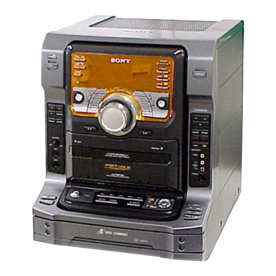
HCD-ZX6/ZX8
(Photo: HCD-ZX8)
Model Name Using Similar Mechanism
CD
CD Mechanism Type
Section
Base Unit Name
Optical Pick-up Name
TAPE
Model Name Using Similar Machanism
Section
Tape Mechanism Type
SPECIFICATIONS
Other models:
The following measured at AC 120, 220, 240 V, 50/60 Hz
DIN power output (rated):
Continuous RMS power output (reference):
Inputs
PHONO IN (phono jack):
MIC (phone jack):
GAME INPUT AUDIO L/R (phono jacks):
GAME INPUT VIDEO (phono jack):
VIDEO/MD IN L/R (phono jacks):
COMPONENT Hi-Fi STEREO SYSTEM
E Model
NEW
CDM79B-F1BD81
BU-F1BD81A
KSM-215DCP/C2RP
HCD-GN880
CWM43RR35
220 + 220 watts
(4 ohms at 1 kHz, DIN)
280 + 280 watts
(4 ohms at 1 kHz, 10% THD)
sensitivity 3 mV,
impedance 47 kOhms
sensitivity 1 mV,
impedance 10 kOhms
sensitivity 250 mV,
impedance 47 kOhms
1 Vp-p, 75ohms
sensitivity 250 mV/450 mV,
impedance 47 kOhms
– Continued on next page –
1
Advertisement
Table of Contents

Related Manuals for Sony HCD-ZX6


Summary of Contents for Sony HCD-ZX6
- Page 1 HCD-ZX6/ZX8 SERVICE MANUAL E Model Ver 1.1 2004. 09 • HCD-ZX6/ZX8 are the tuner, deck, CD and amplifier section in FST-ZX6/ZX8. (Photo: HCD-ZX8) Model Name Using Similar Mechanism CD Mechanism Type CDM79B-F1BD81 Section Base Unit Name BU-F1BD81A Optical Pick-up Name...
- Page 2 COMPONENTS IDENTIFIED BY MARK 0 OR DOTTED LINE WITH MARK 0 ON THE SCHEMATIC DIAGRAMS AND IN THE PARTS LIST ARE CRITICAL TO SAFE OPERATION. REPLACE THESE COMPONENTS WITH SONY PARTS WHOSE PART NUMBERS APPEAR AS SHOWN IN THIS MANUAL OR IN SUPPLEMENTS PUBLISHED BY SONY.
- Page 3 HCD-ZX6/ZX8 Notes on Chip Component Replacement NOTES ON LASER DIODE EMISSION CHECK • Never reuse a disconnected chip component. The laser beam on this model is concentrated so as to be focused on • Notice that the minus side of a tantalum capacitor may be the disc reflective surface by the objective lens in the optical pick- damaged by heat.
- Page 4 HCD-ZX6/ZX8 Ver 1.1 MODEL IDENTIFICATION PLAYABLE DISC You can playback the following discs on this system. The other – BACK PANEL – discs cannot be played back. List of playable discs Format of Disc logo Contents discs Part No. Audio CDs...
-
Page 5: Table Of Contents
HCD-ZX6/ZX8 TABLE OF CONTENTS 1. SERVICE NOTE 7-5. Schematic Diagram –BD Section– ........31 7-6. Printed Wiring Boards –Loading Section– ....... 32 1-1. Service Position of CD BU Block ........6 7-7. Schematic Diagram –Loading Section– ......33 1-2. Service Position of TC Mechanism, Panel Board ....7 7-8. -
Page 6: Service Note
HCD-ZX6/ZX8 SECTION 1 SERVICE NOTE 1-1. SERVICE POSITION OF CD BU BLOCK chassis CD block... -
Page 7: Service Position Of Tc Mechanism, Panel Board
HCD-ZX6/ZX8 1-2. SERVICE POSITION OF TC MECHANISM, PANEL BOARD gear (shaft) 3 loading panel 1 Turn the gear (shaft) in the direction of the arrow. PANEL board tape mechanism block... -
Page 8: Service Position Of Power Board
HCD-ZX6/ZX8 1-3. SERVICE POSITION OF POWER BOARD front panel assy CD mechanism block POWER board 1-4. SERVICE POSITION OF CD CHANGER CD mechanism block... -
Page 9: General
HCD-ZX6/ZX8 SECTION 2 GENERAL This section is extracted from instruction manual. - Page 10 HCD-ZX6/ZX8...
- Page 11 HCD-ZX6/ZX8...
-
Page 12: Disassembly
HCD-ZX6/ZX8 SECTION 3 DISASSEMBLY Note : Disassemble the unit in the order as shown below. 3-1. CASE 3-13. OPTICAL PICK-UP (Page 13) (Page 19) 3-2. LOADING PANEL 3-14. BD81A BOARD (Page 13) (Page 20) 3-3. FRONT PANEL SECTION (Page 14) 3-4. - Page 13 HCD-ZX6/ZX8 Note : Follow the disassembly procedure in the numerical order given. 3-1. CASE three claws 1 three screws BVTP3 x 8 3 case (top) three claws 7 case 6 three screws 4 four screws (case 3 TP2) BVTP3 x 8...
- Page 14 HCD-ZX6/ZX8 3-3. FRONT PANEL SECTION 0 screw BVTP3 x 8 2 CN104 (13P) 4 CN920 (3P) 3 CN507 (21P) 5 connector (3P) qf front panel section MAIN board dust sheet two hooks 1 two holes 9 CN801 (4P) 8 CN803 (3P)
- Page 15 HCD-ZX6/ZX8 3-5. GAME-IN/HP BOARD, MIC BOARD 8 four screws BVTP2.6 x 8 6 two screws qa two clips BVTP2.6 x 8 7 GAME-IN/HP board qd MIC board qs screw BVTP2.6 x 8 0 knob (MIC) 3 four screws BVTP2.6 x 8...
- Page 16 HCD-ZX6/ZX8 3-7. CD MECHANISM SECTION 2 CN501 (27P) 5 three screws BVTP3 x 8 7 chassis section 1 CN509 (11P) 4 two screws BVTP3 x 8 3 two screws BVTP3 x 8 9 two screws BVTP3 x 8 8 two screws...
-
Page 17: Main Board
HCD-ZX6/ZX8 3-8. MAIN BOARD 1 CN502 (4P) 6 MAIN board CN601 4 two screws BVTP3 x 8 CN602 3 CN509 (11P) 2 CN501 (27P) 3-9. TABLE ASSY 1 floating screw (+PTPWH M2.6) 2 tray qs table assy 7 screw 6 CN002 (6P) BTP2.6 x 8... -
Page 18: Board
HCD-ZX6/ZX8 3-10. SE-130 BOARD 4 two screws 5 CN101 (6P) 6 SE-130 board BTP2.6 x 8 1 CN102 (2P) 3 claw 2 claw 3-11. TD BELT 1 two screws BTP2.6 x 8 5 TD unit assy 4 TD belt 3 TD motor assy... -
Page 19: Dc Motor (M901)
HCD-ZX6/ZX8 3-12. DC MOTOR (M901) 6 DC motor (M901) 5 CN004 (2P) 3 belt (loading) 2 gear (loading A) 4 two screws 1 screw P2.6 x 4 (+ PTPWH M2.6 ) 3-13. OPTICAL PICK-UP holder (BU) assy 2 chassis plate... -
Page 20: Bd81A Board
HCD-ZX6/ZX8 3-14. BD81A BOARD 1 CN101 (16P) 5 BD81A board 3 gap tube 2 screw BVTP2.6 x 8 Remove soldering from the four points. -
Page 21: Test Mode
HCD-ZX6/ZX8 SECTION 4 TEST MODE [GC TEST MODE] 3. When b button or B button is pressed, GEQ is set to flat and • This mode is used to check the fluorescent indicator tube, LED, a message “GEQ FLAT” appears on the fluorescent indicator model, destination, software version, volume, key, jog and VACS tube. - Page 22 HCD-ZX6/ZX8 [TUNER STEP CHANGE] Aging mode sequence: • The step interval of AM channels can be toggled between 9 kHz and 10 kHz. START Procedure: (from Disc 1) 1. Press ?/1 button to turn the set ON. 2. Press [TUNER BAND] button to select the “AM”.
- Page 23 HCD-ZX6/ZX8 • Display when an error occurred (CD Error Code Mode) • Display of no disc errors Procedure: D*$$%%&&##00 1. Press x (TAPE B) button, [TUNER ENTER] button and [DISC SKIP] button simultaneously to enter the error code display D*: The number of no disc error (“00” is latest one) mode.
- Page 24 HCD-ZX6/ZX8 [CD SHIP MODE (WITHOUT MEMORY CLEAR)] • This mode moves the optical pick-up to the position durable to vibration. Use this mode when returning the set to the customer after repair. Procedure: 1. Press ?/1 button to turn the set ON.
-
Page 25: Mechanical Adjustments
HCD-ZX6/ZX8 SECTION 5 SECTION 6 MECHANICAL ADJUSTMENTS ELECTRICAL ADJUSTMENTS Precaution DECK SECTION 0 dB=0.775 V 1. Clean the following parts with a denatured alcohol-moistened swab: Precaution record/playback heads pinch rollers 1. Demagnetize the record/playback head with a head erase head rubber belts demagnetizer. - Page 26 HCD-ZX6/ZX8 Record/Playback Head Azimuth Adjustment Adjustment Location: Playback Head (Deck A). Record/Playback/Erase Head (Deck B). DECK A DECK B Note: Perform this adjustments for both decks Procedure: 1. Mode: Playback (FWD) test tape MAIN board P-4-A100 VIDEO/MD OUT jack (J701) (10 kHz, –...
- Page 27 HCD-ZX6/ZX8 Note: Clear RF signal waveform means that the shape “◊” can be CD SECTION clearly distinguished at the center of the waveform. Note: VOLT/DIV : 200mV 1. CD Block is basically designed to operate without adjustment. TIME/DIV : 500ns Therefore, check each item in order given.
-
Page 28: Diagrams
HCD-ZX6/ZX8 SECTION 7 DIAGRAMS 7-1. CIRCUIT BOARDS LOCATION VOL board VOLTAGE SELECTOR board PANEL board POWER SWITCH board POWER SWITCHING TC-A board FUNCTION SW board MIC board TC-B board CD-L board GAME-IN/HP board JOG board CD-R board CURSOR board TRANS board... -
Page 29: Note For Printed Wiring Boards And Schematic Diagrams
HCD-ZX6/ZX8 Ver 1.1 7-2. NOTE FOR PRINTED WIRING BOARDS AND SCHEMATIC DIAGRAMS 7-3. WAVEFORMS Note on Printed Wiring Board: Note on Schematic Diagram: — MAIN Board — — PANEL Board — • X : parts extracted from the component side. -
Page 30: Printed Wiring Board –Bd Section
HCD-ZX6/ZX8 7-4. PRINTED WIRING BOARD — BD SECTION — • Refer to page 28 for Circuit Boards Location. : Uses unleaded solder. M101 IC303 C305 C303 S101 R313 R419 C257 C315 R403 C316 C306 R352 M102 C313 R302 IC251 R301... -
Page 31: Schematic Diagram -Bd Section
HCD-ZX6/ZX8 • Refer to page 56 for IC Block Diagrams. 7-5. SCHEMATIC DIAGRAM — BD SECTION — • Refer to page 57 for IC Pin Description of IC101. CN101 R307 TP423 C125 C142 TP304 TP10 C307 C134 IC B/D TP11... -
Page 32: Printed Wiring Boards -Loading Section
HCD-ZX6/ZX8 7-6. PRINTED WIRING BOARDS — LOADING SECTION — • Refer to page 28 for Circuit Boards Location. : Uses unleaded solder. M902 TURN TABLE MOTOR SE-130 BOARD (13) MAIN BOARD CN509 (Page 38) MD-94 BOARD RE901 ROTARY ENCODER M901... -
Page 33: Schematic Diagram -Loading Section
HCD-ZX6/ZX8 7-7. SCHEMATIC DIAGRAM — LOADING SECTION — CN001 CN003 RE901 MAIN BOARD CN004 (3/4) CN509 M901 (Page 36) CN002 S001 CN102 CN101 M902 PH101 PH102 HCD-ZX6/ZX8... -
Page 34: Schematic Diagram –Main Section (1/4)
HCD-ZX6/ZX8 • Refer to page 29 for Waveforms. 7-8. SCHEMATIC DIAGRAM — MAIN SECTION (1/4) — • Refer to page 60 for IC Pin Description of IC401. Q196 R194 C187 R190 R191 D194 Q195 CN104 Q193 R189 R454 R176 R177... -
Page 35: Schematic Diagram -Main Section (1/4)
HCD-ZX6/ZX8 7-9. SCHEMATIC DIAGRAM — MAIN SECTION (2/4) — L104 R137 R299 HRPE901 R283 Q116 C156 C154 Q110 Q114 R282 Q115 C157 R124 TP101 C125 R129 R123 R199 Q103 R136 L103 Q112 Q104 TP103 R119 R121 L102 R158 C126 R122... -
Page 36: Schematic Diagram –Main Section (3/4)
HCD-ZX6/ZX8 Ver 1.1 7-10. SCHEMATIC DIAGRAM — MAIN SECTION (3/4) — • Refer to page 56 for IC Block Diagrams. (Page 34) CN501 C320 C322 R584 C401 C543 Q539 R433 Q402 MX MODEL Q540 E2,E51 MODEL R578 FB306 R579 FB305... -
Page 37: Schematic Diagram -Main Section (2/4)
HCD-ZX6/ZX8 7-11. SCHEMATIC DIAGRAM — MAIN SECTION (4/4) — (Page 35) Q203 R225 CN502 Q523 R558 R228 R559 R226 R227 R557 R554 (Page 53) Q204 R555 R229 R556 R561 R234 R231 Q524 R560 R232 (Page 36) NO512 (Page 51) TP520... -
Page 38: Printed Wiring Board –Main Section
HCD-ZX6/ZX8 Ver 1.1 7-12. PRINTED WIRING BOARD — MAIN SECTION — • Refer to page 28 for Circuit Boards Location. : Uses unleaded solder. (Page 54) VOLTAGE SELECTOR (Page 32) (Page 30) (Page 42) BOARD MD-94 BOARD CN001 BD81A BOARD CN201... -
Page 39: Printed Wiring Boards –Power Section
HCD-ZX6/ZX8 7-13. PRINTED WIRING BOARDS — POWER SECTION — • Refer to page 28 for Circuit Boards Location. : Uses unleaded solder. • Semiconductor Location Ref. No. Location SURROUND BOARD D609 TRANS NO701 D611 BOARD CN1113 (Page 52) D612 (Page 54) -
Page 40: Schematic Diagram -Power Section (1/2)
HCD-ZX6/ZX8 7-14. SCHEMATIC DIAGRAM — POWER SECTION (1/2) — R693 C637 R637 Q634 IC600 R640 R642 NO609 C634 R634 Q640 R635 Q635 C635 R638 R639 (Page 51) R643 R641 Q641 R618 C636 R636 C600 R600 C604 R619 C616 R603 R612... -
Page 41: Schematic Diagram -Power Section (2/2)
HCD-ZX6/ZX8 7-15. SCHEMATIC DIAGRAM — POWER SECTION (2/2) — JW682 RY646 JW680 JW720 TM609 JW699 R654 R655 R646 D654 D655 D646 R644 JW691 Q644 Q647 Q648 D661 R661 JW688 JW726 (Page 40) R647 C649 EP608 JR647 D660 R660 JW686 C648... -
Page 42: Printed Wiring Board -Panel Section
HCD-ZX6/ZX8 7-16. PRINTED WIRING BOARD — PANEL SECTION — • Refer to page 28 for Circuit Boards Location. : Uses unleaded solder. R941 D905 C944 C922 FL901 D906 S903 S928 Q908 SLEEP DISPLAY R942 D903 R990 C942 TUNER/BAND D901 C941... -
Page 43: Schematic Diagram -Panel Section
HCD-ZX6/ZX8 • Refer to page 29 for Waveform. 7-17. SCHEMATIC DIAGRAM — PANEL SECTION — • Refer to page 63 for IC Pin Description of IC901. Q902 NO910 FL901 (Page 51) C944 R941 R942 C922 R938 R939 C923 R1350 R948... -
Page 44: Printed Wiring Boards -Volume Section
HCD-ZX6/ZX8 7-18. PRINTED WIRING BOARDS — VOLUME SECTION — • Refer to page 28 for Circuit Boards Location. : Uses unleaded solder. D907-917 (ILLUMINATION) R968 S913 ROCK R963 S918 R970 S909 S904 R967 MENU SALSA SURROUND D912 JW909 S914 D911... -
Page 45: Printed Wiring Board -Mic Section
HCD-ZX6/ZX8 7-19. PRINTED WIRING BOARD — MIC SECTION — • Refer to page 28 for Circuit Boards Location. : Uses unleaded solder. MAIN BOARD NO511 (Page 38) 1-861-391- (13) HCD-ZX6/ZX8... -
Page 46: Schematic Diagram -Volume, Mic Section
HCD-ZX6/ZX8 7-20. SCHEMATIC DIAGRAM — VOLUME, MIC SECTION — R968 R969 S904 S913 C968 S975 R967 R970 C967 S914 S905 C971 R966 R971 S906 S915 R965 R972 EPT927 S907 S916 R964 R973 S917 S908 D908 D910 D912 D914 D916 R963... -
Page 47: Schematic Diagram -Switch Section
HCD-ZX6/ZX8 7-21. SCHEMATIC DIAGRAM — SWITCH SECTION — CN916 (Page 43) D921 D922 D923 D924 R847 R849 JR907 R857 R859 JR908 D926 Q909 Q910 R850 R860 R878 R879 R881 NO925 CN905 S930 R832 R872 NO919 NO901 R873 R874 R875 R876... -
Page 48: Printed Wiring Boards -Switch Section (1/2)
HCD-ZX6/ZX8 7-22. PRINTED WIRING BOARDS — SWITCH SECTION (1/2) — • Refer to page 28 for Circuit Boards Location. : Uses unleaded solder. PANEL BOARD CN908 (Page 42) (13) 1-861-392- Q907 R842 CLP804 NO900 R833 S938 R834 D919 D918 JR903... -
Page 49: Printed Wiring Boards -Switch Section (2/2)
HCD-ZX6/ZX8 7-23. PRINTED WIRING BOARDS — SWITCH SECTION (2/2) — • Refer to page 28 for Circuit Boards Location. : Uses unleaded solder. NO919 D924 S951 JW935 D923 S950 JR908 R869 R870 CN916 S949 S948 S930 FUNCTION R868 S953 S952... -
Page 50: Printed Wiring Boards -Jack Section
HCD-ZX6/ZX8 7-24. PRINTED WIRING BOARDS — JACK SECTION — • Refer to page 28 for Circuit Boards Location. : Uses unleaded solder. JW810 VIDEO MAIN BOARD NO512 C842 (Page 38) CN802 (CHASSIS) EPT803 J850 GAME R830 R828 INPUT JW811 MAIN... -
Page 51: Schematic Diagram -Jack Section
HCD-ZX6/ZX8 7-25. SCHEMATIC DIAGRAM — JACK SECTION — NO912 R1341 D920 (Page 43) R1342 R1338 S929 Q900 EPT803 C842 CN802 J850 R830 (Page 37) CN801 JW811 R828 R827 R829 (Page 35) C840 C841 EPT804 R826 CN803 J851 (Page 40) HCD-ZX6/ZX8... -
Page 52: Printed Wiring Board -Surround Section
HCD-ZX6/ZX8 7-26. PRINTED WIRING BOARD — SURROUND SECTION (HCD-ZX8 ONLY) — • Refer to page 28 for Circuit Boards Location. : Uses unleaded solder. • Semiconductor Location Ref. No. Location D720 D-11 D730 G-10 IC701 C753 C703 D760 D790 D791... -
Page 53: Schematic Diagram -Surround Section
HCD-ZX6/ZX8 7-27. SCHEMATIC DIAGRAM — SURROUND SECTION (HCD-ZX8 ONLY) — IC701 NO702 D791 R730 RY760 R700 C700 C703 (Page 37) R710 Q722 R731 C796 R794 R764 C730 D761 NO701 R702 R732 R795 Q730 C731 C702 C721 R797 C795 R793 C701... -
Page 54: Printed Wiring Boards -Transformer Section
HCD-ZX6/ZX8 Ver 1.1 7-28. PRINTED WIRING BOARDS — TRANSFORMER SECTION — • Refer to page 28 for Circuit Boards Location. : Uses unleaded solder. POWER SWITCH F1171 POWER F1151 BOARD NO607 (Page 39) F1161 F1141 T1100 POWER TRANSFORMER NEUTRAL (CHASSIS) -
Page 55: Schematic Diagram -Transformer Section
HCD-ZX6/ZX8 Ver 1.1 7-29. SCHEMATIC DIAGRAM — TRANSFORMER SECTION — F1141 FH1141 FH1142 E2,E51 MODEL EP1003 F1151 FH1151 FH1152 S1000 T1100 CN1112 F1161 FH1161 FH1162 JW1111 JW1121 F1171 FH1171 FH1172 JW1131 (Page 41) JW1004 NO1111 CN1004 C1004 F1181 FH1181 FH1182... -
Page 56: Ic Block Diagrams
HCD-ZX6/ZX8 7-30. IC BLOCK DIAGRAMS IC301 TC94A34FG-002 (BD81A Board) IC251 BA5947FM (BD81A Board) CH4OUTR CH1PUTF CH1OUTR CH4OUTF LRCKIA CH3OUTF CH2OUTF PIN26 6.5k CH2OUTR CH3OUTR BCKIA Vref POWVCC POWVCC (ch3, 4) (ch1, 2) 50k 50k 50k 50k SDI0 MUTE CNF4 50k 50k... -
Page 57: Ic Pin Descriptions
HCD-ZX6/ZX8 7-31. IC PIN DESCRIPTIONS • IC101 CXD3059AR (RF AMP) (BD81A BOARD) Pin No. Pin Name Pin Description MIRR Mirror signal input/output Not used in this set. (Open) DFCT Defect signal input/output Not used in this set. (Open) Focus OK signal input/output Not used in this set. (Open) —... - Page 58 HCD-ZX6/ZX8 Pin No. Pin Name Pin Description FILO Master PLL (slave=digital PLL) filter signal output FILI Master PLL filter signal input Master PLL charge pump signal output AVDD5 — Analog power supply pin (+3.3 V) DDVROUT DC/DC converter signal output...
- Page 59 HCD-ZX6/ZX8 Pin No. Pin Name Pin Description DATA Serial data signal input — Internal digital ground pin XLAT Latch signal input The serial data is latched at the falling edge CLOCK Serial data transfer clock signal input — Internal digital power supply pin (+3.3 V)
- Page 60 HCD-ZX6/ZX8 • IC401 M3062CMEN-A04FPUO (MASTER CONTROL) (MAIN BOARD (1/4)) Pin No. Pin Name Pin Description MP3 ACK Acknowledgement signal input from MP3 decoder IC “L”: acknowledged MP3 LP Latch signal output to MP3 decoder IC “L”: enable MP3 CS Chip select signal output MP3 decoder IC “L”: enable...
- Page 61 HCD-ZX6/ZX8 Pin No. Pin Name Pin Description OC SW1 Disc tray status detection signal input from CDM CHK SW Disc tray status detection signal input from CDM OC SW2 Disc tray status detection signal input from CDM TBL NEG CDM turning motor control signal output...
- Page 62 HCD-ZX6/ZX8 Pin No. Pin Name Pin Description A SHUT Shut off detection signal input from deck A side reel pulse detection (A/D input) B SHUT Shut off detection signal input from deck A side reel pulse detection (A/D input) B HALF Deck B cassette detection signal input “L”: cassette detected...
- Page 63 HCD-ZX6/ZX8 • IC901 MB90M407PF-G-141-BNDE1 (SYSTEM CONTROL) (PANEL BOARD) Pin No. Pin Name Pin Description 1 to 4 G4 to G1 Grid drive signal output to the fluorescent indicatore tube 5 to 10 SEG-1 to SEG-6 Segment drive signal output to the fluorescent indicatore tube VSS-IO —...
- Page 64 HCD-ZX6/ZX8 Pin No. Pin Name Pin Description JOG A Jog dial pulse signal input from X-ROUND JOG rotary encoder (B phase input) JOG B Jog dial pulse signal input from X-ROUND JOG rotary encoder (A phase input) RESET System reset signal input from the master control IC “L”: reset...
-
Page 65: Exploded Views
HCD-ZX6/ZX8 Ver 1.1 SECTION 8 EXPLODED VIEWS NOTE: • The mechanical parts with no reference • Accessories are given in the last of this The components identified by mark 0 or dotted line with mark number in the exploded views are not supplied. -
Page 66: Front Panel Section (2)
HCD-ZX6/ZX8 Ver 1.1 8-2. FRONT PANEL SECTION (1) not supplied (POWER SWITCH board) not supplied (CURSOR board) not supplied FL901 (TC-A board) not supplied not supplied (FUNCTION SW board) not supplied supplied with S975 Ref. No. Part No. Description Remark Ref. - Page 67 HCD-ZX6/ZX8 Ver 1.1 8-3. FRONT PANEL SECTION (2) not supplied not supplied supplied with jack not supplied not supplied supplied (MIC board) with jack not supplied not supplied not supplied not supplied (CD-L board) not supplied not supplied (CD-R board) not supplied Ref.
-
Page 68: Chassis Section
HCD-ZX6/ZX8 Ver 1.1 8-4. CHASSIS SECTION not supplied not supplied (SENSOR board) T1100 F1181 F1151 not supplied FC901 F1171 F1161 F1141 not supplied not supplied not supplied CDM79B-F1BD81 not supplied The components identified by mark 0 or dotted line with mark 0 are critical for safety. -
Page 69: Cd Mechanism Section (1)
HCD-ZX6/ZX8 8-5. CD MECHANISM SECTION (1) supplied supplied not supplied not supplied not supplied CD mechanism deck section-2 (CDM79B-F1BD81) Ref. No. Part No. Description Remark Ref. No. Part No. Description Remark 3-074-737-01 PLATE (GUIDE) 4-218-252-52 SCREW (+PTPWH M2.6), FLOATING A-6060-642-A SE-130 BOARD, COMPLETE... -
Page 70: Cd Mechanism Section (2)
HCD-ZX6/ZX8 8-6. CD MECHANISM SECTION (2) RE901 S101 M901 not supplied supplied supplied not supplied not supplied (MD-94 board) The components identified by mark 0 or dotted line with mark 0 are critical for safety. Replace only with part number specified. -
Page 71: Electrical Parts List
HCD-ZX6/ZX8 Ver 1.1 SECTION 9 BD81A ELECTRICAL PARTS LIST NOTE: • Due to standardization, replacements in • Items marked “*” are not stocked since The components identified by mark 0 or dotted line with mark the parts list may be different from the they are seldom required for routine service. - Page 72 HCD-ZX6/ZX8 BD81A CD-L CD-R Ref. No. Part No. Description Remark Ref. No. Part No. Description Remark < TRANSISTOR > R410 1-216-809-11 METAL CHIP 1/10W R411 1-216-809-11 METAL CHIP 1/10W 6-550-363-01 TRANSISTOR 2SB1690KT146 R412 1-216-809-11 METAL CHIP 1/10W R419 1-216-809-11 METAL CHIP 1/10W <...
- Page 73 HCD-ZX6/ZX8 Ver 1.1 CURSOR FUNCTION SW GANE-IN/HP Ref. No. Part No. Description Remark Ref. No. Part No. Description Remark CURSOR BOARD A-1053-210-A JOG BOARD, COMPLETE (ZX8:MX) A-4751-078-A JOG BOARD, COMPLETE (ZX8:E2,E51) ************** A-4751-092-A JOG BOARD, COMPLETE (ZX6) < RESISTOR >...
- Page 74 HCD-ZX6/ZX8 Ver 1.1 MAIN Ref. No. Part No. Description Remark Ref. No. Part No. Description Remark A-1058-331-A MAIN BOARD, COMPLETE (ZX8:MX) C159 1-126-964-11 ELECT 10uF A-4751-049-A MAIN BOARD, COMPLETE (ZX8:E2,E51) C160 1-126-960-11 ELECT A-4751-086-A MAIN BOARD, COMPLETE (ZX6) C161 1-126-964-11 ELECT...
- Page 75 HCD-ZX6/ZX8 Ver 1.1 MAIN Ref. No. Part No. Description Remark Ref. No. Part No. Description Remark C241 1-126-964-11 ELECT 10uF C514 1-162-953-11 CERAMIC CHIP 100PF (ZX8) C515 1-126-964-11 ELECT 10uF C242 1-162-960-11 CERAMIC CHIP 220PF C516 1-126-964-11 ELECT 10uF (ZX8)
- Page 76 HCD-ZX6/ZX8 Ver 1.1 MAIN Ref. No. Part No. Description Remark Ref. No. Part No. Description Remark D408 6-500-522-21 DIODE 10EDB40-TB3 JR119 1-216-864-11 SHORT CHIP D501 8-719-500-56 DIODE D3SBA20 JR121 1-216-864-11 SHORT CHIP D503 6-500-522-21 DIODE 10EDB40-TB3 JR131 1-216-864-11 SHORT CHIP...
- Page 77 HCD-ZX6/ZX8 Ver 1.1 MAIN Ref. No. Part No. Description Remark Ref. No. Part No. Description Remark Q109 8-729-027-43 TRANSISTOR DTC114EKA-T146 R107 1-216-821-11 METAL CHIP 1/10W Q110 8-729-216-22 TRANSISTOR 2SA1162-G R108 1-216-838-11 METAL CHIP 1/10W Q111 8-729-802-80 TRANSISTOR 2SC3661 R109 1-216-825-11 METAL CHIP 2.2K...
- Page 78 HCD-ZX6/ZX8 Ver 1.1 MAIN Ref. No. Part No. Description Remark Ref. No. Part No. Description Remark R173 1-216-825-11 METAL CHIP 2.2K 1/10W R245 1-216-841-11 METAL CHIP 1/10W R174 1-216-825-11 METAL CHIP 2.2K 1/10W (ZX8) R175 1-216-819-11 METAL CHIP 1/10W R247...
- Page 79 HCD-ZX6/ZX8 Ver 1.1 MAIN Ref. No. Part No. Description Remark Ref. No. Part No. Description Remark R401 1-216-837-11 METAL CHIP 1/10W R487 1-216-833-11 METAL CHIP 1/10W R402 1-216-809-11 METAL CHIP 1/10W R492 1-216-829-11 METAL CHIP 4.7K 1/10W R403 1-216-809-11 METAL CHIP...
- Page 80 HCD-ZX6/ZX8 Ver 1.1 MAIN MD-94 PANEL Ref. No. Part No. Description Remark Ref. No. Part No. Description Remark R585 1-216-829-11 METAL CHIP 4.7K 1/10W < CONNECTOR > (ZX8) R585 1-216-837-11 METAL CHIP 1/10W * CN920 1-564-705-11 PIN, CONNECTOR (SMALL TYPE) 3P...
- Page 81 HCD-ZX6/ZX8 Ver 1.1 PANEL Ref. No. Part No. Description Remark Ref. No. Part No. Description Remark C926 1-162-927-11 CERAMIC CHIP 100PF < VACUUM FLUORESCENT DISPLAY > C927 1-162-927-11 CERAMIC CHIP 100PF C928 1-162-927-11 CERAMIC CHIP 100PF FL901 1-518-978-11 VACUUM FLUORESCENT DISPLAY...
- Page 82 HCD-ZX6/ZX8 Ver 1.1 PANEL POWER Ref. No. Part No. Description Remark Ref. No. Part No. Description Remark R950 1-216-821-11 METAL CHIP 1/10W C605 1-162-970-11 CERAMIC CHIP 0.01uF R951 1-216-830-11 METAL CHIP 5.6K 1/10W C608 1-126-965-11 ELECT 22uF R952 1-216-821-11 METAL CHIP...
- Page 83 HCD-ZX6/ZX8 Ver 1.1 POWER Ref. No. Part No. Description Remark Ref. No. Part No. Description Remark D646 8-719-404-50 DIODE MA111-TX 0 R612 1-245-605-51 FUSIBLE 1/4W F 0 R613 D654 8-719-404-50 DIODE MA111-TX 1-215-869-11 METAL OXIDE D655 8-719-404-50 DIODE MA111-TX (ZX8)
- Page 84 HCD-ZX6/ZX8 Ver 1.1 POWER POWER SWITCH SE-130 SENSOR SURROUND Ref. No. Part No. Description Remark Ref. No. Part No. Description Remark R652 1-218-484-11 METAL CHIP 1/10W < TRANSISTOR > (ZX6) R653 1-216-841-11 METAL CHIP 1/10W Q900 8-729-027-43 TRANSISTOR DTC114EKA-T146 R654...
- Page 85 HCD-ZX6/ZX8 Ver 1.1 SURROUND Ref. No. Part No. Description Remark Ref. No. Part No. Description Remark C753 1-162-927-11 CERAMIC CHIP 100PF R725 1-216-843-11 METAL CHIP 1/10W (ZX8) (ZX8) C780 1-136-495-11 FILM 0.068uF R726 1-216-843-11 METAL CHIP 1/10W (ZX8) (ZX8) C781 1-136-495-11 FILM 0.068uF...
- Page 86 HCD-ZX6/ZX8 Ver 1.1 SURROUND TC-A TC-B TRANS Ref. No. Part No. Description Remark Ref. No. Part No. Description Remark R798 1-216-845-11 METAL CHIP 100K 1/10W D924 8-719-060-27 LED SLR-325MCT31 (G) (ZX8) R799 1-216-845-11 METAL CHIP 100K 1/10W < JUMPER RESISTOR >...
- Page 87 HCD-ZX6/ZX8 Ver 1.1 VOLTAGE SELECTOR Ref. No. Part No. Description Remark Ref. No. Part No. Description Remark A-1052-687-A VOL BOARD, COMPLETE (ZX8:MX) R976 1-216-829-11 METAL CHIP 4.7K 1/10W A-4751-069-A VOL BOARD, COMPLETE (ZX8:E2,E51) R1300 1-216-821-11 METAL CHIP 1/10W A-4751-091-A VOL BOARD, COMPLETE (ZX6)
- Page 88 HCD-ZX6/ZX8 Ver 1.1 VOLTAGE SELECTOR Ref. No. Part No. Description Remark < DIODE > D1000 8-719-404-50 DIODE MA111-TX < JUMPER RESISTOR > JR1002 1-216-864-11 SHORT CHIP < COIL > L1001 1-410-666-31 INDUCTOR 18uH < TRANSISTOR > Q1000 8-729-901-81 TRANSISTOR 2SC2412K-T-146-R <...
- Page 89 HCD-ZX6/ZX8 E Model SERVICE MANUAL Ver 1.1 2004. 09 SUPPLEMENT-1 File this supplement with the service manual. Subject : Addition of Block Diagrams. 9-879-083-81...
- Page 90 HCD-ZX6/ZX8 TABLE OF CONTENTS 1. Block Diagram –CD Servo Section– ........3 2. Block Diagram –Tuner/Tape Deck Section– ......4 3. Block Diagram –Main Section– ..........5 4. Block Diagram –Display/Power Section– ....... 6...
-
Page 91: Block Diagram -Cd Servo Section
HCD-ZX6/ZX8 1. BLOCK DIAGRAM — CD SERVO SECTION — RF AMP,DIGITAL SIGNAL PROCESSOR OPTICAL PICK-UP IC101 BLOCK (KSM-215DCP) MAIN AOUT1 CD L SECTION (Page 5) AOUT2 R-CH DETECTOR DIGITAL OUT IC503 MUTE +1.7V Q551 +3.3V DIGITAL DOUT DOUT (OPTICAL) CD MUTE... -
Page 92: Block Diagram -Tuner/Tape Deck Section
HCD-ZX6/ZX8 2. BLOCK DIAGRAM — TUNER/TAPE DECK SECTION — HP901 DECK-A PB L(DECK A) MAIN PB L(DECK B) HEAD SECTION R-CH (Page 5) Q103 ST L TC RELAY A+9V CONTROL Q106,107 HRPE901 DECK-B MAIN REC/PB REC L(DECK B) SECTION HEAD... -
Page 93: Block Diagram -Main Section
HCD-ZX6/ZX8 3. BLOCK DIAGRAM — MAIN SECTION — HCD-ZX8 MIC AMP POWER AMP IC850 (1/2) SURROUND J801 MIC AMP IC501 POWER AMP IC850 (2/2) MIC1 IC701 TM609 RV801 SURROUND LEVEL R-CH MUTE OVERLOAD RY760 Q203 DETECT J802 SPEAKER Q722 OVERLOAD... -
Page 94: Block Diagram -Display/Power Section
HCD-ZX6/ZX8 4. BLOCK DIAGRAM — DISPLAY/POWER SECTION — FLUORESCENT INDICATOR TUBE DRIVER, KEY CONTROL BAND-PASS FILTER IC901 IC903 BPF1OUT POWER BPF1-F01 SWITCHING BPF2OUT EVER+4V BPF1-F02 BLOCK BPF3OUT MAIN SPEANA BPF2-F03 B.P.F. T1100 SECTION BPF4OUT POWER BPF3-F04 73 (Page 5) E2,E51 MODEL... - Page 95 HCD-ZX6/ZX8 MEMO...
- Page 96 HCD-ZX6/ZX8 REVISION HISTORY Clicking the version allows you to jump to the revised page. Also, clicking the version at the upper on the revised page allows you to jump to the next revised page. Ver. Date Description of Revision 2004. 07 2004.