Table of Contents
Advertisement
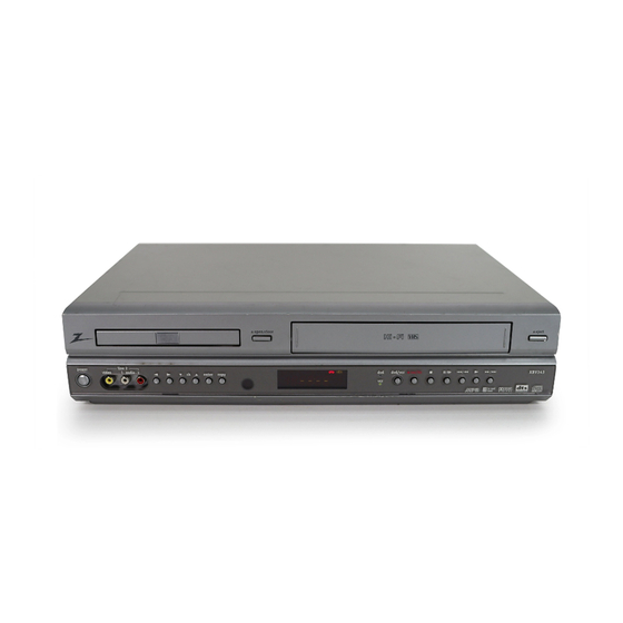
SERVICE MANUAL
Product Type: DVD+VCR
Chassis: D35 (DECK), DP5 (MD), DP-7C(MD)
Manual Series: XBV342
Manual Part #: 3829RGN001V
Model Line: C
Product Year: 2003
CONTENTS
....................................................
Summary
Cabinet & Main Chassis
....................................................
Electrical
Mechanism of VCR Part
Mechanism of DVD Part
....................................................
Parts List
Published September 2003
by Technical Publications
Zenith Electronics Corporation
201 James Record Road
Huntsville, Alabama 35824-1513
Copyright © 2003 by Zenith Electronics Corporation
1
.............................
2
3
.............................
4
.............................
5
6
Model Series:
ABV341
XBV342
XBV343
Advertisement
Chapters
Table of Contents
Troubleshooting

Related Manuals for Zenith ABV341 Series


Summary of Contents for Zenith ABV341 Series
- Page 1 Cabinet & Main Chassis ............ Electrical ......Mechanism of VCR Part ......Mechanism of DVD Part ............ Parts List Published September 2003 by Technical Publications Zenith Electronics Corporation 201 James Record Road Huntsville, Alabama 35824-1513 Copyright © 2003 by Zenith Electronics Corporation...
- Page 3 SECTION 1 SUMMARY CONTENTS PRODUCT SAFETY SERVICING GUIDELINES FOR VIDEO PRODUCTS ..... 1-2 SERVICING PRECAUTIONS ....................1-3 SPECIFICATIONS ........................1-4...
- Page 4 When servicing this product, under no circumstances should the original design be modified or altered without permission from Zenith Electronics Corporation. All components should be replaced only with types identical to those in the original circuit and their physical location, wiring and lead dress must conform to original layout upon completion of repairs.
-
Page 5: Servicing Precautions
SERVICING PRECAUTIONS CAUTION: Before servicing the DVD+VCR covered by this Electrostatically Sensitive (ES) Devices service data and its supplements and addends, read and fol- Some semiconductor (solid state) devices can be damaged low the SAFETY PRECAUTIONS. NOTE: if unforeseen cir- easily by static electricity. -
Page 6: Specifications
SPECIFICATIONS General Power requirements AC 120V ,60 Hz Power consumption Dimensions (approx.) 430 X 97.5 X 293 mm (16.9 x 3.9 x 11.5 inches)(w x h x d) Mass (approx.) 4.8 kg (10.58 lbs) Operating temperature 5 °C to 40 °C (41 °F to 104 °F) Operating humidity 5 % to 90 % Signal system... - Page 7 SECTION 2 CABINET & MAIN CHASSIS CONTENTS 1. EXPLODED VIEWS ........................2-2 1. Cabinet and Main Frame Section ...................2-2 2. Packing Accessory Section ....................2-3...
-
Page 8: Cabinet And Main Frame Section
EXPLODED VIEWS 1. Cabinet and Main Frame Section OPTIONAL PARTS... -
Page 9: Packing Accessory Section
2.Packing Accessory Section OPTIONAL PARTS 810 CABLE ASS'Y RF CABLE(COAXIAL) PLUG ASS'Y 1WAY BATTERY PLUG ASS'Y 2WAY REMOCON INSTRUCTION ASSEMBLY PACKING PACKING BOX CARTON... -
Page 10: Table Of Contents
SECTION 3 ELECTRICAL CONTENTS OVERALL WIRING DIAGRAM 2. DRIVE & RF CIRCUIT DIAGRAM ......3-72 ......3-2 3. MEMORY CIRCUIT DIAGRAM ......3-74 VCR PART 4. INTERFACE CIRCUIT DIAGRAM......3-76 5. µ-COM/Expander CIRCUIT DIAGRAM....3-78 ELECTRICAL ADJUSTMENT 6. Jack CIRCUIT DIAGRAM ........3-80 PROCEDURES ............3-3 • WAVEFORMS ............3-82 ELECTRICAL TROUBLESHOOTING •... -
Page 11: Overall Wiring Diagram
OVERALL WIRING DIAGRAM... -
Page 12: Vcr Part
VCR PART ELECTRICAL ADJUSTMENT PROCEDURES 1. Servo Adjustment 1) PG Adjustment • Test Equipment a) OSCILLOSCOPE b) NTSC MODEL : NTSC SP TEST TAPE • Adjustment And Specification MODE MEASUREMENT POINT ADJUSTMENT POINT SPECIFICATION V.Out PLAY R/C TRK JIG KEY 6.5 ±... -
Page 13: Electrical Troubleshooting Guide
ELECTRICAL TROUBLESHOOTING GUIDE 1. Power(SMPS) CIRCUIT (1) No 5.3VA (SYS/Hi-Fi/TUNER) (2) No 12VA (TO CAP, DRUM MOTOR) NO 5.3VA. NO 12VA. Replace the F101. Is the Vcc(13V) supplied Check or Replace Is the F101 normal? (Use the same Fuse) to (+) terminal in D115? the D110. - Page 14 (4) No 5V (TO DVD) (5) No 33V (TUNER) NO 5V. No 33V. Is 5.3VA put into Check the Power 5.3VA Line Check. Is Q162 Base “H”? the Q160 Emitter? Control. Is the Q162 Base Check the Power Check or Replace “H”? Control.
- Page 15 (8) No 8V(TO DVD) (9) No 3.3V(TO DVD) NO 8V. NO 3.3V. Check or Replace Check or Replace Is Vcc(13V) supplied to Is Vcc(4V) supplied (+) terminal in D114? to IC152 Pin1? the D110. the D111. Check or Replace Check the Power Is Vcc(12V) supplied Is the Q162 Base to IC151 Pin1?
-
Page 16: System/Key Circuit
2. SYSTEM/KEY CIRCUIT (1) AUTO STOP Auto Stop Does the SW30 waveform Check the Drum Motor appear at the IC501 signal. Pin18? Do T/UP Reel Pulses Do the T-UP Reel Pulses Does 5V appear at the appear at the point appear at the IC501 Pin80? RS501? between R556 and R536? -
Page 17: Servo Circuit
3. SERVO CIRCUIT (1) Unstable Video in PB MODE Unstable Video in PB Mode. Does the Noise level of the screen change periodically? Do the CTL pulses appear Is adjusting the height of at the IC501 Pin97? the CTL Head accurate? Does the CFG waveform Readjust the height of the appear at the IC501... - Page 18 2. SERVO CIRCUIT (3) When the Capstan Motor doesn’t run, When the Capstan Motor doesn’t run, Refer to “SMPS(CAPSTAN/12Volt) Does 12VA appear at the PMC01? Trouble Shooting”. Does 2.8V appear at the PMC01? Check the PMC01 and the Capstan Does the PWM signal appear at the Motor Ass’y.
-
Page 19: Osd Circuit
2. SERVO CIRCUIT (4) KEY doesn’t working KEY doesn’t working. Is 5V applied to the IC501 Refer to “SMPS 5.3VA Pin79? Trouble Shooting”. Does LED or FLD change Replace the defective when a function button is switches. pressed? 4. OSD CIRCUIT (1) No OSD display. -
Page 20: Y/C Circuit
5. Y/C CIRCUIT (1) No Video in EE Mode, No Video in EE Mode Does the Video signal Does the Video signal Check DVD Video Input appear at the IC301 appear at the IC302 (IC802, Pin29), Tuner Pins28, 30, 32? Pins1, 5? Video Input (TU701 Pin24), Line Video Input (JK801),... - Page 21 3. Y/C CIRCUIT (2) When the Y(Luminance) signal doesn’t appear on the screen in PB Mode, Is 5V applied to the IC301 Check the line of the REG Pins23, 44, 45, 52, 68, 77? 5V Line. (Power Circuit) Is the Y/C Bus siganl Refer to ‘SYSTEM Y/C applied to the IC301 BUS CHECK Trouble...
- Page 22 3. Y/C CIRCUIT (3) When the C(Color) signal doesn’t appear on the screen in PB Mode, Is 5V applied to the IC301 Check the line of the REG Pins23, 44, 45, 52, 68, 77? 5V Line. (Power Circuit) Does the Color signal Is normal the X301 appear at the IC301 (3.58MHZ) of oscillation...
- Page 23 3. Y/C CIRCUIT (4) When the Video signal doesn’t appear on the screen in REC Mode, REC mode Is EE mode normal? Check the EE mode Is brightness normal? Is color normal? Is the brightness signal sup- Does signal appear at Check X301 oscillation IC301 Pins41, 50? frequency.
-
Page 24: Hi-Fi Circuit
6. Hi-Fi CIRCUIT (1) No Sound(EE Mode) No Sound. Check the SIF.IN of IC801 Pins57. Check the TU701 SIF Pin13. Check the DVD Audio of IC801 Check the DVD MODULE. (PMD02 Pins9, 11). Pins12, 74. Check the AV1 Audio of IC801 Check the Rear Jack. - Page 25 3. Y/C CIRCUIT (2) Hi-Fi Playback PB mode No Sound. Check the Vcc of IC801 Check Power. (Pins3, 5, 15, 32, 36, 46, 54). Check the Hi-Fi Selection switch. Check IC501 Pin19 (IC801 Pin39) and the Tape quality. (A.H/SW) Is the RF Envelope at IC801 Pin23 over 3Vp-p? Check IC801 Pin37(Data), Check the parts of µ-COM...
- Page 26 (3) Hi-Fi REC Hi-Fi REC. It is impossible to record Hi-Fi Audio signal. Check Vcc of IC801. Check Power. (Pins3, 5, 15, 32, 36, 46, 54) Check ports of µ-CPM. Check IC801 Pin37(Data), Pin38(CLOCK). (IC501 Pins71, 72) Check Audio input signal of IC801 Do Audio signals appear at IC801 Pin6? Pin57(TU.A.), 7, 69(DVD.A.), 11, 73(AVI.A.), 9, 71(AV2.A.)
-
Page 27: Tuner/If Circuit
7. Tuner/IF CIRCUIT (1) No Picture on the TV screen No picture on the TV screen Does the Video signal at Is +33V applied to TU701 Check 33V line. the TU701 Pin16. Pin14? Is +5V applied to TU701 Check 5V line. Pin3? Does the Clock signal Check the lIC Clock Signal... - Page 28 (2) No Sound No Sound. Check the Vcc of TU701 Pins3, 14. Check 5.2V, 33V Line. Check the Tuner SiF signal at IC801 Check the Tuner SIF of TU701 Pin13. Pin57. 1. Check the Vcc(5.3VA, 9V) of IC801 Check the Audio of IC801 Pins78, 80. Pins3, 5, 36, 54.
-
Page 29: Block Diagrams
5V BLOCK R117) IC102 TO DVD (R157, Q160, R158, R159, D121, C155) IC103 (BK) (WH) HOT CIRCUIT PWR CTL FROM µ-COM BLOCK PWR CTL 'H' (Q162,R163,R164, R171,C161) NOTES : Symbol denotes AC ground. Symbol denotes DC chassis ground. ZENITH 3-20 3-21... -
Page 30: Tu/If Block Diagram
2. TU/IF BLOCK DIAGRAM 875 MOD A.IN MOD CTL 106 5.0V VCR 'H' REG. BLOCK 671 MOD V.IN IIC CLK REG. BLOCK IIC DATA 781 SIF OUT TU.V.OUT ZENITH 3-22 3-23... -
Page 31: Y/C Block Diagram
BPF2 3.58M VIDEO BPF1 MAIN C-LPF 4.21M CONV 3.58M BPF1 COMB 4.21M DETAIL CLAMP CONV COMB LINE2 MAIN SP REC CLAMP EMPHA CONV EMPHA SP PB 'B' SP PB 'A' V.OUT V.OUT DOUBLE FM-EQ MAIN DE-EM FM-EQ ZENITH 3-24 3-25... -
Page 32: Normal Audio Block Diagram
4. NORMAL AUDIO BLOCK DIAGRAM (EE Mode) (PB Mode) (REC Mode) ZENITH 3-26 3-27... -
Page 33: Hi-Fi Block Diagram
DVD A.IN 'L' A.OUT To JACK A.OUT 'R' IC801 DVD A.IN 'R' AV1 A.IN 'L' LA72670M AV1 A.IN 'R' MODULATOR AV2 A.IN 'L' A.OUT (To Tu) AV2 A.IN 'R' NORMAL AUDIO OUT(To AVCP) NORMAL AUDIO IN(From AVCP) ZENITH 3-28 3-29... -
Page 34: System Block Diagram
POWER FAIL SUP REEL R558 C582 IC504 CST IN RESET CST.SW/REC TAP Q503 5.3VA IC505 5.3VA C500 C517 R541 R531 CS501 R5C6 RC601 R544 Q501 L511 C552 R583 R529 R598 C595 C596 L512 C592 C503 C561 L501 ZENITH 3-30 3-31... -
Page 35: Circuit Diagrams
2. Voltages are DC-measured with a digital voltmeter MODIFIED OR ALTERED WITHOUT PERMISSION IMPLEMENTATION OF THE LATEST SAFETY AND during Play mode. FROM THE ZENITH ELECTRONICS CORPORATION. PERFORMANCE IMPROVEMENT CHANGES INTO ALL COMPONENTS SHOULD BE REPLACED ONLY THE SET IS NOT DELAYED UNTIL THE NEW SERVICE WITH TYPES IDENTICAL TO THOSE IN THE ORIGI- LITERATURE IS PRINTED. -
Page 36: Tu/If Circuit Diagram
2. TU/IF CIRCUIT DIAGRAM 3-34 3-35... -
Page 37: A/V Circuit Diagram
3. A/V CIRCUIT DIAGRAM IC301 Pins 53, 54, 55 are defective. IC301 doesn’t operate. IC301 is defective. PB COLOR Signal does not appear. IC301 Pin 57 is defective. PB COLOR Signal does not appear. IC301 Pin 59 is defective. Auto Tracking has failed. IC306, Q307 are defective. -
Page 38: Hi-Fi Circuit Diagram
4. Hi-Fi CIRCUIT DIAGRAM IC801 Pins37, 38 aredefective. All Audio is not appear. KTC3875 23 Pin is defective. Hi-Fi Audio is not appear. '02. 12. 04 R13734C 3-38 3-39... -
Page 39: Jack Circuit Diagram
5. JACK CIRCUIT DIAGRAM 3-40 3-41... -
Page 40: System Circuit Diagram
6. SYSTEM CIRCUIT DIAGRAM • Reset is defective. • Set dead. IC504 is defective. MTZ5.6B MTZ5.6B VCR LCD DVD LED IC501 M37762 µ-COM will not operate. X502 is defective. CLOCK SETTING will not operate. X501 is defective. C542 680P µ-COM is unstable. Q501, Q503 are defective. -
Page 41: Timer Circuit Diagram(Xbv343)
7. TIMER CIRCUIT DIAGRAM(XBV343) 3-44 3-45... -
Page 42: Timer Circuit Diagram(Xbv342)
8. TIMER CIRCUIT DIAGRAM(XBV342) 3-46 3-47... -
Page 43: Waveforms
• WAVEFORMS * IC301 Waveform * IC501 Waveform Stop : 10.0KS/s 280 Acqs Stop : 250KS/s 299 Acqs Stop : 10.0KS/s 18 Acqs Trigger Position: 12% Stop : 10.0KS/s 27 Acqs 1.00 V M 5.00ms 3.04 V 1.00 V M5.00ms 3.04 V 1.00 V M 200µs... -
Page 44: Circuit Voltage Chart
• CIRCUIT VOLTAGE CHART MODE MODE MODE MODE MODE MODE Base Emitter Collector Location PLAY PLAY PLAY PLAY PLAY PLAY PIN NO. PIN NO. PIN NO. PIN NO. PIN NO. PIN NO. I C 3 0 1 0.68 0.93 5.19 5.19 3.86 0.23... -
Page 45: Printed Circuit Diagrams
PRINTED CIRCUIT DIAGRAMS 1. MAIN P.C.BOARD LOCATION GUIDE 3-52 3-53... -
Page 46: Key 1(Left) P.c.board
2. KEY 1(LEFT) P.C.BOARD (XBV342) (XBV343) LOCATION GUIDE LOCATION GUIDE 3. KEY 2(RIGHT) P.C.BOARD (XBV342) LOCATION GUIDE (XBV343) LOCATION GUIDE 3-54 3-55... -
Page 47: Power P.c.board
4. POWER P.C.BOARD NOTES) Warning NOTES) Parts that are shaded are critical NOTES) With respect to risk of fire or NOTES) electricial shock. LOCATION GUIDE 3-56 3-57... -
Page 48: Dvd Part(Ns Model) Electrical Troubleshooting Guide
DVD PART(NS MODEL) ELECTRICAL TROUBLESHOOTING GUIDE 1. µ-COM Circuit A. No Power POWER ON Does Hello appear at FLD? Is PDV02 Does no DISC appear? connected normally? Reconnect it. Does Logo appear Check power. on the screen? (Refer to power) If power is normal Is PDV02 Pins8, 9,... - Page 49 B. Audio abnormal C. Video abnormal AUDIO ABNORMAL VIDEO ABNORMAL Check Audio jack. Check Video jack. YES (If OK) YES (If OK) Check MPEG_CLK Signal Refer to Video part. (IC501 Pin22) of MPEG part. YES (If OK) YES (If OK) Refer to Audio part.
- Page 50 E. Picture abnormal PICTURE ABNORMAL Check the disc. Refer to Servo part If OK Check MPEG_CLK Signal (IC501 Pin22) of MPEG part YES (If OK) Check DSP YES (If OK) Check MPEG YES (If OK) Replace Main B/D F. Disc Error DISC ERROR Check Disc YES (If OK)
-
Page 51: Mpeg Circuit
2. MPEG Circuit Power is on Does Logo appear Check power & clock. on the screen? Does the Check CD/DVD DSP output moving picture of the DVD Disc Is MPEG data signal normal? play on the screen signal. normally? Check MPEG Decoder input signal. -
Page 52: Rf/Servo Circuit
3. RF/Servo Circuit CHECK POINT(General) Does signal goes "High" to IC201 Pin186 when the power is on? Does signal pulse Check "2.µ-COM Part". input to IC201 Pins53, 54 when the power is on? Does Does Replace X201 or IC206 33.8688MHz clock input to 33.8688MHz clock input (33MHz clock defect) IC201 Pin138? - Page 53 No disc Power on. Check loading Part. Push Pick-up to inner track to Does tray open or close? the end by hand. Does DECK assembly is defective. PMD03 Pin10 change (Limit sw) high to low? Pressing the open/close key repeatedly, check the voltage of IC2M1 check µ-COM Part.
- Page 54 DISC IN OPEN/CLOSE Fig.3. FOCUS ERROR waveform Check Check IC2A1 Pins47,50,51,52 the focus error moving the FOCUS ON? lens up and down. in DVD Mode (IC2A1 Pin39) IC201 no output : Pick-up is defective. Does the TTL level change at IC201 Replace IC201.
- Page 55 CHECK A Fig.5. RF waveform Check RF Eye-Pattern. Check IC2A1 Pin3. No signal: Pick-up is defective RF : 1.5-1.6V(TP2A0) Does the sawtooth waveform emit Is the eye-pattern vivid? Does the 1.6V emit? Replace IC2A1. at IC2A1 Pin36? Replace IC201. Check IC201 Pin84. No signal at IC201 : IC201 is defective •...
-
Page 56: Block Diagrams
BLOCK DIAGRAMS 1. DVD OVERALL BLOCK DIAGRAM , PAL_SW , AUTO_SW , MIC_ON DAC_RST /FLASH_CS , /RD PWEO PSENB MIRR,TZC,PE,TE FE,DFECT_IN XLAT , E_STI , E_ENB , E_DR CPLD SPINDLE FOCUS,TRACKI NG,SLED LOADING ZENITH DECK M ECHANI SM 3-66... -
Page 57: Rf/Cd Dsp/Dvd Dsp/Dvd Servo Block Diagram
2. RF/CD DSP/DVD DSP/DVD SERVO BLOCK DIAGRAM ZENITH 3-67... -
Page 58: Audio Block Diagram
3. AUDIO BLOCK DIAGRAM ZENITH 3-68... -
Page 59: Memory Block Diagram
4. MEMORY BLOCK DIAGRAM AD[ 04 : 21 ] ZENITH 3-69... -
Page 60: Circuit Diagrams
CIRCUIT DIAGRAMS 1. DVD DSP CIRCUIT DIAGRAM TO/FROM MPEG DSP II '02. 12. 04 R17147A TRACKING LOOP SLED LOOP ZENITH WAVEFORM FOCUS LOOP SPINDLE LOOP 3-70 3-71... -
Page 61: Drive & Rf Circuit Diagram
2. DRIVE & RF CIRCUIT DIAGRAM TO/FROM MEMORY Q2A5, Q2A6 TO/FROM DSP TO/FROM DSP TO/FROM MEMORY TO/FROM MPEG TO/FROM MEMORY TO/FROM DSP TO/FROM DSP '02. 12. 04 R17145A ZENITH TRACKING LOOP SLED LOOP WAVEFORM FOCUS LOOP SPINDLE LOOP 3-72 3-73... -
Page 62: Memory Circuit Diagram
DRIVE & RF Digitron all not display system not working Tray not open/close Digitron all not display '02. 12. 04 R17148A system not working 6870R9241AA 6870R9241AB Tray not open/close ZENITH C324 0.1µ C307 0.1µ 1µ 3-74 3-75... -
Page 63: Interface Circuit Diagram
4. INTERFACE CIRCUIT DIAGRAM (TO/FROM VCR POWER) PDV01-PPD01 (TO/FROM VCR SYSTEM) PDV02-PMD01 TO/FROM MPEG TO/FROM JACK TO/FROM MPEG (TO/FROM VCR JACK) PDV03-PMD02 TO/FROM MEMORY '02. 12. 04 R17150A ZENITH 3-76 3-77... -
Page 64: Μ-Com/Expander Circuit Diagram
5. µ-COM/EXPANDER CIRCUIT DIAGRAM HB-1S1608 MM74HCT244 L510 '02. 12. 04 R17146A L511 Optical/Coaxial out Y/Pb/Pr(Componet) WAVEFORM ZENITH Y/C(S-VHS) CVBS R502 3-78 3-79... -
Page 65: Jack Circuit Diagram
6. JACK CIRCUIT DIAGRAM DAP202K '02. 12. 04 R17149A ZENITH 3-80 3-81... -
Page 66: Waveforms
• WAVEFORMS Stop : 2.50MS/s 4 Acqs M20.0µs Glitch Ch1 2 Apr 1999 500mV 14:47:27 IC2A1 IC2A1 Pin 36 IC2A1 Pin 36 IC501 Pin 118, Composite IC501 Pin 112, Chrominance IC501 Pin 114, Luminance TP2A0 Tracking Error VBR TRACKING Error (Super video out Mode) (Super video out Mode) 1 00kS/s... -
Page 67: Circuit Voltage Chart
• CIRCUIT VOLTAGE CHART MODE MODE MODE MODE MODE MODE MODE MODE MODE MODE STOP PLAY PLAY PLAY PLAY PLAY PLAY PLAY PLAY PLAY PLAY PIN NO. PIN NO. PIN NO. PIN NO. PIN NO. PIN NO. PIN NO. PIN NO. PIN NO. - Page 68 MODE MODE MODE MODE MODE MODE MODE MODE MODE MODE PLAY PLAY PLAY PLAY PLAY PLAY PLAY PLAY STOP PLAY STOP PLAY PIN NO. PIN NO. PIN NO. PIN NO. PIN NO. PIN NO. PIN NO. PIN NO. PIN NO. PIN NO.
- Page 69 MODE MODE PLAY STOP PLAY PIN NO. PIN NO. CAPACITOR Q2A1 C3F3 3.25 5.09 5.05 C293 3.25 5.09 5.24 C262 3.25 0.00 0.00 Q2A2 C281 1.60 C279 2.14 5.07 0.00 C285 2.07 5.07 0.00 C297 3.25 0.00 1.82 Q2A5 C280 2.71 C278 2.13...
-
Page 70: Printed Circuit Diagrams
PRINTED CIRCUIT DIAGRAMS 1. MAIN P.C.BOARD (TOP VIEW) LOCATION GUIDE 3-90 3-91... -
Page 71: Main P.c.board (Bottom View)
2. MAIN P.C.BOARD (BOTTOM VIEW) LOCATION GUIDE 3-92 3-93... -
Page 72: Dvd Part(Mtk Model)
DVD PART (MTK MODEL) ELECTRICAL TROUBLESHOOTING GUIDE 1. System operation flow Power On 1. 8032 initializes SERVO, DSP & RISC registers 2. Write RISC code to SDRAM 3. Reset RISC Show LOGO Tray Closed? Tray Close to Closed position SLED at Inner Side? SLED Moves to Inner Position 1. -
Page 73: Test & Debug Flow
2. Test & debug flow TEST Check the AC Vol tage Check the POWER PART Power PCBA (110V or 220V) Switch on the Power PCBA the DC Vol tage outputs OK? Check the POWER PART (5V, 3.3V, 8V, 12V) Make sure the main PCBA don't Is 3.3V and 2.5V DC Check the regulators or diode(D601). - Page 74 RESET or Power On. Flash Check connecti on lines between FLASH Memory operates Show LOGO? & MT1379 and the FLASH access time properly? whether is sui table or not. SDRAM Check connection lines between SDRAM(IC502,IC503) & MT1379 and the works properl y? SDRAM is damaged.
- Page 75 Does the SLED move Check the connection line of Motor Driver STBY to inner side when it is at STBY signal . Pin is High? outter positi on? Check the rel ated circuit of Motor Driver STBY FMSO. Pin is High? Check the amp circuit on SL+ and SL- output motor driver.
- Page 76 Check the laser power circuit Laser turns on when LD01 or LD02 output on MT1336 and connecting to reading disc? properly? power transistor. (Q204, Q205) Collector Check therel ated ci rcuit on voltage of power laser power transi stor transistor is OK? ( Q204, Q205) Check cable connection between transistor couput and pick-up head.
- Page 77 Proper Check connections between signals on A, B, C, Focus ON OK? MT1336 and pick-up head. D of MT1336 Check the related circuit Proper FEO signal on MT1336 FEO sugnal . on MT1336? Check FEO connection between MT1336 and MT1379 Check the related Proper FEO signal Track On OK?
- Page 78 Audio Normal DAC received Check connection between MT1379 Audio output & Audio DAC. (Check VRST#, ACLK, correct data stream? when disc playback? ABCK, ASDAT3) Normal Check the related circuit of Audio DAC Audio DAC. (Check Audio out? (IC401) out Pin 14, 15,18,19) Check Audio filter, amplify, mute circuit.
-
Page 79: Details And Waveforms On System Test And Debugging
DETAILS AND WAVEFORMS ON SYSTEM TEST AND DEBUGGING 1. SYSTEM 27MHz CLOCK,RESET,FLASH R/W SIGNAL 1) MT1379 main clock is at 27MHz(X501) 3.8V, 27MHz FIG 1-1 2) MT1379 & MT1336 reset is high active. Power Cord in 5.2VA PWR_CTL(CN505 PIN 7) M_RESET(CN505 PIN 9) URST(IC501 PIN 188) FIG 1-2... - Page 80 3) RS232 waveform during procedure(Downloading) TXD(J6 PIN3) RXD(J6 PIN 2) FIG 1-3 4) Flash R/W enable signal during download(Downloading) FRD(IC5A1 PIN 28) FWR(IC5A1 PIN 11) FIG 1-4 3-102...
-
Page 81: Sdram Clock
2. SDRAM CLOCK 1) MT1379 main clock is at 27MHz(X501) DCLK = 93MHz, Vp-p=2.2, Vmax=2.7V (IC502,IC503 PIN 35) FIG 2-1 3. TRAY OPEN/CLOSE SIGNAL 1) Tray open/close waveform OPEN((CN203 PIN 3) CLOSE(CN203 PIN 2) TROPEN(IC202 PIN 1) TRCLOSE(IC202 PIN 2) FIG 3-1 3-103... - Page 82 2) Tray close waveform OPEN((CN203 PIN 3) CLOSE(CN203 PIN 2) TROPEN(IC202 PIN 1) TRCLOSE(IC202 PIN 2) FIG 3-2 3) Tray open waveform OPEN((CN203 PIN 3) CLOSE(CN203 PIN 2) TROPEN(IC202 PIN 1) TRCLOSE(IC202 PIN 2) FIG 3-3 3-104...
-
Page 83: Sled Control Related Signal (No Disc Condition)
4. SLED CONTROL RELATED SIGNAL (NO DISC CONDITION) FMSO(2.0V/1.4V/1.0V) (IC501 PIN 19) STBY(5V) – (IC201 PIN 50) SL+(4.7V/3.6V/1.9V) (IC202 PIN 12) SL-(5.3V/3.7V/2.5V) (IC202 PIN 13) FIG 4-1 5. LENS CONTROL RELATED SIGNAL(NO DISC CONDITION) FOSO(1.5V/1.4V/1.3V) (IC501 PIN 12) F+(4.0V/3.6V/3.2V) (IC202 PIN 9) F-(4.0V/3.6V/3.2V) (IC202 PIN 8) FIG 5-1... -
Page 84: Laser Power Control Related Signal(No Disc Condition)
6. LASER POWER CONTROL RELATED SIGNAL(NO DISC CONDITION) MDI1(0V/180mV) (IC201 PIN 124) LD01(5.0V//3.5V) IC201 PIN 125) LD02(5.0V/3.6V) (IC201 PIN 126) FIG 6-1 7. DISC TYPE JUDGEMENT WAVEFORM F+(IC202 PIN 9) FE(IC201 PIN 18) RFL(IC201 PIN 19) FIG 7-1 (DVD) 3-106... - Page 85 F+(IC202 PIN 9) FE(IC201 PIN 18) RFL(IC201 PIN 19) FIG 7-2 (DVD) F+(IC202 PIN 9) FE(IC201 PIN 18) RFL(IC201 PIN 19) FIG 7-3 (CD) 3-107...
-
Page 86: Focus On Waveform
F+(IC202 PIN 9) FE(IC201 PIN 18) RFL(IC201 PIN 19) FIG 7-4 (CD) 8. FOCUS ON WAVEFORM FE(IC201 PIN 18) FOSO(IC501 PIN12) F+(IC202 PIN 9) F-(IC202 PIN 8) FIG 8-1 (DVD) 3-108... -
Page 87: Spindle Control Waveform (No Disc Condition)
FE(IC201 PIN 18) FOSO(IC501 PIN12) F+(IC202 PIN 9) F-(IC202 PIN 8) FIG 8-2 (CD) 9. SPINDLE CONTROL WAVEFORM (NO DISC CONDITION) DMSO(1.4V/1.8V) (IC501 PIN 18) SP-(3.6V/2.4V) (IC202 PIN 10) SP+(3.6V/4.8V) (IC202 PIN 11) FIG 9-1 3-109... -
Page 88: Tracking Control Related Signal(System Checking)
10. TRACKING CONTROL RELATED SIGNAL(System checking) TE(IC201 PIN 21) TRSO(IC501 PIN 13) T-(IC202 PIN 7) T+(IC202 PIN 6) FIG 10-1(DVD) TE(IC201 PIN 21) TRSO(IC501 PIN 13) T-(IC202 PIN 7) T+(IC202 PIN 6) FIG 10-2(CD) 3-110... -
Page 89: Rf Waveform
11. RF WAVEFORM RFOP(2.3V/1.1V) (IC201 PIN 6) RFON(0.8V/2.0V) (IC201 PIN 7) FIG 11-1 12. MT1379 AUDIO OPTICAL AND COAXIAL OUTPUT (ASPDIF) (IC501 PIN 153) FIG 12-1 3-111... -
Page 90: Mt1379 Video Output Waveform
13. MT1379 VIDEO OUTPUT WAVEFORM 1) Full colorbar signal(CVBS) DCLK = 93MHz, Vp-p=2.2, Vmax=2.7V (IC604 PIN 23) FIG 13-1 2) Y (IC604 PIN 21) FIG 13-2 3-112... -
Page 91: Audio Output From Audio Dac
3) C DCLK = 93MHz, Vp-p=2.2, Vmax=2.7V (IC604 PIN 26) FIG 13-3 14. AUDIO OUTPUT FROM AUDIO DAC 1) Audio L/R (JK601 PIN 4,5) FIG 14-1 3-113... - Page 92 2) Audio related Signal ASDATA3 ASDAT3(IC501 PIN 157) ABCK(IC501 PIN 148) ALRCK(IC501 PIN 149) FIG 14-2 3-114...
-
Page 93: Block Diagrams
BLOCK DIAGRAMS 1. Overall Block Diagram MA11,BA1 DQM[2:3] MUTE DQ[16:31] ASPDIF Y[1:6] CVBS ASPECT DQM[0:1] DQ[00:15] URST F+,F-,T+,T- SP+,SP- SL+,SL- LOAD+,LOAD- DECK MECHANISM COMBI SCART 3-115... -
Page 94: Servo Block Diagram
2. SERVO Block Diagram COMBI SCART 3-116... -
Page 95: Mpeg & Memory Block Diagram
3. MPEG & MEMORY Block Diagram COMBI SCART 3-117... -
Page 96: Video & Audio Block Diagram
4. VIDEO & AUDIO Block Diagram COMBI SCART 3-118... -
Page 97: Circuit Diagrams
CIRCUIT DIAGRAMS 1. SYSTEM CIRCUIT DIAGRAM No Power on Video signal not appeared System not working or screen is abnormal Program download fail COMBI SCART MTK Digitron all not display Video signal Y '03. 3. 25 SR17444A System not working Video signal Color 3-119 3-120... -
Page 98: Rf & Dsp Servo Circuit Diagram
2. RF & DSP SERVO CIRCUIT DIAGRAM CD/DVD LD will not on COMBI SCART MTK '03. 3. 25 SR17445A 3-121 3-122... -
Page 99: Audio Circuit Diagram
3. AUDIO CIRCUIT DIAGRAM COMBI SCART MTK '03. 3. 25 SR17447A 3-123 3-124... -
Page 100: Av/Jack Circuit Diagram
4. AV/JACK CIRCUIT DIAGRAM COMBI SCART MTK '03. 3. 25 SR17446A 3-125 3-126... -
Page 101: Circuit Voltage Chart
• CIRCUIT VOLTAGE CHART IC201 IC202 IC501 IC502 IC505 IC510 IC5A1 IC401 IC402 IC5C1 IC201 IC202 IC501 IC502 IC505 IC510 IC5A1 IC401 IC402 IC5C1 (MT1336E) (MOTOR) (MT1379) (SDRAM) (EEPROM) (BUFFER) (FLASH) (CS4391) (AMP) (MM1623XFBE) (MT1336E) (MOTOR) (MT1379) (SDRAM) (EEPROM) (BUFFER) (FLASH) (CS4391) (AMP) - Page 102 Q201 Q202 Q203 Q204 IC201 IC202 IC501 IC502 IC505 IC510 IC5A1 IC401 IC402 IC5C1 (MT1336E) (MOTOR) (MT1379) (SDRAM) (EEPROM) (BUFFER) (FLASH) (CS4391) (AMP) (MM1623XFBE) STOP PLAY STOP PLAY STOP PLAY STOP PLAY PIN STOP PLAY STOP PLAY STOP PLAY STOP PLAY STOP PLAY STOP PLAY STOP PLAY STOP PLAY STOP PLAY STOP PLAY 5.14 4.34...
-
Page 103: Printed Circuit Diagrams
PRINTED CIRCUIT DIAGRAMS 1. MAIN P.C.BOARD LOCATION GUIDE 3-131 3-132... - Page 104 SECTION 5 MECHANISM OF DVD PART(NS MODEL) CONTENTS 5. Up/Down Frame Assembly ....5-4 DECK MECHANISM PARTS 6. Loading Belt........5-4 LOCATIONS 7. Pulley Gear ........5-4 8. Loading Gear ........5-4 • Top View..........5-1 9. Up/Down Guide.........5-4 • Top View(without Disc Tray) ....5-1 •...
-
Page 105: Deck Mechanism Parts Locations
DECK MECHANISM PARTS LOCATION • Top View (With Tray) Procedure Disass Fig- Parts Fixing Type embly Starting No. Holder 2 Screws, Clamp 2 Locking Tabs Disc Clamp Assembly 1, 2 Plate Clamp 1, 2, 3 Magnet Clamp 1, 2, 3, 4 Upper Clamp Disc Tray 1, 6... -
Page 106: Deck Mechanism Disassembly
DECK MECHANISM DISASSEMBLY CLAMP HOLDER PLATE CLAMP DISC CLAMP ASSEMBLY MAGNET CLAMP DISC TRAY UPPER CLAMP (S1) (Fig. A) CLAMP HOLDER MAIN BASE EMERGENCY EJECT HOLE (L1) MAIN BASE LEVER CLAMP HOLDER (L1) MAIN BASE BOTTOM SIDE VIEW Fig. 5-1 Fig. -
Page 107: Sled Base Assembly
DECK MECHANISM DISASSEMBLY (L2) MIDDLE GEAR (S2) (BLACK) (S3) GEAR RACK ASSEMBLY FEED GEAR ASSEMBLY (S2) (BLACK) (S2) REAR RUBBER (GREEN) GENERAL PICK UP ASSEMBLY BASE PU(OUTSERT) (C1) (S2) (GREEN) GENERAL PICK UP ASSEMBLY FEED GEAR ASSEMBLY SPINDLE MOTOR ASSEMBLY MIDDLE GEAR GEAR RACK ASSEMBLY SPINDLE MOTOR ASSEMBLY... -
Page 108: Up/Down Frame Assembly
DECK MECHANISM DISASSEMBLY UP/DOWN GUIDE LOADING GEAR (L3) (L6) PULLEY GEAR (L6) (L4) LOADING BELT MAIN BASE PWB LOADING ASSEMBLY (H1) (L6) (S5) (C2) MAIN BASE (S4) UP/DOWN FRAME ASSEMBLY (L5) UP/DOWN GUIDE FIG. (A) FIG. (B) UP/DOWN GUIDE UP/DOWN GUIDE FIG. - Page 109 EXPLODED VIEWS 1. Deck Mechanism Exploded View 011A...
-
Page 110: Exploded View
SECTION 5 MECHANISM OF DVD PART(MTK MODEL) CONTENTS EXPLODED VIEW 1. Deck Mechanism Exploded View .................5-1... -
Page 111: Deck Mechanism Exploded View
EXPLODED VIEWS 1. DECK Mechanism Exploded View 024A 024B 024A 011A 015A 015B 015C... - Page 112 SECTION 4 MECHANISM OF VCR PART CONTENTS 1. Mechanism Alignment Position Check .4-13 DECK MECHANISM PARTS 2. Preparation for Adjustment ..4-14 LOCATIONS 3. Checking Torque ....4-14 •...
-
Page 113: Deck Mechanism Parts Locations
DECK MECHANISM PARTS LOCATIONS • Top View Procedure Fig- Part Fixing Type Starting 1 Drum Assembly 3 Screw 2 Top Plate Assembly 2 Hook 3 CST Holder Assembly Chassis Hole 4 Door Opener Chassis Hole 5 L/D Motor Bracket 3 Hook Assembly 2,3,4 6 F/L Gear Rack... -
Page 114: Deck Mechanism Disassembly
DECK MECHANISM DISASSEMBLY Stator (S2) (S2) (S3) Drum Motor (S3) Rotor Drum Sub Assembly (Fig. A-1-1) FPC Drum Carbon Brush (S1) (S1) (S1) FPC Holder Fig. A-1 (Fig. B-1) 1. Drum Assembly (Fig. A-1-1) 1) Unplug the FPC Drum Connector. 2) Remove three Screws (S1) on the bottom side and sep- arate the Drum assembly. - Page 115 DECK MECHANISM DISASSEMBLY (Fig. A-2-1) Top Plate (B') (Fig. A-2-2) CST Holder Assembly (Fig. A-2-6) F/L Arm Assembly (C1) (Fig. A-2-7) S/W Lever Assembly (H8) L/D Motor Bracket Assembly S/W Spring Lever (Fig. A-2-4) (C') (E') Door Opener (Fig. A-2-3) (H6) Chassis F/L Gear Rack Assembly...
-
Page 116: Top Plate Assembly
DECK MECHANISM DISASSEMBLY 2. Top Plate Assembly (Fig. A-2-1) 2) Unhook three Hooks (H3, H4, H5) on thr bottom side of the Chassis, lift up the L/M Bracket Assembly and disas- 1) Pull the (B) portion of the Top Plate back in direction of emble the L/D Motor Bracket Assembly. -
Page 117: Cleaner Arm Assembly
DECK MECHANISM DISASSEMBLY Cleaner Arm Assembly (Fig. A-3-1) (S4) A/C Head Base Assembly (Fig. A-3-3) F/E Head (Fig. A-3-2) Chassis Fig. A-3 9. Cleaner Arm Assembly (Fig. A-3-1) 11. A/C Head Base Assembly (Fig. A-3-3) 1) Carefully pry tab "A" (see Fig.A-3-1) to clear the 1) Remove the Screw (S4) and lift the A/C Head Base embossed tab on the chassis. -
Page 118: T Brake Assembly
DECK MECHANISM DISASSEMBLY Tension Arm Assembly (Fig. A-4-3) (H11) TB Spring T Brake Assembly (Fig. A-4-1) Tension Spring S Reel T Reel (Fig. A-4-4) (Fig. A-4-4) RS Spring RS Brake Assembly (Fig. A-4-2) (H12) (H9) (H10) Tension Base Chassis Fig. A-4 12. -
Page 119: P4 Base Assembly
DECK MECHANISM DISASSEMBLY Lid Opener (Fig. A-5-2) Pinch Arm Assembly (Fig. A-5-3) P4 Base Assembly T/up Lever (H13) (Fig. A-5-1) (Fig. A-5-4) (H13) T/up Arm (Fig. A-5-5) Chassis Fig. A-5 16. P4 Base Assembly (Fig. A-5-1) 19. T/up (Fig. A-5-4)/ 1) Carefully pry the (A) portion of the P4 Base Assembly Arm T/up Lever (Fig. -
Page 120: Capstan Belt /Capstan Motor
DECK MECHANISM DISASSEMBLY Capstan Belt (Fig. A-6-1) Capstan Motor (Fig. A-6-2) Washer(W1) D35 Clutch Assembly (Fig. A-6-4) (L1) (L1) Capstan Brake Assembly (Fig. A-6-5) F/R Lever (Fig. A-6-3) (L2) Chassis (S5) Fig. A-6 20. Capstan Belt (Fig. A-6-1)/ 22. D35 Clutch assembly (Fig. A-6-4) Capstan Motor (Fig. -
Page 121: Drive Gear / Cam Gear
DECK MECHANISM DISASSEMBLY (H14) Cam Gear Hole(B) Cam Gear (Fig. A-7-2) Drive Gear Hole(A) Sector Gear Washer (W2) (Fig. A-7-3) Slider Plate Drive Gear (Fig. A-7-4) (Fig. A-7-1) Tension Lever (Fig. A-7-5) Spring Lever (L3) (Fig. A-7-6) Drive Gear Hole(C) Loading Base (H15) (H16) -
Page 122: P2 Gear Assembly
DECK MECHANISM DISASSEMBLY P2 Gear Assembly Hole P3 Gear Assembly Hole P3 Gear Assembly (Fig. A-8-2) P2 Gear Assembly (Fig. A-8-1) Sector Gear Hole(A) Spring Lever Boss Slider Plate Hole(B) Chassis P3 Base Assembly (Fig. A-8-4) P2 Base Assembly (Fig. A-8-3) Fig. -
Page 123: Loading Base
DECK MECHANISM DISASSEMBLY (S7) Tension Base Loading Base (Fig. A-9-2) Idler Arm Jog Assembly (Fig. A-9-1) (Fig. A-9-3) Chassis Fig. A-9 31. Loading Base (Fig. A-9-1) 33. Idler Arm Jog Assembly (Fig. A-9-3) 1) Remove the Screw (S7). 1) Pinch (B) and (C), as shown in Fig. A-9-3. 2) Lift the Loading Base up. - Page 124 DECK MECHANISM DISASSEMBLY • Tools and Fixfures for Service 1. Cassette Torque meter 2. Alignment tape 3. Torque gauge SRK-VHT-303 (Not SVC part) Parts No NTSC: DTN-001 600g.Cm ATG Parts No: D00-D006 PAL:DTN-0002 Parts No:D00-D002 4. Torque gauge adaptor 5. Post height adjusting driver 6.
-
Page 125: Deck Mechanism Adjustment
DECK MECHANISM ADJUSTMENT 1. Mechanism Alignment position Check Purpose:To determine if the Mechanism is in the correct position, when a Tape is ejected. Test Conditions (Mechanism Test Equipment/ Fixture Check Point Condition) • Mechanism and Mode Switch Position • Blank tape •... -
Page 126: Preparation For Adjustment
DECK MECHANISM ADJUSTMENT 2. Preparation for Adjustment (To set the Tape. Cover the Holes of the End Sensors at the both sides of Deck Mechanism to the Loading state the (L) Side Bracket and Door Bracket Assembly to pre- without inserting a Cassette Tape). vent a light leak. -
Page 127: Guide Roller Height Adjustment
DECK MECHANISM ADJUSTMENT 4.Guide Roller Height Adjustment Purpose: To regulate the Height of the Tape so that the Bottom of the Tape runs along the Tape Guide Line on the Lower Drum. 4-1. Preliminary Adjustment Test Equipment/ Fixture Test Conditions (Mechanism Condition) Adjustment Point •... -
Page 128: Audio/Control (A/C) Head Adjustment
DECK MECHANISM ADJUSTMENT 5. Audio/Control (A/C) Head Adjustment Purpose: To insure that the Tape passes accurately over the Audio and Control Tracks in exact alignment in both the Record and Playback Modes. 5-1. Preliminary Adjustment (Height and Tilt Adjustment) Perform the Preliminary Adjustment, when there is no Audio Output Signal with the Alignment Tape. Test Equipment/ Fixture Test Conditions (Mechanism Condition) Adjustment Point... -
Page 129: Precise Adjustment (Azimuth Adjustment)
DECK MECHANISM ADJUSTMENT 5-2. Confirm that the Tape passes smoothly (2) If Folding or Curling is observed at the Top of it then slowly turn the Tilt Adjustment Screw (C) in the between the Take-up Guide and Pinch Roller Counterclockwise direction. (using a Mirror or the naked eye). -
Page 130: Adjustment After Replacing Drum Assembly (Video Heads)
DECK MECHANISM ADJUSTMENT 7. Adjustment after Replacing Drum Assembly (Video Heads) Purpose: To correct for shift in the Roller Guide and X value after replacing the Drum. Test Conditions Test Equipment/ Fixture Connection Point Adjustment Points (Mechanism Condition) • CH-1: PB RF Envelope •... -
Page 131: Maintenance/Inspection Procedure
MAINTENANCE/INSPECTION PROCEDURE 1 Check before starting repairs The following faults can be remedied by cleaning and oil- ing. Check the needed lubrication and the conditions of cleanliness in the unit. Check with the customer to find out how often the unit is used, and then determine that the unit is ready for inspec- tion and maintenance. -
Page 132: Required Maintenance
MAINTENANCE/INSPECTION PROCEDURE 4. Supplies Required for Inspection and 2. Required Maintenance Maintence The recording density of a VCR (VCP) is much higher than that of an audio tape recorder. VCR (VCP) components must (1) Grease: Kanto G-311G (Blue) or equivalent be very precise, at tolerances of 1/1000mm, to ensure com- (2) Isopropyl Alcohol or equivalent patiblity with other VCRs. -
Page 133: Greasing
MAINTENANCE/INSPECTION PROCEDURE (2) Periodic greasing 5-2) Greasing Grease specified locations every 5,000 hours. (1) Greasing guidelines Apply grease, with a cleaning patch. Do not use excess 1) Loading Path Inside & Top side 5) Tension Lever Groove grease. It may come into contact with the tape path or 2) Shaft 6) D33 Clutch Assembly Shaft drive system. - Page 134 GEAR , F/R GEAR AY, P2 & P3 Boss F/R Lever Tension Base 4-22...
-
Page 135: Mechanism Troubleshooting Guide
MECHANISM TROUBLESHOOTING GUIDE 1.Deck Mechanism Auto REW doesn't work. Is the supply to the END sensor END sensor "H"? “H”: more than 3.5V “L”: less than 0.7V~1V Is the Vcc. voltage of End Check the syscon power. sensor 5V? Replace End sensor. Is the voltage across IR LED Replace LED. - Page 136 MECHANISM TROUBLESHOOTING GUIDE AUTO STOP. (PLAY/CUE/REV) Check aligment positions (page 4- 14) Check Pinch spring. In Play/Cue/Rev is the pinch roller in contact with the capstan Is the output of DFG, DPG OK? Replace Drum Motor. shaft. Are there T/up and supply reel Check Servo, Syscon.
- Page 137 MECHANISM TROUBLESHOOTING GUIDE In PB mode Tape Presence not sensed. Is the Pinch Roller attached Check Alignment positions to the Capstan Motor Shaft? (page 4-14) Does the T/Up Is the Belt ok? Replace the Belt. Reel turn? Check the clutch and the Idler Does the Capstan Motor turn? Assembly.
-
Page 138: Front Loading Mechanism
MECHANISM TROUBLESHOOTING GUIDE 2. Front Loading Mechanism Cassette cannot be inserted. Does the Lever Assembly Is the Lever Assembly Switch Replace or add the Lever Switch work? Spring damaged or omitted? Assembly Switch Spring. Does the CST IN Switch work Replace CST IN Switch. - Page 139 MECHANISM TROUBLESHOOTING GUIDE Cassette will not load. Does the CST insert? Does the Opener Lid work? Replace the Lid Opener. Does the F/L Gear Rack work? Replace the F/L Rear Rack. Does the Door Opener work? Does the F/L Arm Assembly work? Is the Door opener assembled correctly? Does the L/D Motor work? Replace the F/L Arm Assembly.
-
Page 140: Exploded Views
EXPLODED VIEWS 1. Front Loading Mechanism Section 4-28... -
Page 141: Moving Mechanism Section (1)
EXPLODED VIEWS 2. Moving Mechanism Section (1) OPTIONAL PART 4-29... -
Page 142: Moving Mechanism Section (2)
EXPLODED VIEWS 3. Moving Mechanism Section (2) OPTIONAL PART 4-30... - Page 143 Flash memory, you must order NOTES) With respect to risk of fire or "IC3F1A" NOTES) electricial shock. SECTION 6 REPLACEMENT PARTS LIST MODEL : A) XBV342 (ZENITH) RUN DATE:07,MARCH,2003 MECHANICAL SECTION NSP:NOT SERVICE PART LOCA NO PART NO(LG) A DESCRIPTION SPECIFICATION...
- Page 144 LOCA NO PART NO(LG) A DESCRIPTION SPECIFICATION REMARKS 3041R-0038A O BASE ASSY 3041R-0039A O BASE ASSY 5870R-0005A O OPENER LID(D35) 3041R-0036A O BASE ASSEMBLY A/C HEAD (ALPS) 4408R-0003A O REEL 4970R-0140A O SPRING COIL RS D35 4421R-0008A O BRAKE ASSEMBLY 4970R-0128A O SPRING COIL D35 (TB)
- Page 145 353-051G O SCREW,DRAWING + 2 D3.0 L8.0 MSWR3/FN TB ROUN PACKING & ACCESSORY SECTION 3835RM0056U O INSTRUCTION ASSEMBLY VCR VC693M.HA1UZZ ZENITH DVD+V 3890R-H813G O BOX VC693M HA1UZZ SWM3-A 1.297 4 O 3920R-E076A O PACKING,CASING VC69_S 0.02 100 EPS 4 1 1...
- Page 146 ELECTRICAL SECTION LOCA NO PART NO(LG) A DESCRIPTION SPECIFICATION REMARKS VCR SIDE A46 (BOARD ASSEMBLY) 3501R-8510E O BOARD ASSEMBLY VCR VC663M VCR MAIN C301 0CQ2232L559 O CAPACITOR,POLYESTER 0.022UF S 63V K PP NI TP5 C302 0CE4765K618 O CAPACITOR,AL.ELECTROLYTIC 47UF SR,SV 50V M FL TP 5 C303 0CH1223K516 O CAPA,CHIP CERAMIC M/L H.D F/S...
- Page 147 LOCA NO PART NO(LG) A DESCRIPTION SPECIFICATION REMARKS C508 0CH1223K516 O CAPA,CHIP CERAMIC M/L H.D F/S 0.022U 50V K B 2.0X1.2 R/TP C511 0CH1223K516 O CAPA,CHIP CERAMIC M/L H.D F/S 0.022U 50V K B 2.0X1.2 R/TP C514 0CH4240K416 O CAPACITOR,CHIP[CERAMIC M/L TC 24PF 50V J NP0 2012 R/TP C515 0CH4270K416...
- Page 148 LOCA NO PART NO(LG) A DESCRIPTION SPECIFICATION REMARKS C612 0CE1064F638 O CAPACITOR,ELECTROLYTIC 10M SRA 16V M FM5 TP(5) C613 0CE4775C638 O CAPACITOR,FIXED ELECTROLYTIC 470UF SR,SV 6.3V 20% FM5 TP 5 C614 0CE2274C638 O CAPACITOR,ELECTROLYTIC 220M SRA 6.3V M FM5 TP(5) C701 0CE4754K638 O CAPACITOR,FIXED ELECTROLYTIC...
- Page 149 LOCA NO PART NO(LG) A DESCRIPTION SPECIFICATION REMARKS C881 0CE1054K638 O CAPACITOR,ELECTROLYTIC 1.0M SRA/SS50V M FM5 TP(5) C882 0CE1064F638 O CAPACITOR,ELECTROLYTIC 10M SRA 16V M FM5 TP(5) C883 0CE1054K638 O CAPACITOR,ELECTROLYTIC 1.0M SRA/SS50V M FM5 TP(5) C884 0CH1104K946 O CAPACITOR,FIXED CERAMIC(TEMP.C 0.1UF 2012 50V 80%,-20% Y5V(F) C885 0CH1104K946...
- Page 150 LOCA NO PART NO(LG) A DESCRIPTION SPECIFICATION REMARKS Q702 0TR320309AA O TRANSISTOR,BIPOLARS KTC3203 KEC TP TO92 50V 150MA Q805 0TR387509AC O TRANSISTOR CHIP KTC3875S-GR-T1(ALG) KEC R301 0RH1002D622 O RESISTOR,METAL GLAZED(CHIP) 10K OHM 1 / 10 W 2012 5.00% D R302 0RH2702D622 O RESISTOR,METAL GLAZED(CHIP) 27K OHM 1 / 10 W 2012 5.00% D...
- Page 151 LOCA NO PART NO(LG) A DESCRIPTION SPECIFICATION REMARKS R522 0RH1001D622 O RESISTOR,METAL GLAZED(CHIP) 1K OHM 1 / 10 W 2012 5.00% D R523 0RH5601D622 O RESISTOR,METAL GLAZED(CHIP) 5.6K OHM 1 / 10 W 2012 5.00% D R524 0RH0000D622 O RESISTOR,METAL GLAZED(CHIP) 0 OHM 1 / 10 W 2012 5.00% D R525 0RH1002D622...
- Page 152 LOCA NO PART NO(LG) A DESCRIPTION SPECIFICATION REMARKS R5C6 0RH1001D622 O RESISTOR,METAL GLAZED(CHIP) 1K OHM 1 / 10 W 2012 5.00% D R601 0RH0752D622 O RESISTOR,METAL GLAZED(CHIP) 75 OHM 1 / 10 W 2012 5.00% D R602 0RH0000D622 O RESISTOR,METAL GLAZED(CHIP) 0 OHM 1 / 10 W 2012 5.00% D R603 0RH0000D622...
- Page 153 LOCA NO PART NO(LG) A DESCRIPTION SPECIFICATION REMARKS X501 6212AC2327E O RESONATOR,CRYSTAL C-001R SEIKO EPSON 32.768 KHZ X502 6202R1143DC O RESONATOR,CRYSTAL H49U BUBANG 14-31818HZ 25PPM 1 ZD501 0DZ560009CJ O DIODE,ZENERS GDZJ5.6B 26MM GRANDE TP26 DO34 ZD502 0DZ560009CJ O DIODE,ZENERS GDZJ5.6B 26MM GRANDE TP26 DO34 ZD751 0DZ102609BB O DIODE,ZENER...
- Page 154 LOCA NO PART NO(LG) A DESCRIPTION SPECIFICATION REMARKS BD01 636-004C O FILTER(CIRC),EMC BEAD CORE BFS3550R2FD8,R T/P BD02 636-004C O FILTER(CIRC),EMC BEAD CORE BFS3550R2FD8,R T/P BD101 0DD160000DA O DIODE S1WBA60(1A 600V) SHIDENKEN C101 624-088S O CAPACITOR,DRAWING MPX104K ETR/EUROPTRONIC BULK C102 624-088S O CAPACITOR,DRAWING MPX104K ETR/EUROPTRONIC BULK C103...
- Page 155 LOCA NO PART NO(LG) A DESCRIPTION SPECIFICATION REMARKS R114 0RD1001F608 O RESISTOR,FIXED CARBON FILM 1K OHM 1/6 W 5% TA26 R115 0RN3301F408 O RESISTOR,FIXED METAL FILM 3.3K OHM 1/6 W 1% TA26 R116 0RN2701F408 O RESISTOR,FIXED METAL FILM 2.7K OHM 1/6 W 1% TA26 R117 0RD2700F608 O RESISTOR,FIXED CARBON FILM...
- Page 156 LOCA NO PART NO(LG) A DESCRIPTION SPECIFICATION REMARKS C262 0CE1064F638 O CAPACITOR,ELECTROLYTIC 10M SRA 16V M FM5 TP(5) C263 0CE1064F638 O CAPACITOR,ELECTROLYTIC 10M SRA 16V M FM5 TP(5) C264 0CE1064F638 O CAPACITOR,ELECTROLYTIC 10M SRA 16V M FM5 TP(5) C265 0CE1064F638 O CAPACITOR,ELECTROLYTIC 10M SRA 16V M FM5 TP(5) C272...
- Page 157 LOCA NO PART NO(LG) A DESCRIPTION SPECIFICATION REMARKS C2E4 0CH4470K412 O CAPA,CHIP CERAMIC M/L T.C F/S 47P 50V J COG 1.6X0.8 R/TP C2M1 0CE1074F638 O CAPACITOR,ELECTROLYTIC 100U SRA 16V M FM5 TP(5) C2M2 0CH1682K562 O CAPACITOR,CHIP[CERAMIC M/L HD 6800P 50V K X7R 1.6X0.8 R/TP C2M3 0CH1472K562 O CAPACITOR,CHIP[CERAMIC M/L HD...
- Page 158 LOCA NO PART NO(LG) A DESCRIPTION SPECIFICATION REMARKS C504 0CE1064F638 O CAPACITOR,ELECTROLYTIC 10M SRA 16V M FM5 TP(5) C506 0CH1225F944 O CAPACITOR,FIXED CERAMIC(Temp.c 2.2UF 16V 80%,-20% Y5V(F) 3216 C507 0CE4764F638 O CAPACITOR,ELECTROLYTIC 47M SRA/SS 16V M FM5 TP(5) C508 0CH1104F942 O CAPACITOR,FIXED CERAMIC(Temp.c 0.1UF 16V 80%,-20% Y5V(F) 1608 C509...
- Page 159 LOCA NO PART NO(LG) A DESCRIPTION SPECIFICATION REMARKS IC2M1 0ILNRFA013A O IC,LINEAR FAN8004 FAIRCHILD 48 QFP TRAY IC301 0ICTMHY011A O IC,CUSTOMIZED HS353106 HYNIX 100 TQFP TRAY C IC305 0IMMRHY025A O IC,MEMORIES HY57V643220CT-7 HYUNDAI 86P TS IC3F1A 6957R-254AJ O PROGRAM COMBI DVD MODULE : ZV600210 IC401 0IPRPCI003B O IC,PERIPHERALS...
- Page 160 LOCA NO PART NO(LG) A DESCRIPTION SPECIFICATION REMARKS R252 0RH0000C622 O RESISTOR,METAL GLAZED(CHIP) 0 OHM 1 / 16 W 1608 5.00% D R269 0RH0222C622 O RESISTOR,METAL GLAZED(CHIP) 22 OHM 1 / 16 W 1608 5.00% D R273 0RH1501C622 O RESISTOR,METAL GLAZED(CHIP) 1.5K OHM 1 / 16 W 1608 5.00% D R274 0RH6200C622...
- Page 161 LOCA NO PART NO(LG) A DESCRIPTION SPECIFICATION REMARKS R2M3 0RH7501C622 O RESISTOR,METAL GLAZED(CHIP) 7.5K OHM 1 / 16 W 1608 5.00% D R2M5 0RH1001C622 O RESISTOR,METAL GLAZED(CHIP) 1K OHM 1 / 16 W 1608 5.00% D R2M6 0RH1002C622 O RESISTOR,METAL GLAZED(CHIP) 10K OHM 1 / 16 W 1608 5.00% D R2M7 0RH1002C622...
- Page 162 LOCA NO PART NO(LG) A DESCRIPTION SPECIFICATION REMARKS R412 0RH1801C622 O RESISTOR,METAL GLAZED(CHIP) 1.8K OHM 1 / 16 W 1608 5.00% D R413 0RH8201C622 O RESISTOR,METAL GLAZED(CHIP) 8.2K OHM 1 / 16 W 1608 5.00% D R414 0RH5601C622 O RESISTOR,METAL GLAZED(CHIP) 5.6K OHM 1 / 16 W 1608 5.00% D R415 0RH4701C622...
- Page 163 NOTES) With respect to risk of fire or "IC3F1A" NOTES) electricial shock. SECTION 6 REPLACEMENT PARTS LIST(NS MODEL) MODELS : A) ABV341 , B) XBV343 (ZENITH) RUN DATE:07,MARCH,2003 MECHANICAL SECTION NSP:NOT SERVICE PART LOCA NO PART NO(LG) B DESCRIPTION SPECIFICATION...
- Page 164 LOCA NO PART NO(LG) B DESCRIPTION SPECIFICATION REMARKS 3041R-0038A O BASE ASSY 3041R-0039A O BASE ASSY 5870R-0005A O OPENER LID(D35) 3041R-0036A O BASE ASSEMBLY A/C HEAD (ALPS) 4408R-0003A O REEL 4970R-0140A O SPRING COIL RS D35 4421R-0008A O BRAKE ASSEMBLY 4970R-0128A O SPRING COIL D35 (TB)
- Page 165 4930R-0298B O HOLDER VCR - TIMER PWB(D+V-RIB CUTTIN 3720R-F731A O PANEL,VIDEO VCR FRONT(VC643M) MOLD ZENITH 3720R-F706B PANEL,VIDEO 3580R-V051Y O DOOR VCR V027 VC643M ZENITH MOLD A3 3580R-V503B DOOR 442-681A O SPRING DOOR 3581R-T072B DOOR ASSEMBLY 3581R-T083B O DOOR ASSEMBLY VCR VC663M HA1UZZ A3329G...
- Page 166 ELECTRICAL SECTION LOCA NO PART NO(LG) B DESCRIPTION SPECIFICATION REMARKS VCR SIDE A46 (BOARD ASSEMBLY) 3501R-8210C BOARD ASSEMBLY VCR VC682M VCR MAIN 3501R-8210E O BOARD ASSEMBLY VCR COMBI USA C301 0CQ2232L559 O CAPACITOR,POLYESTER 0.022UF S 63V K PP NI TP5 C302 0CE4765K618 O CAPACITOR,AL.ELECTROLYTIC...
- Page 167 LOCA NO PART NO(LG) B DESCRIPTION SPECIFICATION REMARKS C508 0CH1223K516 O CAPA,CHIP CERAMIC M/L H.D F/S 0.022U 50V K B 2.0X1.2 R/TP C511 0CH1223K516 O CAPA,CHIP CERAMIC M/L H.D F/S 0.022U 50V K B 2.0X1.2 R/TP C514 0CH4240K416 O CAPACITOR,CHIP[CERAMIC M/L TC 24PF 50V J NP0 2012 R/TP C515 0CH4270K416...
- Page 168 LOCA NO PART NO(LG) B DESCRIPTION SPECIFICATION REMARKS C609 0CE2264F638 O CAPACITOR,ELECTROLYTIC 22M SRA 16V M FM5 TP(5) C610 0CE1074C638 O CAPACITOR,FIXED ELECTROLYTIC 100UF SRA,SS 6.3V 20% FM5 TP 5 C611 0CE1064F638 O CAPACITOR,ELECTROLYTIC 10M SRA 16V M FM5 TP(5) C612 0CE1064F638 O CAPACITOR,ELECTROLYTIC...
- Page 169 LOCA NO PART NO(LG) B DESCRIPTION SPECIFICATION REMARKS C879 0CE2254K638 O CAPACITOR,FIXED ELECTROLYTIC 2.2UF SRA,SS 50V 20% FM5 TP 5 C880 0CE4754K638 O CAPACITOR,FIXED ELECTROLYTIC 4.7UF SRA,SS 50V 20% FM5 TP 5 C881 0CE1054K638 O CAPACITOR,ELECTROLYTIC 1.0M SRA/SS50V M FM5 TP(5) C882 0CE1064F638 O CAPACITOR,ELECTROLYTIC...
- Page 170 LOCA NO PART NO(LG) B DESCRIPTION SPECIFICATION REMARKS Q503 0TR127309AA O TRANSISTOR KTA1273-TP-Y (KTA966A)KEC Q504 0TR387509AC O TRANSISTOR CHIP KTC3875S-GR-T1(ALG) KEC Q505 0TR387509AC O TRANSISTOR CHIP KTC3875S-GR-T1(ALG) KEC Q506 0TR103009AA O TRANSISTOR CHIP KRC103S-T1(NC)22-22 KEC Q507 0TR150409AC O TRANSISTOR KTA1504-GR-T1(ASG) CHIP KEC Q601 0TR387509AC O TRANSISTOR...
- Page 171 LOCA NO PART NO(LG) B DESCRIPTION SPECIFICATION REMARKS R513 0RH3300D622 RESISTOR,METAL GLAZED(CHIP) 330 OHM 1 / 10 W 2012 5.00% D R514 0RH0000D622 O RESISTOR,METAL GLAZED(CHIP) 0 OHM 1 / 10 W 2012 5.00% D R515 0RH2700D622 O RESISTOR,METAL GLAZED(CHIP) 270 OHM 1 / 10 W 2012 5.00% D R516 0RH5602D622...
- Page 172 LOCA NO PART NO(LG) B DESCRIPTION SPECIFICATION REMARKS R592 0RH1002D622 O RESISTOR,METAL GLAZED(CHIP) 10K OHM 1 / 10 W 2012 5.00% D R593 0RH1002D622 O RESISTOR,METAL GLAZED(CHIP) 10K OHM 1 / 10 W 2012 5.00% D R594 0RH1001D622 O RESISTOR,METAL GLAZED(CHIP) 1K OHM 1 / 10 W 2012 5.00% D R595 0RH1001D622...
- Page 173 LOCA NO PART NO(LG) B DESCRIPTION SPECIFICATION REMARKS R845 0RH1000D622 O RESISTOR,METAL GLAZED(CHIP) 100 OHM 1 / 10 W 2012 5.00% D R851 0RH1000D622 O RESISTOR,METAL GLAZED(CHIP) 100 OHM 1 / 10 W 2012 5.00% D R856 0RH7501D622 O RESISTOR,METAL GLAZED(CHIP) 7.5K OHM 1 / 10 W 2012 5.00% D R857 0RH5602D622...
- Page 174 LOCA NO PART NO(LG) B DESCRIPTION SPECIFICATION REMARKS C611 0CN1020K518 O CAPACITOR TUBULA(HIGH DIELE) 1000P 50V TA26 C612 0CN1020K518 O CAPACITOR TUBULA(HIGH DIELE) 1000P 50V TA26 JK601 572-034D O JACK,RCA JPJ1022-01-040 HOSIDEN (YL) JK602 572-034C O JACK,RCA JPJ1022-01-030 HOSIDEN (WH) JK603 572-034B O JACK,RCA...
- Page 175 LOCA NO PART NO(LG) B DESCRIPTION SPECIFICATION REMARKS FH01 586-008B O HOLDER FUSE CLIP TP SINSUNG FH02 586-008B O HOLDER FUSE CLIP TP SINSUNG IC101 0IPMGFF001A O IC,POWER MANAGEMENT ICE2B265 INFINEON 8 DIP ST SMP IC102 657-063A O SENSOR LTV-817B,PHOTO COUPLER(LITEON) IC103 0ISS431000A O IC,SAMSUNG ELECTRONICS...
- Page 176 LOCA NO PART NO(LG) B DESCRIPTION SPECIFICATION REMARKS C215 0CH1104K942 CAPACITOR,CHIP[CERAMIC M/L HD 0.1UF 50V Z Y5V(F) 1508 R/TP C216 0CH1104K942 CAPACITOR,CHIP[CERAMIC M/L HD 0.1UF 50V Z Y5V(F) 1508 R/TP C224 0CH1104K942 CAPACITOR,CHIP[CERAMIC M/L HD 0.1UF 50V Z Y5V(F) 1508 R/TP C225 0CH1105D942 CAPACITOR,CHIP[CERAMIC M/L HD...
- Page 177 LOCA NO PART NO(LG) B DESCRIPTION SPECIFICATION REMARKS C2B9 0CH1104K942 CAPACITOR,CHIP[CERAMIC M/L HD 0.1UF 50V Z Y5V(F) 1508 R/TP C2C1 0CH1103K562 CAPACITOR,FIXED CERAMIC(Temp.c 0.01UF 50V 10% X7R(X) 1608 R/T C2C2 0CE1064F638 CAPACITOR,ELECTROLYTIC 10M SRA 16V M FM5 TP(5) C2C4 0CH1102K562 CAPACITOR,FIXED CERAMIC(Temp.c 1000PF 50V 10% X7R(X) 1608 R/T C2C5...
- Page 178 LOCA NO PART NO(LG) B DESCRIPTION SPECIFICATION REMARKS C409 0CE2274C638 CAPACITOR,ELECTROLYTIC 220M SRA 6.3V M FM5 TP(5) C410 0CH4271K412 CAPACITOR,FIXED CERAMIC(HIGH D 270PF 50V 5% NP0 1608 R/TP C411 0CH1102K512 CAPACITOR,FIXED CERAMIC(Temp.c 1000PF 50V 10% B(5YP) 1608 R/T C412 0CH4271K412 CAPACITOR,FIXED CERAMIC(HIGH D 270PF 50V 5% NP0 1608 R/TP C413...
- Page 179 LOCA NO PART NO(LG) B DESCRIPTION SPECIFICATION REMARKS C554 0CH1104F942 CAPACITOR,FIXED CERAMIC(Temp.c 0.1UF 16V 80%,-20% Y5V(F) 1608 C555 0CH4101K412 CHIP CAPA CERAMIC M/L T.C F/S 100P 50V J COG 1.6X0.8 R/TP C556 0CH4101K412 CHIP CAPA CERAMIC M/L T.C F/S 100P 50V J COG 1.6X0.8 R/TP C557 0CH4270K412 CAPACITOR,CHIP[CERAMIC M/L TC...
- Page 180 LOCA NO PART NO(LG) B DESCRIPTION SPECIFICATION REMARKS R203 0RH1001C622 RESISTOR,METAL GLAZED(CHIP) 1K OHM 1 / 16 W 1608 5.00% D R204 0RH1001C622 RESISTOR,METAL GLAZED(CHIP) 1K OHM 1 / 16 W 1608 5.00% D R207 0RH1004C622 RESISTOR,METAL GLAZED(CHIP) 1M OHM 1 / 16 W 1608 5.00% D R217 0RH0102C622 RESISTOR,METAL GLAZED(CHIP)
- Page 181 LOCA NO PART NO(LG) B DESCRIPTION SPECIFICATION REMARKS R2E7 0RH1000C622 RESISTOR,METAL GLAZED(CHIP) 100 OHM 1 / 16 W 1608 5.00% D R2E8 0RH0000C622 RESISTOR,METAL GLAZED(CHIP) 0 OHM 1 / 16 W 1608 5.00% D R2F1 0RH2200C622 RESISTOR,METAL GLAZED(CHIP) 220 OHM 1 / 16 W 1608 5.00% D R2F2 0RH2200C622 RESISTOR,METAL GLAZED(CHIP)
- Page 182 LOCA NO PART NO(LG) B DESCRIPTION SPECIFICATION REMARKS R366 0RH0000C622 RESISTOR,METAL GLAZED(CHIP) 0 OHM 1 / 16 W 1608 5.00% D R367 0RH1002C622 RESISTOR,METAL GLAZED(CHIP) 10K OHM 1 / 16 W 1608 5.00% D R368 0RH1002C622 RESISTOR,METAL GLAZED(CHIP) 10K OHM 1 / 16 W 1608 5.00% D R369 0RH1002C622 RESISTOR,METAL GLAZED(CHIP)
- Page 183 LOCA NO PART NO(LG) B DESCRIPTION SPECIFICATION REMARKS R532 0RH1201C622 RESISTOR,METAL GLAZED(CHIP) 1.2K OHM 1 / 16 W 1608 5.00% D R533 0RH1201C622 RESISTOR,METAL GLAZED(CHIP) 1.2K OHM 1 / 16 W 1608 5.00% D R534 0RH6800C622 RESISTOR,METAL GLAZED(CHIP) 680 OHM 1 / 16 W 1608 5.00% D R535 0RH1201C622 RESISTOR,METAL GLAZED(CHIP)
- Page 184 LOCA NO PART NO(LG) B DESCRIPTION SPECIFICATION REMARKS C272 0CE4764F638 O CAPACITOR,ELECTROLYTIC 47M SRA/SS 16V M FM5 TP(5) C273 0CH1225F944 O CAPACITOR,FIXED CERAMIC(Temp.c 2.2UF 16V 80%,-20% Y5V(F) 3216 C274 0CE4764F638 O CAPACITOR,ELECTROLYTIC 47M SRA/SS 16V M FM5 TP(5) C277 0CH1104K942 O CAPACITOR,CHIP[CERAMIC M/L HD 0.1UF 50V Z Y5V(F) 1508 R/TP C278...
- Page 185 LOCA NO PART NO(LG) B DESCRIPTION SPECIFICATION REMARKS C2M5 0CH1104K942 O CAPACITOR,CHIP[CERAMIC M/L HD 0.1UF 50V Z Y5V(F) 1508 R/TP C2M6 0CH1104K942 O CAPACITOR,CHIP[CERAMIC M/L HD 0.1UF 50V Z Y5V(F) 1508 R/TP C2M7 0CH1104K942 O CAPACITOR,CHIP[CERAMIC M/L HD 0.1UF 50V Z Y5V(F) 1508 R/TP C2M8 0CH1104K942 O CAPACITOR,CHIP[CERAMIC M/L HD...
- Page 186 LOCA NO PART NO(LG) B DESCRIPTION SPECIFICATION REMARKS C510 0CH1104F942 O CAPACITOR,FIXED CERAMIC(Temp.c 0.1UF 16V 80%,-20% Y5V(F) 1608 C511 0CH1104F942 O CAPACITOR,FIXED CERAMIC(Temp.c 0.1UF 16V 80%,-20% Y5V(F) 1608 C512 0CH1104F942 O CAPACITOR,FIXED CERAMIC(Temp.c 0.1UF 16V 80%,-20% Y5V(F) 1608 C513 0CH1104F942 O CAPACITOR,FIXED CERAMIC(Temp.c 0.1UF 16V 80%,-20% Y5V(F) 1608 C514...
- Page 187 LOCA NO PART NO(LG) B DESCRIPTION SPECIFICATION REMARKS IC501A 6957R-254AJ O PROGRAM COMBI DVD MODULE : ZV600210 IC502 0IMMRCB001A O IC,MEMORIES CAT93C56S-TE13 CRYSTAL SEMICON IC503 0IFA742440F O IC,FAIRCHILD MM74HCT244SJ 20P SOIC TP 3-STA IC506 0IPMGA7001A O IC,POWER MANAGEMENT AMC1117-1.8SJ ADD MICROTECH 3P L201 6200HJC102A O FILTER(CIRC),EMC...
- Page 188 LOCA NO PART NO(LG) B DESCRIPTION SPECIFICATION REMARKS R277 0RH1500C622 O RESISTOR,METAL GLAZED(CHIP) 150 OHM 1 / 16 W 1608 5.00% D R278 0RH0000C622 O RESISTOR,METAL GLAZED(CHIP) 0 OHM 1 / 16 W 1608 5.00% D R279 0RH0000C622 O RESISTOR,METAL GLAZED(CHIP) 0 OHM 1 / 16 W 1608 5.00% D R281 0RH0000C622...
- Page 189 LOCA NO PART NO(LG) B DESCRIPTION SPECIFICATION REMARKS R2N1 0RH1001C622 O RESISTOR,METAL GLAZED(CHIP) 1K OHM 1 / 16 W 1608 5.00% D R2N2 0RH5601C622 O RESISTOR,METAL GLAZED(CHIP) 5.6K OHM 1 / 16 W 1608 5.00% D R2N3 0RH1002C622 O RESISTOR,METAL GLAZED(CHIP) 10K OHM 1 / 16 W 1608 5.00% D R2N4 0RH1502C622...
- Page 190 LOCA NO PART NO(LG) B DESCRIPTION SPECIFICATION REMARKS R420 0RH3300C622 O RESISTOR,METAL GLAZED(CHIP) 330 OHM 1 / 16 W 1608 5.00% D R428 0RH0000C622 O RESISTOR,METAL GLAZED(CHIP) 0 OHM 1 / 16 W 1608 5.00% D R429 0RH0000C622 O RESISTOR,METAL GLAZED(CHIP) 0 OHM 1 / 16 W 1608 5.00% D R430 0RH0000C622...