Sign In
Upload
Manuals
Brands
Texas Instruments Manuals
Motherboard
AM64 Series
Texas Instruments AM64 Series Manuals
Manuals and User Guides for Texas Instruments AM64 Series. We have
2
Texas Instruments AM64 Series manuals available for free PDF download: User Manual
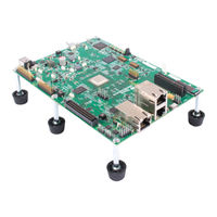
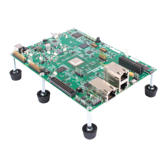
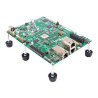
Texas Instruments AM64 Series User Manual (62 pages)
GP EVM
Brand:
Texas Instruments
| Category:
Computer Hardware
| Size: 8 MB
Table of Contents
Table of Contents
1
1 Introduction
3
EVM Revisions and Assembly Variants
4
2 Important Usage Notes
4
Power-On Usage Note
4
Table 1-1. Am64X/Am243X GP EVM PCB Design Revisions, and Asssembly Variants
4
6 Revision History
5
Figure 3-1. Top View of the Am64X/Am243X GP EVM Board
5
Key Features
6
Figure 3-2. Bottom View of the Am64X/Am243X GP EVM Board
6
Functional Block Diagram
8
Diagram
8
Power-On/Off Procedures
9
Power-On Procedure
9
Power-Off Procedure
10
Peripheral and Major Component Description
11
Am64X/Am243X Clock
11
Clocking
11
Ethernet PHY Clock
11
Figure 3-4. Am64X/Am243X GP EVM Clock Tree
11
Pcie Clock
11
Table 3-1. Source Clock Selection for the Clock Buffer
11
Figure 3-5. Overall Reset Architecture of the Am64X/Am243X GP EVM
12
Reset
12
Current Monitoring
13
Power
13
Power Input
13
Reverse Polarity Protection
13
Table 3-2. VMAIN LED
13
Table 3-3. INA Devices I2C Slave Address
13
Power Supply
14
Table 3-4. Power Test Points
14
Figure 3-6. Power Good Leds
15
Table 3-5. Power Leds
15
Figure 3-7. Power on and off Sequencing
16
Power Sequencing
16
Am64X/Am243X Power
17
Figure 3-8. Am64X/Am243X Core Supply and Array Core Supply Options
17
Boot Modes
18
Configuration
18
Table 3-6. Soc Power Supply
18
Figure 3-10. Am64X/Am243X GP EVP PCB, Boot Mode Selection Switches (SW2, SW3)
19
Figure 3-9. Am64X/Am243X GP EVM Schematic Excerpt, Boot Mode Selection Switches (SW2, SW3)
19
Table 3-7. BOOTMODE Bits
20
Table 3-8. PLL Reference Clock Selection BOOTMODE[2:0]
20
Table 3-9. Boot Device Selection BOOTMODE[6:3]
20
Table 3-10. Primary Boot Media Configuration BOOTMODE[9:7]
21
Table 3-11. Backup Boot Mode Selection BOOTMODE[12:10]
21
Table 3-12. Backup Boot Media Configuration BOOTMODE[13]
21
Jtag
22
Table 3-13. Selection of HSE Connector and JTAG TRACE Functionality
22
Table 3-14. TI20 Pin Connector (J25) Pin-Out
22
Figure 3-11. JTAG Interface
23
Table 3-15. TI 60-Pin Connector (J33) Pin-Out
24
Table 3-16. List of Signals Routed to Test Automation Header
25
Test Automation
25
Figure 3-12. Test Automation Header
26
Table 3-17. Test Automation Header (J38) Pin-Out
27
Figure 3-13. Am64X/Am243Xuart Interfaces
28
UART Interfaces
28
DDR4 Interface
29
Figure 3-14. Am64X/Am243X DDR4 Interface
29
Memory Interfaces
29
Figure 3-15. Micro SD Interface
30
MMC Interfaces
30
Figure 3-16. Emmc Interface
31
OSPI Interface
31
Board ID EEPROM Interface
32
Figure 3-17. Am64X/Am243X OSPI Interface
32
SPI EEPROM Interface
32
Table 3-18. Board ID Memory Header Information
32
Ethernet Interface
33
Figure 3-18. Ethernet Interface - CPSW Domain
33
Figure 3-19. Ethernet Interface - ICSSG Domain
34
DP83867 PHY Default Configuration
35
DP83869 PHY Default Configuration
35
Table 3-19. Default Strap Setting of CPSW Ethernet PHY
36
Table 3-20. Default Strap Setting of ICSSG Ethernet Phys
36
Figure 3-20. Am64X/Am243Xethernet Interfaces - CPSW Ethernet Strap Settings
39
Figure 3-21. Am64X/Am243X Ethernet Interfaces - ICSSG1 Ethernet Strap Settings
40
Figure 3-22. Am64X/Am243X Ethernet Interfaces - ICSSG2 Ethernet Strap Settings
41
Ethernet LED
42
Figure 3-23. Am64X/Am243X GP EVM Ethernet Interface LED
42
Display Interface
43
Table 3-21. Display Connector (J36) Pin-Out
43
Figure 3-24. Am64X/Am243X USB 2.0 Host Interface
44
Pcie Interface
44
USB 2.0 Interface
44
Figure 3-25. Am64X/Am243X Pcie Interface
45
Table 3-22. Pcie Jumper Options to Enable Root Complex and Endpoint Mode
45
Table 3-23. Pcie Connector (J27) Pin-Out
45
High Speed Expansion Interface
46
Table 3-24. Selection of PRG0 Signals on Application Connector
47
Figure 3-26. Am64X/Am243X High Speed Expansion Connector
52
Figure 3-27. Am64X/Am243X High Speed Expansion Connector - Part 1
53
CAN Interface
54
Figure 3-28. Am64X/Am243X High Speed Expansion Connector - Part 2
54
Table 3-25. CAN (J31 and J32) Pin-Out
54
ADC Interface
55
Figure 3-29. Am64X/Am243X CAN Interfaces
55
Interrupt
55
Table 3-26. ADC Connector (J3) Pin-Out
55
I2C Interfaces
56
Safety Connector
56
SPI Interfaces
56
Table 3-27. Safety Connector Pinouts
56
Table 3-28. I2C Test Header (J5) Pin-Out
56
Figure 3-30. Am64X/Am243X I2C Interfaces and Address Assignment of Peripherals
57
Table 3-29. I2C Test Header (J4) Pin-Out
57
Figure 3-31. Am64X/Am243X FSI Interface
58
FSI Interface
58
Table 3-30. FSI (J5) Connector Pin-Out
58
4 Known Issues and Modifications
59
Issue 1 - Embedded XDS110 Connection to Am64X Target in CCS
59
Figure 4-1. Am64X/Am243X GP EVM Modification Label Location
59
Table 4-1. Am64X/Am243X GP EVM Known Issues and Modifications
59
Figure 4-2. XDS110 CCS Connection Error Dialog
60
Figure 4-3. XDS110 Debug Reset Utility Command-Line Function
60
Advertisement
Texas Instruments AM64 Series User Manual (56 pages)
Brand:
Texas Instruments
| Category:
Motherboard
| Size: 7 MB
Table of Contents
Table of Contents
1
1 Introduction
3
6 Revision History
4
2 Important Usage Notes
4
Power-On Usage Note
4
Figure 3-1. Top View of General Processor Board
4
Key Features
5
Figure 3-2. Bottom View of General Processor Board
5
Functional Block Diagram
7
Figure 3-3. General Processor Board Functional Block
7
Diagram
7
Power-On/Off Procedures
8
Power-On Procedure
8
Power-Off Procedure
9
Peripheral and Major Component Description
10
Clocking
10
Am64X Soc Clock
10
Ethernet PHY Clock
10
Figure 3-4. Am64X GP EVM Clock Tree
10
Pcie Clock
10
Table 3-1. Source Clock Selection for the Clock Buffer
10
Reset
11
Power
12
Current Monitoring
12
Power Input
12
Reverse Polarity Protection
12
Evm
12
Table 3-2. VMAIN LED
12
Table 3-3. INA Devices I2C Slave Address
12
Power Supply
13
Table 3-4. Power Test Points
13
Figure 3-6. Power Good Leds
14
Table 3-5. Power Leds
14
Figure 3-7. Power on and off Sequencing
15
Power Sequencing
15
Figure 3-8. Core Supply and Array Core Supply Options
16
Table 3-6. Soc Power Supply
16
Boot Modes
17
Configuration
17
Figure 3-10. Am64X GP EVP PCB, Boot Mode Selection Switches (SW2, SW3)
18
Figure 3-9. Am64X GP EVM Schematic Excerpt, Boot Mode Selection Switches (SW2, SW3)
18
Table 3-7. BOOTMODE Bits
19
Table 3-8. PLL Reference Clock Selection BOOTMODE[2:0]
19
Table 3-9. Boot Device Selection BOOTMODE[6:3]
19
Table 3-10. Primary Boot Media Configuration BOOTMODE[9:7]
20
Table 3-11. Backup Boot Mode Selection BOOTMODE[12:10]
20
Table 3-12. Backup Boot Media Configuration BOOTMODE
20
Jtag
21
Table 3-13. Selection of HSE Connector and JTAG TRACE Functionality
21
Table 3-14. TI20 Pin Connector (J25)
21
Figure 3-11. JTAG Interface
22
Table 3-15. TI 60-Pin Connector (J33) Pin-Out
22
Table 3-16. List of Signals Routed to Test Automation Header
23
Test Automation
23
Figure 3-12. Test Automation Header
24
Table 3-17. Test Automation Header (J38) Pin-Out
25
Figure 3-13. UART Interface
26
UART Interface
26
DDR4 Interface
27
Figure 3-14. DDR4 Interface
27
Memory Interfaces
27
Figure 3-15. Micro SD Interface
28
MMC Interface
28
Figure 3-16. Emmc Interface
29
OSPI Interface
29
Board ID EEPROM Interface
30
Figure 3-17. OSPI Interface
30
SPI EEPROM Interface
30
Table 3-18. Board ID Memory Header Information
30
Ethernet Interface
31
Figure 3-18. Ethernet Interface - CPSW Domain
31
Figure 3-19. Ethernet Interface - ICSSG Domain
32
DP83867 PHY Default Configuration
33
DP83869 PHY Default Configuration
33
Table 3-19. Default Strap Setting of CPSW Ethernet PHY
34
Table 3-20. Default Strap Setting of ICSSG Ethernet Phys
34
Figure 3-20. Ethernet Interface - CPSW Ethernet Strap
36
Figure 3-21. Ethernet Interface - ICSSG1 Ethernet Strap Settings
37
Figure 3-22. Ethernet Interface - ICSSG2 Ethernet Strap Settings
38
Ethernet Leds
39
Figure 3-23. GP Board Ethernet Interface - Leds
39
Display Interface
40
Table 3-21. Display Connector (J36) Pin-Out
40
Figure 3-24. USB 2.0 Host Interface
41
Pcie Interface
41
USB 2.0 Interface
41
Figure 3-25. Pcie Interface
42
Table 3-22. Pcie Jumper Options to Enable Root Complex and Endpoint Mode
42
Table 3-23. Pcie Connector (J27) Pin-Out
42
High Speed Expansion Interface
43
Table 3-24. Selection of PRG0 Signals on Application Connector
43
Figure 3-26. High Speed Expansion Connector
45
Figure 3-27. High Speed Expansion Connector Part 1
46
CAN Interface
47
Figure 3-28. High Speed Expansion Connector Part 2
47
Table 3-25. CAN (J31 and J32) Pin-Out
47
ADC Interface
48
Figure 3-29. CAN Interface
48
Interrupt
48
Table 3-26. ADC Connector (J3) Pin-Out
48
I2C Interface
49
Safety Connector
49
SPI Interface
49
Table 3-27. Safety Connector Pinouts
49
Table 3-28. I2C Test Header (J5) Pin-Out
49
Table 3-29. I2C Test Header (J4) Pin-Out
50
Figure 3-30. I2C Interfaces and Address Assignment to Its Peripherals
51
Figure 3-31. FSI Interface
52
FSI Interface
52
Table 3-30. FSI (J5) Connector Pin-Out
52
Soc Power
16
4 Known Issues and Modifications
53
Issue 1 - Embedded XDS110 Connection to Am64X Target in CCS
53
Figure 4-1. Am64X GP EVM Modification Label
53
Table 4-1. Am64X GP EVM Known Issues and Modifications
53
Figure 4-2. XDS110 CCS Connection Error Dialog
54
Figure 4-3. : XDS110 Debug Reset Utility Command-Line Function
54
Issue 2 - MDIO Ethernet PHY Communications
55
Advertisement
Related Products
Texas Instruments AM64 GP EVM Series
Texas Instruments AM6442
Texas Instruments AM64x
Texas Instruments AM64 SK EVM Series
Texas Instruments AM625
Texas Instruments AM623
Texas Instruments AM625SIP
Texas Instruments AM654 Series
Texas Instruments AM62L
Texas Instruments AM625-Q1
Texas Instruments Categories
Motherboard
Control Unit
Microcontrollers
Computer Hardware
Calculator
More Texas Instruments Manuals
Login
Sign In
OR
Sign in with Facebook
Sign in with Google
Upload manual
Upload from disk
Upload from URL