Sign In
Upload
Manuals
Brands
Silicon Laboratories Manuals
Microcontrollers
EFM8SB2
Silicon Laboratories EFM8SB2 Manuals
Manuals and User Guides for Silicon Laboratories EFM8SB2. We have
1
Silicon Laboratories EFM8SB2 manual available for free PDF download: Reference Manual
Silicon Laboratories EFM8SB2 Reference Manual (285 pages)
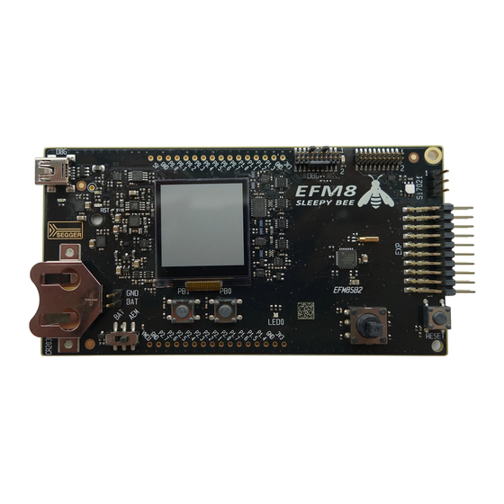
EFM8 Sleepy Bee Family
Brand:
Silicon Laboratories
| Category:
Microcontrollers
| Size: 1 MB
Table of Contents
1 System Overview
2
Introduction
2
Power
3
I/O
3
Clocking
3
Counters/Timers and PWM
4
Communications and Other Digital Peripherals
5
Analog
6
Reset Sources
8
Debugging
8
Bootloader
8
2 Memory Organization
9
Program Memory
9
Data Memory
9
Memory Map
11
3 Special Function Registers
15
Special Function Register Access
15
Special Function Register Memory Map
16
SFR Access Control Registers
21
SFRPAGE: SFR Page
21
4 Flash Memory
22
Introduction
22
Features
24
Functional Description
25
Security Options
25
Programming the Flash Memory
26
Flash Lock and Key Functions
26
Flash Page Erase Procedure
26
Flash Byte Write Procedure
26
Flash Write and Erase Precautions
27
Minimizing Flash Read Current
28
Scratchpad
28
Flash Control Registers
29
PSCTL: Program Store Control
29
FLKEY: Flash Lock and Key
30
FLSCL: Flash Scale
30
5 Device Identification
31
Unique Identifier
31
6 Interrupts
32
Introduction
32
Interrupt Sources and Vectors
32
Interrupt Priorities
32
Interrupt Latency
32
Interrupt Summary
33
Interrupt Control Registers
35
IE: Interrupt Enable
35
IP: Interrupt Priority
37
EIE1: Extended Interrupt Enable 1
39
EIP1: Extended Interrupt Priority 1
41
EIE2: Extended Interrupt Enable 2
43
EIP2: Extended Interrupt Priority 2
44
7 Power Management and Internal Regulators
45
Introduction
45
Features
46
Idle Mode
46
Stop Mode
46
Suspend Mode
47
Sleep Mode
48
Configuring Wakeup Sources
48
Determining the Event that Caused the Last Wakeup
49
Power Management Control Registers
49
PCON0: Power Control 0
49
PMU0CF: Power Management Unit Configuration
50
REG0CN: Voltage Regulator Control
51
8 Clocking and Oscillators
52
Introduction
52
Features
52
Functional Description
52
Clock Selection
52
LPOSC0 20 Mhz Internal Oscillator
52
HFOSC0 24.5 Mhz Internal Oscillator
52
RTC0 Oscillator
53
External Crystal
54
External RC and C Modes
56
External CMOS
58
Clocking and Oscillator Control Registers
59
CLKSEL: Clock Select
59
HFO0CAL: High Frequency Oscillator Calibration
60
HFO0CN: High Frequency Oscillator Control
60
XOSC0CN: External Oscillator Control
61
9 Real Time Clock (RTC0)
62
Introduction
62
Features
62
Functional Description
62
Interface
62
Clocking Options
64
Timer and Alarm
67
RTC Control Registers
68
RTC0KEY: RTC Lock and Key
68
RTC0ADR: RTC Address
69
RTC0DAT: RTC Data
69
RTC0CN0: RTC Control 0
70
RTC0XCN0: RTC Oscillator Control 0
72
RTC0XCF: RTC Oscillator Configuration
73
CAPTURE0: RTC Timer Capture 0
73
CAPTURE1: RTC Timer Capture 1
74
CAPTURE2: RTC Timer Capture 2
74
CAPTURE3: RTC Timer Capture 3
74
ALARM0: RTC Alarm Programmed Value 0
75
ALARM1: RTC Alarm Programmed Value 1
75
ALARM2: RTC Alarm Programmed Value 2
75
ALARM3: RTC Alarm Programmed Value 3
76
RTC0PIN: RTC Pin Configuration
76
10 Reset Sources and Power Supply Monitor
77
Introduction
77
Features
77
Functional Description
78
Device Reset
78
Power-On Reset
79
Supply Monitor Reset
80
External Reset
80
Missing Clock Detector Reset
80
Comparator (CMP0) Reset
80
PCA Watchdog Timer Reset
81
Flash Error Reset
81
Software Reset
81
RTC Reset
81
Reset Sources and Supply Monitor Control Registers
82
RSTSRC: Reset Source
82
VDM0CN: VDD Supply Monitor Control
83
11 Microcontroller Core
84
Introduction
84
Features
85
Functional Description
85
Programming and Debugging Support
85
Instruction Set
86
CPU Core Registers
89
DPL: Data Pointer Low
89
DPH: Data Pointer High
90
SP: Stack Pointer
90
ACC: Accumulator
90
B: B Register
91
PSW: Program Status Word
92
12 Port I/O, Crossbar, External Interrupts, and Port Match
93
Introduction
93
Features
93
Functional Description
94
Port I/O Modes of Operation
94
Pin Drive Strength
95
Analog and Digital Functions
95
Port I/O Analog Assignments
95
Port I/O Digital Assignments
96
Priority Crossbar Decoder
97
Crossbar Functional Map
98
INT0 and INT1
100
Port Match
100
Direct Port I/O Access (Read/Write)
100
Port I/O Control Registers
101
XBR0: Port I/O Crossbar 0
101
XBR1: Port I/O Crossbar 1
103
XBR2: Port I/O Crossbar 2
104
P0MASK: Port 0 Mask
105
P0MAT: Port 0 Match
106
P0: Port 0 Pin Latch
107
P0MDIN: Port 0 Input Mode
108
P0MDOUT: Port 0 Output Mode
109
P0SKIP: Port 0 Skip
110
P0DRV: Port 0 Drive Strength
111
P1MASK: Port 1 Mask
112
P1MAT: Port 1 Match
113
P1: Port 1 Pin Latch
114
P1MDIN: Port 1 Input Mode
115
P1MDOUT: Port 1 Output Mode
116
P1SKIP: Port 1 Skip
117
P1DRV: Port 1 Drive Strength
118
P2: Port 2 Pin Latch
119
P2MDIN: Port 2 Input Mode
120
P2MDOUT: Port 2 Output Mode
121
P2SKIP: Port 2 Skip
122
P2DRV: Port 2 Drive Strength
123
INT0 and INT1 Control Registers
125
IT01CF: INT0/INT1 Configuration
125
13 Analog-To-Digital Converter (ADC0)
127
Introduction
127
Features
128
Functional Description
128
Clocking
128
Voltage Reference Options
128
Internal Voltage Reference
128
Precision Voltage Reference
128
Supply or LDO Voltage Reference
128
External Voltage Reference
128
Ground Reference
129
Input Selection
129
Multiplexer Channel Selection
129
Gain Setting
130
Initiating Conversions
130
Input Tracking
130
Burst Mode
133
8-Bit Mode
133
Output Formatting
134
Window Comparator
135
Temperature Sensor
137
Temperature Sensor Calibration
137
ADC0 Control Registers
138
ADC0CN0: ADC0 Control 0
138
ADC0CF: ADC0 Configuration
139
ADC0AC: ADC0 Accumulator Configuration
140
ADC0PWR: ADC0 Power Control
141
ADC0TK: ADC0 Burst Mode Track Time
141
ADC0H: ADC0 Data Word High Byte
141
ADC0L: ADC0 Data Word Low Byte
142
ADC0GTH: ADC0 Greater-Than High Byte
142
ADC0GTL: ADC0 Greater-Than Low Byte
142
ADC0LTH: ADC0 Less-Than High Byte
143
ADC0LTL: ADC0 Less-Than Low Byte
143
ADC0MX: ADC0 Multiplexer Selection
143
REF0CN: Voltage Reference Control
144
TOFFH: Temperature Sensor Offset High
145
TOFFL: Temperature Sensor Offset Low
145
14 Programmable Current Reference (IREF0)
146
Introduction
146
Features
146
Functional Description
146
Overview
146
IREF0 Control Registers
147
IREF0CN0: Current Reference Control 0
147
15 Comparators (CMP0 and CMP1)
148
Introduction
148
Features
148
Functional Description
149
Response Time and Supply Current
149
Hysteresis
149
Input Selection
149
Multiplexer Channel Selection
150
Output Routing
152
CMP0 Control Registers
153
CMP0CN0: Comparator 0 Control 0
153
CMP0MD: Comparator 0 Mode
154
CMP0MX: Comparator 0 Multiplexer Selection
155
CMP1 Control Registers
156
CMP1CN0: Comparator 1 Control 0
156
CMP1MD: Comparator 1 Mode
157
CMP1MX: Comparator 1 Multiplexer Selection
158
16 Cyclic Redundancy Check (CRC0)
159
Introduction
159
Features
159
Functional Description
160
16-Bit CRC Algorithm
160
32-Bit CRC Algorithm
161
Writing to CRC0CN0
162
Using the CRC on a Data Stream
162
Using the CRC to Check Code Memory
162
Bit Reversal
162
CRC0 Control Registers
163
CRC0CN0: CRC0 Control 0
163
CRC0IN: CRC0 Data Input
164
CRC0DAT: CRC0 Data Output
164
CRC0AUTO: CRC0 Automatic Control
164
CRC0CNT: CRC0 Automatic Flash Sector Count
165
CRC0FLIP: CRC0 Bit Flip
165
17 Programmable Counter Array (PCA0)
166
Introduction
166
Features
166
Functional Description
167
Counter / Timer
167
Interrupt Sources
167
Capture/Compare Modules
167
Edge-Triggered Capture Mode
169
Software Timer (Compare) Mode
170
High-Speed Output Mode
171
Frequency Output Mode
172
PWM Waveform Generation
172
To 11-Bit PWM Modes
174
16-Bit PWM Mode
174
Watchdog Timer Mode
175
PCA0 Control Registers
177
PCA0CN0: PCA Control 0
177
PCA0MD: PCA Mode
178
PCA0PWM: PCA PWM Configuration
180
PCA0L: PCA Counter/Timer Low Byte
181
PCA0H: PCA Counter/Timer High Byte
181
PCA0CPM0: PCA Channel 0 Capture/Compare Mode
182
PCA0CPL0: PCA Channel 0 Capture Module Low Byte
183
PCA0CPH0: PCA Channel 0 Capture Module High Byte
183
PCA0CPM1: PCA Channel 1 Capture/Compare Mode
184
PCA0CPL1: PCA Channel 1 Capture Module Low Byte
185
PCA0CPH1: PCA Channel 1 Capture Module High Byte
185
PCA0CPM2: PCA Channel 2 Capture/Compare Mode
186
PCA0CPL2: PCA Channel 2 Capture Module Low Byte
187
PCA0CPH2: PCA Channel 2 Capture Module High Byte
187
PCA0CPM3: PCA Channel 3 Capture/Compare Mode
188
PCA0CPL3: PCA Channel 3 Capture Module Low Byte
189
PCA0CPH3: PCA Channel 3 Capture Module High Byte
189
PCA0CPM4: PCA Channel 4 Capture/Compare Mode
190
PCA0CPL4: PCA Channel 4 Capture Module Low Byte
191
PCA0CPH4: PCA Channel 4 Capture Module High Byte
191
PCA0CPM5: PCA Channel 5 Capture/Compare Mode
192
PCA0CPL5: PCA Channel 5 Capture Module Low Byte
193
PCA0CPH5: PCA Channel 5 Capture Module High Byte
193
18 External Memory Interface (EMIF0)
194
Introduction
194
Features
194
Functional Description
195
Overview
195
Port I/O Configuration
195
EMIF Pin Mapping
195
Multiplexed External Memory Interface
197
Operating Modes
198
Timing
200
Multiplexed Mode
201
EMIF0 Control Registers
204
EMI0CN: External Memory Interface Control
204
EMI0CF: External Memory Configuration
205
EMI0TC: External Memory Timing Control
206
19 Serial Peripheral Interfaces (SPI0 and SPI1)
208
Introduction
208
Features
208
Functional Description
209
Signals
209
Master Mode Operation
210
Slave Mode Operation
210
Clock Phase and Polarity
211
Basic Data Transfer
212
SPI Timing Diagrams
213
SPI0 Control Registers
216
SPI0CFG: SPI0 Configuration
216
SPI0CN0: SPI0 Control
218
SPI0CKR: SPI0 Clock Rate
219
SPI0DAT: SPI0 Data
219
SPI1 Control Registers
220
SPI1CFG: SPI1 Configuration
220
SPI1CN0: SPI1 Control
222
SPI1CKR: SPI1 Clock Rate
223
SPI1DAT: SPI1 Data
223
20 System Management Bus / I2C (SMB0)
224
Introduction
224
Features
224
Functional Description
224
Supporting Documents
224
Smbus Protocol
225
Configuring the Smbus Module
227
Hardware ACK Multimaster and Multislave Behavior
232
Operational Modes
233
SMB0 Control Registers
241
SMB0CF: Smbus 0 Configuration
241
SMB0CN0: Smbus 0 Control
242
SMB0ADR: Smbus 0 Slave Address
243
SMB0ADM: Smbus 0 Slave Address Mask
244
SMB0DAT: Smbus 0 Data
244
21 Timers (Timer0, Timer1, Timer2, and Timer3)
245
Introduction
245
Features
245
Functional Description
246
System Connections
246
Timer 0 and Timer 1
246
Operational Modes
247
Timer 2 and Timer 3
250
16-Bit Timer with Auto-Reload
252
8-Bit Timers with Auto-Reload (Split Mode)
253
Capture Mode
254
Timer 0, 1, 2 and 3, Control Registers
255
CKCON0: Clock Control 0
255
TCON: Timer 0/1 Control
257
TMOD: Timer 0/1 Mode
258
TL0: Timer 0 Low Byte
259
TL1: Timer 1 Low Byte
259
TH0: Timer 0 High Byte
260
TH1: Timer 1 High Byte
260
TMR2CN0: Timer 2 Control
261
TMR2RLL: Timer 2 Reload Low Byte
262
TMR2RLH: Timer 2 Reload High Byte
262
TMR2L: Timer 2 Low Byte
262
TMR2H: Timer 2 High Byte
263
TMR3CN0: Timer 3 Control 0
264
TMR3RLL: Timer 3 Reload Low Byte
265
TMR3RLH: Timer 3 Reload High Byte
265
TMR3L: Timer 3 Low Byte
265
TMR3H: Timer 3 High Byte
266
22 Universal Asynchronous Receiver/Transmitter 0 (UART0)
267
Introduction
267
Features
267
Functional Description
268
Baud Rate Generation
268
Data Format
268
Data Transfer
269
Multiprocessor Communications
269
UART0 Control Registers
270
SCON0: UART0 Serial Port Control
270
SBUF0: UART0 Serial Port Data Buffer
271
23 C2 Debug and Programming Interface
272
Introduction
272
Features
272
Pin Sharing
272
C2 Interface Registers
273
C2ADD: C2 Address
273
C2DEVID: C2 Device ID
273
C2REVID: C2 Revision ID
273
C2FPCTL: C2 Flash Programming Control
274
C2FPDAT: C2 Flash Programming Data
274
Advertisement
Advertisement
Related Products
Silicon Laboratories EFM8SB1-SLSTK2010A
Silicon Laboratories EFM8 Series
Silicon Laboratories EFM8UB1-SLSTK2000A
Silicon Laboratories EFM8BB2-SLSTK2021A
Silicon Laboratories EFM8SB2-SLSTK2011A
Silicon Laboratories EFM8BB3-SLSTK2022A
Silicon Laboratories EFM32
Silicon Laboratories EFM32 EFM32GG11 Giant Gecko Series
Silicon Laboratories EFM32GG11-SLSTK3701A
Silicon Laboratories EFM32GG-STK3700
Silicon Laboratories Categories
Motherboard
Microcontrollers
Computer Hardware
Control Unit
Transceiver
More Silicon Laboratories Manuals
Login
Sign In
OR
Sign in with Facebook
Sign in with Google
Upload manual
Upload from disk
Upload from URL