Sign In
Upload
Manuals
Brands
Quanmax Manuals
Motherboard
MITX-DNV0 Series
Quanmax MITX-DNV0 Series Motherboard Manuals
Manuals and User Guides for Quanmax MITX-DNV0 Series Motherboard. We have
1
Quanmax MITX-DNV0 Series Motherboard manual available for free PDF download: User Manual
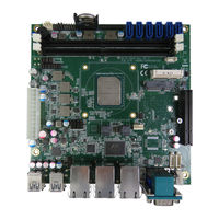
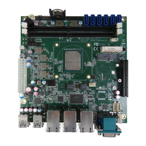
Quanmax MITX-DNV0 Series User Manual (84 pages)
Brand:
Quanmax
| Category:
Motherboard
| Size: 2.58 MB
Table of Contents
Symbols
6
For Your Safety
7
High Voltage Safety Instructions
7
Special Handling and Unpacking Instruction
7
Lithium Battery Precautions
8
General Instructions on Usage
8
Quality and Environmental Management
8
Disposal and Recycling
8
WEEE Compliance
8
Table of Contents
9
List of Tables
10
List of Figures
11
1 / Introduction
13
2 / Installation Procedures
14
Installing the Board
14
Chassis Safety Standards
15
Lithium Battery Replacement
15
3 / System Specifications
17
System Block Diagram
17
Figure 1: System Block Diagram MITX-DNV0 Series
17
Component Main Data
18
Table 1: Component Main Data
18
Environmental Conditions
19
Standards and Certifications
19
Processor Support
19
Table 2: Environmental Conditions
19
Table 3: Standards and Certifications
19
Table 4: Processor Support
19
System Memory Support
20
Memory Operating Frequencies
20
On-Board Graphics Subsystem
20
Table 5: Memory Operating Frequencies
20
Power Supply
21
Table 6: Display Configuration
21
Table 7: Supply Voltages
21
4 / Connector Locations
22
Top Side
22
Table 8: Jumper List
22
Table 9: Top Side Internal Connector Pin Assignment
22
Figure 2: Top Side
22
Connector Panel Side
24
Table 10: Connector Panel Side Connector List
24
Figure 3: Connector Panel Side
24
5 / Connector Definitions
25
6 / I/O-Area Connectors
26
VGA Connector (CN24)
26
Table 11: Pin Assignment VGA Connector CN24
26
Figure 4: VGA Connector CN24
26
Ethernet Connectors (CN18, CN19 & CN20)
27
Table 12: Pin Assignment Ethernet Connectors CN18, CN19, CN20
27
Figure 5: Ethernet Connectors CN18, CN19, CN20
27
USB Connectors (I/O Area)
28
Table 13: Pin Assignment USB3.0 / USB2.0 Connector CN22, CN23
28
Figure 6: USB 3.0 Connector CN22, CN23
28
Table 14: Signal Description
29
Figure 7: USB 2.0 High Speed Cable
29
Figure 8: USB 3.0 High Speed Cable
29
RS232/422/485 COM1 Connector (CN26)
30
Table 15: Pin Assignment RS232/422/485 COM1 Connector CN26
30
Table 16: Signal Description
30
Figure 9: RS232/422/485 COM1 Connector CN26
30
7 / Internal Connectors
31
Power Input Wafer (ATX1)
31
Table 17: Pin Assignment ATX1
31
Figure 10: Power Input Wafer ATX1
31
Table 18: Signal Description
32
CPU / System Fan Wafer (FAN1 & FAN2)
33
Table 19: 4-Pin Mode FAN1, FAN2
33
Table 20: 3-Pin Mode FAN1, FAN2
33
Table 21: Signal Description
33
Figure 11: CPU / System Fan Wafer FAN1, FAN2
33
SATA (Serial ATA) Port 1 ~ Port 6 Connector (SATA1 ~ SATA6)
34
Table 22: Pin Assignment SATA1 ~ SATA6
34
Table 23: Signal Description
34
Figure 12: SATA Port 1 ~ Port 6 Connector SATA1 ~ SATA6
34
USB Connectors (Internal) (CN17)
35
Table 24: Pin Assignment CN5
35
Table 25: Signal Description
35
Figure 13: USB 2.0 Port 1, 2 Pin Header CN17
35
Front Panel Pin Header (FP1 & FP2)
36
Table 26: Pin Assignment FP1
36
Table 27: Signal Description
36
Table 28: Pin Assignment FP2
36
Figure 14: Front Panel 1 Pin Header FP1
36
Figure 15: Front Panel 2 Pin Header FP2
36
Table 29: Signal Description
37
Serial COM2 Ports (CN16)
38
Table 30: Pin Assignment CN16
38
Table 31: Signal Description
38
Figure 16: Serial COM CN16
38
Digital Input / Output Wafer (CN15)
40
Table 32: Pin Assignment CN15
40
Figure 17: Digital Input / Output Wafer CN15
40
PS/2 Keyboard and Mouse Wafer (CN21)
41
Table 33: Pin Assignment CN21
41
Table 34: Signal Description
41
Figure 18: PS/2 Keyboard / Mouse Wafer CN21
41
Key-B SSD Slot (M2B1)
42
Table 35: Pin Assignment CON1
42
Figure 19: M.2 Key-B SSD Slot M2B1
42
Mpcie / Msata Socket (MPCIE1)
45
Table 36: Pin Assignment MPCIE1
45
Figure 20: Mpcie Socket MPCIE1
45
SIM Interface Wafer for MPCIE1 (CN4)
47
Table 37: Pin Assignment CN4
47
Figure 21: SIM Interface Wafer CN4
47
PCIE X8 Socket (PCIE1)
48
Table 38: Pin Assignment PCIE1
48
Figure 22: PCIE X8 Socket PCIE1
48
Gbe LAN LED Header (CN2)
50
Table 39: Pin Assignment CN2
50
Figure 23: Gbe LAN LED Header CN2
50
Wireless Activity LED Header for MPCIE1 (CN5)
51
General Purpose LED Wafer (CN25)
51
Table 40: Pin Assignment CN5
51
Table 41: Pin Assignment CN25
51
Figure 24: Wireless Activity LED Header CN5
51
Figure 25: General Purpose LED Wafer CN25
51
Figure 26: Programming Example 1
52
Figure 27: Programming Example 2
52
Switches and Jumpers
53
Mpcie / Msata Selection for MPCIE1 (JP1)
53
USB Power Selection (JP2)
53
Table 42: Pin Assignment JP1
53
Table 43: Pin Assignment JP2
53
Figure 28: Jumper Connector
53
Figure 29: Mpcie / Msata Selection JP1
53
Figure 30: USB Power Selection JP2
53
AT / ATX Power Mode Selection (JP3)
54
MFG Mode Selection (JP5)
54
Clear CMOS Selection (JP10)
54
Table 44: Pin Assignment JP3
54
Table 45: Pin Assignment JP5
54
Figure 31: at / ATX Power Mode Selection JP3
54
Figure 32: MFG Mode Selection JP5
54
Figure 33: Clear CMOS Selection JP10
54
Flash Security Override Selection (JP11)
55
Power Output Selection for COM1 Pin-9 (JP15)
55
Table 46: Pin Assignment JP10
55
Table 47: Pin Assignment JP11
55
Table 48: Pin Assignment JP15
55
Figure 34: Flash Security Override Selection JP11
55
Figure 35: Power Output Selection JP15
55
8 / Bios
57
Starting the Uefi BIOS
57
Table 49: Font Size Table
57
Setup Menus
58
Main Setup Menu
58
Table 50: Main Setup Menu Sub-Screens and Functions
58
Figure 36: BIOS Main Menu Screen System Data and Time
59
Advanced Setup Menu
60
Figure 37: BIOS Advanced Menu
61
Figure 38: BIOS Advanced Menu - FIA HSIO12 Configuration
62
Figure 39: BIOS Advanced Menu - CPU Chipset Configuration
64
Figure 40: BIOS Advanced Menu - SATA Configuration
65
Figure 41: BIOS Advanced Menu - USB Configuration
66
Figure 42: BIOS Advanced Menu - Trsted Computing
67
Figure 43: BIOS Advanced Menu - Network Stack Configuration
68
Figure 44: BIOS Advanced Menu - DIO Configuration
69
Figure 45: BIOS Advanced Menu - Super IO Configuration
70
Figure 46: BIOS Advanced Menu - Super IO Configuration - Serial Port 1 Configuration
70
Figure 47: BIOS Advanced Menu - Super IO Configuration - Serial Port 2 Configuration
71
Figure 48: BIOS Advanced Menu - Serial Port Console Redirection
72
Figure 49: BIOS Advanced Menu - Serial Port Console Redirection - COM1 / COM2 Console Redirection Settings
73
Figure 50: BIOS Advanced Menu - Serial Port Console Redirection - Legacy Console Redirection Settings
74
Figure 51: BIOS Advanced Menu - Serial Port Console Redirection - Out-Of-Band Mgmt Port Console Redirection Settings
75
Figure 52: BIOS Advanced Menu - H/W Monitor
76
Power Setup Menu
77
Figure 53: BIOS Power Setup Menu
77
Figure 54: BIOS Power Setup Menu - Watchdog Timer Configuration
78
Boot Setup Menu
79
Figure 55: BIOS Boot Setup Menu
79
Security Setup Menu
80
Figure 56: BIOS Boot Setup Menu
80
Remember the Password
81
Save & Exit Setup Menu
82
Figure 57: BIOS Boot Setup Menu
82
Appendix A: List of Acronyms
83
Table 51: List of Acronyms
83
About Quanmax
84
Advertisement
Advertisement
Related Products
Quanmax MITX-SLS0/KLS0 Series
Quanmax MITX-V1K0 Series
Quanmax QBox Mini-1000 Series
Quanmax MoniQ-1500
Quanmax MoniQ-1700
Quanmax MoniQ-1900
Quanmax Qbox Mini-2000 Series
Quanmax ATX-KLS0 Series
Quanmax ECX-KLU0 Series
Quanmax ECX-SLU0 Series
Quanmax Categories
Desktop
Touch Panel
Motherboard
Computer Hardware
Monitor
More Quanmax Manuals
Login
Sign In
OR
Sign in with Facebook
Sign in with Google
Upload manual
Upload from disk
Upload from URL