Sign In
Upload
Manuals
Brands
Orsys Manuals
Motherboard
MICRO-LINE C6713Compact-2
Orsys MICRO-LINE C6713Compact-2 Manuals
Manuals and User Guides for Orsys MICRO-LINE C6713Compact-2. We have
1
Orsys MICRO-LINE C6713Compact-2 manual available for free PDF download: Hardware Reference Manual
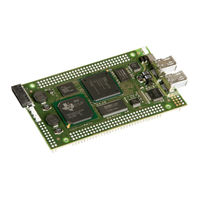
Orsys MICRO-LINE C6713Compact-2 Hardware Reference Manual (65 pages)
Brand:
Orsys
| Category:
Motherboard
| Size: 1 MB
Table of Contents
Table of Contents
2
Preface
6
History
7
Hardware Overview
8
Block Diagram of the C6713Compact-2
8
Connectors
9
Micro-Line Connector
9
JTAG Connector
10
IEEE1394 Connectors
10
Interfaces and Hardware Components
10
Fpga
10
IEEE1394 Interface
12
External Memory (On-Board SDRAM)
12
Block Diagram of the IEEE1394 Interface
12
Flash Memory
13
DDR3 Memory
13
Pld
13
UART / RS-232 Interface
13
Serial EEPROM
13
Temperature Sensor
14
Reset Generator and Watchdog
14
External Flags (XF Signals)
14
Power Supply of the Board
14
Status Led's
15
User Programmable Led's (PLD)
15
User Programmable Led's (FPGA)
15
IEEE1394 Status Led's
15
DSP Peripherals
15
Multichannel Audio Serial Ports (Mcasp)
16
External Memory Interface (EMIF)
16
Inter Integrated Circuit
16
Interfaces
16
General Purpose Input / Output Peripheral (GPIO)
17
Multi-Channel Buffered Serial Ports (Mcbsp)
17
Timers
17
Host Port Interface (HPI)
18
Interrupts
18
Dma
19
C6713Compact-2 Interrupt Routing
19
Memory Maps and Description of the Registers
20
TMS320C6713 Memory Map
20
Memory Map of the TMS320C6713 DSP
20
C6713Compact-2 Address Map
21
Doc. No. : C6713Cpt-2_Hrg
21
Iss./Rev : 1.0
21
MICRO - LINE ® C6713Compact-2
21
Internal RAM
21
DSP Peripherals
21
External RAM
21
Flash Memory
21
Memory Map of the C6713Compact-2
21
Endianness
22
EMIF Configuration
22
Default EMIF Configuration
22
Description of the Board Registers
23
Description of the PLD Registers
25
Hardware Configuration Register (HWCFG)
25
Flash Segment Register (FSR)
26
FPGA Control Register (FCR)
27
Red LED Source Select Register (LEDSRC)
27
Module Control Register (MCR)
28
UART Registers
28
I 2 C Bus Control Register (I2C)
30
External Flag Register (XF)
30
Watchdog Enable and Phy Reset Register (WDG_PHRST)
31
UART Clock Control Register (UART_CLK)
31
Version Register (VERSION)
32
EXT_INT6 Enable and Line Status Register (EXT_INT6_EN_ST)
32
Version Register Encoding
32
EXT_INT7 Enable Register (EXT_INT7_EN)
33
EXT_INT7 Line Status Register (EXT_INT7_ST)
33
Boot Process and Default Setup of the C6713Compact-2
35
Using the Flash File System
36
Flash File System Commands
36
Software Development Support
37
Description of the Micro-Line ® Board Connectors
38
Location of the Connectors
38
Connector Overview
39
Pinout Tables of the Micro-Line ® Connector
39
Pinout of Connectors A, B, BB, C, D and E
39
Pinout of Connectors P, X, Alternative 1394 Port 1 & 2 and EGND
40
Pinout Summary for the Mcbsp Interfaces
40
Pinout Summary for the Timers
40
Pinout Summary for the I2C Interfaces
41
Pinout of the JTAG Connector
42
Pinout of the IEEE1394 Connectors
43
Function of the Pins
43
Connector a
43
Connector B
43
MICRO - LINE ® C6713Compact-2
43
Connector BB
43
IEEE1394 Connector Pin Assignment
43
IEEE1394 Connector Socket; Front View
43
Connector D
44
Connector E
45
Connector P
50
Connector X
50
EGND Connector
51
Environment
52
Minimal Connections
52
Changing the Board Configuration
53
Location of the Components
53
Component Locations for Configuration (Top Side)
53
Component Locations for Configuration (Bottom Side)
53
Factory Default Configuration
54
Configuring Micro-Line ® Pin E16 Termination
54
Configuring Micro-Line ® Pin D30 Termination
54
Configuring for HPI or Mcasp Usage
54
Factory Default Configuration Summary
54
Configuring the IEEE1394 Power Supply
55
Configuring the IEEE1394 Cable Shield
55
Configuring for Using the Alternative IEEE1394 Connectors
55
Block Diagram of the IEEE1394 Interface
55
Configuring the DSP Clock Frequency
56
Configuring for Micro-Line ® Master or Slave Usage
56
Board Stack Example Where the C6713Compact-2 Is Configured as Master
56
Configuring the Default State of the FPGA I/O Pins
57
Configuring Board Supply Voltage
57
Board Stack Example Where the C6713Compact-2 Is Configured as Slave
57
Signal Levels and Loads
58
Input Voltage Levels for Non-FPGA Signals
58
Output Voltage Levels for Non-FPGA Signals
58
Signal Levels for FPGA Signals
58
Allowed Loads
58
Supply Voltage
58
Power Consumption
59
Reset Timing
59
Ambient Temperature
59
Ambient Humidity
59
Power Consumption of the C6713Compact-2
59
Dimensions of the Board
60
Dimensions of the C6713Compact-2 (in Millimeters)
60
Complete Micro-Line ® Footprint
61
Spare Micro-Line Connectors
62
Differences between C6713Compact and C6713Compact-2
63
Main Differences between C6713Compact and C6713Compact-2
63
Reference Documents
64
List of Abbreviations Used in this Document
65
ARDWARE EFERENCE UIDE Doc. No. : C6713Cpt-2_Hrg
65
Iss./Rev : 1.0
65
MICRO LINE C6713Compact-2
65
Advertisement
Advertisement
Related Products
Orsys micro-line C6713CPU
Orsys Categories
Computer Hardware
Motherboard
More Orsys Manuals
Login
Sign In
OR
Sign in with Facebook
Sign in with Google
Upload manual
Upload from disk
Upload from URL