Table of Contents
Advertisement
Quick Links
Date
: 11 April 2012
H
R
G
ARDWARE
EFERENCE
UIDE
Doc. no. : C6713Cpt-2_hrg
®
Iss./Rev : 1.0
-
C6713Compact-2
MICRO
LINE
Page
: 1
Hardware Reference Guide
®
micro-line
C6713Compact-2
High performance DSP / FPGA / IEEE 1394 board
,
Orsys Orth System GmbH, Am Stadtgraben 25, 88677 Markdorf
Germany
http://www.orsys.de
Advertisement
Table of Contents

Summary of Contents for Orsys MICRO-LINE C6713Compact-2
- Page 1 EFERENCE UIDE Doc. no. : C6713Cpt-2_hrg ® Iss./Rev : 1.0 C6713Compact-2 MICRO LINE Page Hardware Reference Guide ® micro-line C6713Compact-2 High performance DSP / FPGA / IEEE 1394 board Orsys Orth System GmbH, Am Stadtgraben 25, 88677 Markdorf Germany http://www.orsys.de...
-
Page 2: Table Of Contents
Date : 11 April 2012 ARDWARE EFERENCE UIDE Doc. no. : C6713Cpt-2_hrg ® Iss./Rev : 1.0 C6713Compact-2 MICRO LINE Page Contents 1 PREFACE........................6 History ............................. 7 2 HARDWARE OVERVIEW ..................... 8 Block Diagram of the C6713Compact-2 ................8 Connectors ..........................9 ®... - Page 3 Date : 11 April 2012 ARDWARE EFERENCE UIDE Doc. no. : C6713Cpt-2_hrg ® Iss./Rev : 1.0 C6713Compact-2 MICRO LINE Page Internal RAM ......................... 21 DSP Peripherals ........................21 External RAM ........................21 Flash Memory ........................21 Endianness ........................... 22 EMIF Configuration ......................22 3.8.1 Default EMIF configuration....................
- Page 4 Date : 11 April 2012 ARDWARE EFERENCE UIDE Doc. no. : C6713Cpt-2_hrg ® Iss./Rev : 1.0 C6713Compact-2 MICRO LINE Page 7.6.3 Connector BB ........................43 7.6.4 Connector D ........................44 7.6.5 Connector E ........................45 7.6.6 Connector P ........................50 7.6.7 Connector X ........................
- Page 5 Date : 11 April 2012 ARDWARE EFERENCE UIDE Doc. no. : C6713Cpt-2_hrg ® Iss./Rev : 1.0 C6713Compact-2 MICRO LINE Page List of tables PLD interrupt sources of the C6713Compact-2 ................18 Memory map of the TMS320C6713 DSP..................20 Memory map of the C6713Compact-2 .................... 21 default initialization values for the FPGA related CE space registers ..........
-
Page 6: Preface
FPGA design loaded. Additional features are available through board support packages (BSP's). They use a FPGA design that implements these features. Please contact ORSYS for a list of available board support packages. The FPGA of the C6713Compact-2 can be used either with board support packages from ORSYS or with custom designs using the FPGA development option. -
Page 7: History
Date : 11 April 2012 ARDWARE EFERENCE UIDE Doc. no. : C6713Cpt-2_hrg ® Iss./Rev : 1.0 C6713Compact-2 MICRO LINE Page 1.1 History Revision Changes First public release, adapted from C6713Compact with the following changes: references to FFS v3 removed section explaining FPGA loading revised temperature sensor resolution modified to sensor's native resolution data file access from user application mentioned GPIO usage for polling interrupt state mentioned... -
Page 8: Hardware Overview
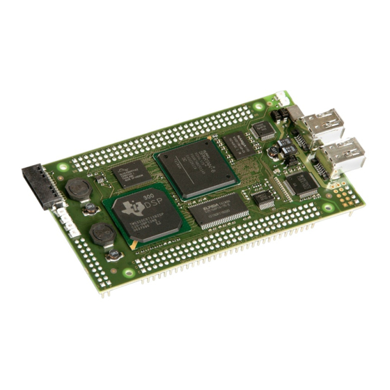
Date : 11 April 2012 ARDWARE EFERENCE UIDE Doc. no. : C6713Cpt-2_hrg ® Iss./Rev : 1.0 C6713Compact-2 MICRO LINE Page 2 Hardware Overview 2.1 Block Diagram of the C6713Compact-2 Figure 1: Block diagram of the C6713Compact-2... -
Page 9: Connectors
Date : 11 April 2012 ARDWARE EFERENCE UIDE Doc. no. : C6713Cpt-2_hrg ® Iss./Rev : 1.0 C6713Compact-2 MICRO LINE Page Flash FPGA DDR3 UART memory memory IEEE1394 port active LED (yellow) JTAG emulator LLC status LED connector red LED (FPGA) green LED (FPGA) IEEE1394 red LED... -
Page 10: Jtag Connector
The FPGA on the C6713Compact-2 can be used for a predefined application using one of the board support packages provided by ORSYS, or it can be programmed by the user to any customized design by using the FPGA development package. Using FPGA technology allows ®... - Page 11 Date : 11 April 2012 ARDWARE EFERENCE UIDE Doc. no. : C6713Cpt-2_hrg ® Iss./Rev : 1.0 C6713Compact-2 MICRO LINE Page : 11 The FPGA has access to the following signal groups: • DSP EMIF (data bus, address bus, control signals) •...
-
Page 12: Ieee1394 Interface
Date : 11 April 2012 ARDWARE EFERENCE UIDE Doc. no. : C6713Cpt-2_hrg ® Iss./Rev : 1.0 C6713Compact-2 MICRO LINE Page : 12 2.3.2 IEEE1394 Interface The C6713Compact-2 uses the Texas Instruments TSB12LV32 general purpose link layer controller (LLC) and a TSB41AB2 physical layer transceiver (Phy). This chipset provides •... -
Page 13: Flash Memory
Date : 11 April 2012 ARDWARE EFERENCE UIDE Doc. no. : C6713Cpt-2_hrg ® Iss./Rev : 1.0 C6713Compact-2 MICRO LINE Page : 13 2.3.4 Flash Memory The C6713Compact-2 uses an S29GL064 (8Mbyte) or an S29GL256 (32Mbyte) flash memory for non-volatile storage. The flash memory is 16 bit wide and can hold up to 32Mbytes of data. It is used for permanent storage of application code. -
Page 14: Temperature Sensor
2.3.12 Power Supply of the Board Nominal supply voltage for the C6713Compact-2 is 5 V. If 3.3 V supply is required, please contact Orsys. For operation of the IEEE1394 interface, an additional supply voltage of 8…30 V is required which can be provided over the IEEE1394 cable or locally. -
Page 15: Status Led's
Date : 11 April 2012 ARDWARE EFERENCE UIDE Doc. no. : C6713Cpt-2_hrg ® Iss./Rev : 1.0 C6713Compact-2 MICRO LINE Page : 15 The following voltages are generated internally on the C6713Compact-2: • 1.4 V supply voltage for the processor core •... -
Page 16: Multichannel Audio Serial Ports (Mcasp)
The EMIF can be used to access external hardware by using an appropriate FPGA design. This can be either a board support package from ORSYS, or a custom FPGA design. The EMIF is mapped into the DSP's address space, separated into four categories, or CE spaces: •... -
Page 17: General Purpose Input / Output Peripheral (Gpio)
Date : 11 April 2012 ARDWARE EFERENCE UIDE Doc. no. : C6713Cpt-2_hrg ® Iss./Rev : 1.0 C6713Compact-2 MICRO LINE Page : 17 2.5.4 General Purpose Input / Output Peripheral (GPIO) On the C6713Compact-2 board, usage of the GPIO peripheral is not recommended, since there ®... -
Page 18: Host Port Interface (Hpi)
On the C6713Compact-2 board, the host port is only available with an appropriate FPGA design, thus by using either an appropriate board support package from ORSYS, or a custom FPGA design. The HPI function of shared signals is enabled by default (by both, the DSP, and default hardware configuration of the C6713Compact-2 (see chapter 8.2). -
Page 19: Dma
Date : 11 April 2012 ARDWARE EFERENCE UIDE Doc. no. : C6713Cpt-2_hrg ® Iss./Rev : 1.0 C6713Compact-2 MICRO LINE Page : 19 Figure 6: C6713Compact-2 interrupt routing Using the interrupt lines with the alternative GPIO function is not recommended except for polling the state of an interrupt line. -
Page 20: Memory Maps And Description Of The Registers
Date : 11 April 2012 ARDWARE EFERENCE UIDE Doc. no. : C6713Cpt-2_hrg ® Iss./Rev : 1.0 C6713Compact-2 MICRO LINE Page : 20 3 Memory Maps and Description of the Registers 3.1 TMS320C6713 Memory Map The memory map of the TMS320C6713 is divided into several sections: •... -
Page 21: C6713Compact-2 Address Map
Date : 11 April 2012 ARDWARE EFERENCE UIDE Doc. no. : C6713Cpt-2_hrg ® Iss./Rev : 1.0 C6713Compact-2 MICRO LINE Page : 21 3.2 C6713Compact-2 Address Map The table below shows how the C6713Compact-2 uses the four CE address spaces of the processor. -
Page 22: Endianness
Date : 11 April 2012 ARDWARE EFERENCE UIDE Doc. no. : C6713Cpt-2_hrg ® Iss./Rev : 1.0 C6713Compact-2 MICRO LINE Page : 22 memory is divided into 32 segments, each of them holds 1Mbyte of data. The current segment that can be accessed is selected by the flash segment register described in chapter 3.10. The flash memory can be programmed in units of sectors, each of 64Kbyte size. -
Page 23: Description Of The Board Registers
Date : 11 April 2012 ARDWARE EFERENCE UIDE Doc. no. : C6713Cpt-2_hrg ® Iss./Rev : 1.0 C6713Compact-2 MICRO LINE Page : 23 CE space configuration register 32 bit initialization value 5675 D923 5675 D913 Table 4: default initialization values for the FPGA related CE space registers parameter value Timing for an EMIF clock of... - Page 24 Date : 11 April 2012 ARDWARE EFERENCE UIDE Doc. no. : C6713Cpt-2_hrg ® Iss./Rev : 1.0 C6713Compact-2 MICRO LINE Page : 24 base register name register mnemonic address 9011 0000h hardware configuration register (read-only) HWCFG 9012 0000h Flash Segment register 9013 0000h FPGA control register 9014 0000h...
-
Page 25: Description Of The Pld Registers
Date : 11 April 2012 ARDWARE EFERENCE UIDE Doc. no. : C6713Cpt-2_hrg ® Iss./Rev : 1.0 C6713Compact-2 MICRO LINE Page : 25 base register name register mnemonic address LLC_ASYNRETRY 901F 004Ch LLC asynchronous retry (16 / 32 bit) LLC_ATFFIRST 901F 0050h LLC ATF first (16 / 32 bit) LLC_ATFCONT 901F 0054h... -
Page 26: Flash Segment Register (Fsr)
Date : 11 April 2012 ARDWARE EFERENCE UIDE Doc. no. : C6713Cpt-2_hrg ® Iss./Rev : 1.0 C6713Compact-2 MICRO LINE Page : 26 bit 7 bit 6 bit 5 bit 4 bit [3:0] RAMSIZE CPUSPEED HPI_EN BUSMASTER RESERVED r, 0 RAMSIZE RAMSIZE SDRAM size 32 MB... -
Page 27: Fpga Control Register (Fcr)
Date : 11 April 2012 ARDWARE EFERENCE UIDE Doc. no. : C6713Cpt-2_hrg ® Iss./Rev : 1.0 C6713Compact-2 MICRO LINE Page : 27 bit[7:3] bit [2:0] SEGMENT RESERVED r,w,00000 3.10.3 FPGA Control Register (FCR) The FPGA control register is used by application software to load code into the FPGA. Details on FPGA loading can be found in the application examples that are delivered together with the C6713Compact-2. -
Page 28: Module Control Register (Mcr)
Date : 11 April 2012 ARDWARE EFERENCE UIDE Doc. no. : C6713Cpt-2_hrg ® Iss./Rev : 1.0 C6713Compact-2 MICRO LINE Page : 28 3.10.5 Module Control Register (MCR) bit 7 bit 6 bit 5 bit 4 bit 3 bit [2:0] SW_RESET LED_RED CTSRESET_CTL LED_GREEN RS232_DRV_CTL RESERVED r,w,0... - Page 29 Date : 11 April 2012 ARDWARE EFERENCE UIDE Doc. no. : C6713Cpt-2_hrg ® Iss./Rev : 1.0 C6713Compact-2 MICRO LINE Page : 29 address DLAB bit in LCR = 0 DLAB bit in LCR = 1 mnemonic access type mnemonic access type 9016 0000 read only read/write...
-
Page 30: I 2 C Bus Control Register (I2C)
Date : 11 April 2012 ARDWARE EFERENCE UIDE Doc. no. : C6713Cpt-2_hrg ® Iss./Rev : 1.0 C6713Compact-2 MICRO LINE Page : 30 3.10.7 I C Bus Control Register (I2C) The on-board temperature sensor with its 256 byte EEPROM is connected to the PLD by a local C-bus interface (none of the DSP's I C interfaces is used). -
Page 31: Watchdog Enable And Phy Reset Register (Wdg_Phrst)
Date : 11 April 2012 ARDWARE EFERENCE UIDE Doc. no. : C6713Cpt-2_hrg ® Iss./Rev : 1.0 C6713Compact-2 MICRO LINE Page : 31 3.10.9 Watchdog Enable and Phy Reset Register (WDG_PHRST) This register controls the polarity of bit 7 bit 6 bit 5 bit 4 bit [3:0]... -
Page 32: Version Register (Version)
Date : 11 April 2012 ARDWARE EFERENCE UIDE Doc. no. : C6713Cpt-2_hrg ® Iss./Rev : 1.0 C6713Compact-2 MICRO LINE Page : 32 CLK_EN CLK_SEL UART_CLK High-Z (UART_CLK is not driven) 3.6864 MHz 11.0592 MHz Table 10: Possible configurations for UARTCLK 3.10.11 Version Register (VERSION) This register contains a version number which depends on the C6713Compact-2 version. -
Page 33: Ext_Int7 Enable Register (Ext_Int7_En)
Date : 11 April 2012 ARDWARE EFERENCE UIDE Doc. no. : C6713Cpt-2_hrg ® Iss./Rev : 1.0 C6713Compact-2 MICRO LINE Page : 33 3.10.12.1 Why the Interrupt Line Status is Needed Since there are multiple interrupt sources for EXT_INT6, it is important know, where the interrupt came from in order to take the appropriate action. - Page 34 Date : 11 April 2012 ARDWARE EFERENCE UIDE Doc. no. : C6713Cpt-2_hrg ® Iss./Rev : 1.0 C6713Compact-2 MICRO LINE Page : 34 UART If this bit is set to 1, the UART has an interrupt pending. UART interrupts can be used by software drivers for the UART.
-
Page 35: Boot Process And Default Setup Of The C6713Compact-2
Date : 11 April 2012 ARDWARE EFERENCE UIDE Doc. no. : C6713Cpt-2_hrg ® Iss./Rev : 1.0 C6713Compact-2 MICRO LINE Page : 35 4 Boot Process and Default Setup of the C6713Compact-2 After reset or power up the C6713Compact-2 boots the Flash File System from flash memory. The Flash File System sets up clock and EMIF settings of the TMS320C6713 DSP (see table below). -
Page 36: Using The Flash File System
Date : 11 April 2012 ARDWARE EFERENCE UIDE Doc. no. : C6713Cpt-2_hrg ® Iss./Rev : 1.0 C6713Compact-2 MICRO LINE Page : 36 5 Using the Flash File System The C6713Compact-2 is always shipped with the Flash File System installed. The Flash File System manages the storage of application software and FPGA designs. -
Page 37: Software Development Support
C6713Compact-2. The micro-line board library is described in detail in [22]. Furthermore Orsys provides various development support packages like DSP Development Kit or DCAM Frame Capture Development Kit. These kits are described in corresponding kit user’s guides. The DSP Development Kit for example is described in [23]. These kit user’s guides contain... -
Page 38: Description Of The Micro-Line ® Board Connectors
Date : 11 April 2012 ARDWARE EFERENCE UIDE Doc. no. : C6713Cpt-2_hrg ® Iss./Rev : 1.0 C6713Compact-2 MICRO LINE Page : 38 7 Description of the micro-line Board Connectors ® 7.1 Location of the Connectors For the micro-line connectors, Pin 1 is marked by a square shape in Figure 9. Note: By default, the alternative IEEE1394 connectors are not mounted and the EGND connector uses only 4 pins. -
Page 39: Connector Overview
Date : 11 April 2012 ARDWARE EFERENCE UIDE Doc. no. : C6713Cpt-2_hrg ® Iss./Rev : 1.0 C6713Compact-2 MICRO LINE Page : 39 7.2 Connector Overview ® This table below gives an overview, how the micro-line connector is used on previous CPU and peripheral boards. -
Page 40: Pinout Of Connectors P, X, Alternative 1394 Port 1 & 2 And Egnd
Date : 11 April 2012 ARDWARE EFERENCE UIDE Doc. no. : C6713Cpt-2_hrg ® Iss./Rev : 1.0 C6713Compact-2 MICRO LINE Page : 40 Connector alt. 1394 alt. 1394 EGND port 1 port 0 N.C. (FPGA) TPA1+ TPA0+ ESD GND N.C. (FPGA) TPA1- TPA0- ESD GND... -
Page 41: Pinout Summary For The I2C Interfaces
Date : 11 April 2012 ARDWARE EFERENCE UIDE Doc. no. : C6713Cpt-2_hrg ® Iss./Rev : 1.0 C6713Compact-2 MICRO LINE Page : 41 signal shared with connected to interface signal SCL0 N.C. SDA0 N.C. ® SCL1 McBSP CLKS1 micro-line connector E16 ®... -
Page 42: Pinout Of The Jtag Connector
Date : 11 April 2012 ARDWARE EFERENCE UIDE Doc. no. : C6713Cpt-2_hrg ® Iss./Rev : 1.0 C6713Compact-2 MICRO LINE Page : 42 7.4 Pinout of the JTAG Connector signal signal used for FPGA_TMS FPGA FPGA_TDI FPGA_TDO FPGA_TCK +3.3 V not connected not connected unused CPU_EMU0... -
Page 43: Pinout Of The Ieee1394 Connectors
Date : 11 April 2012 ARDWARE EFERENCE UIDE Doc. no. : C6713Cpt-2_hrg ® Iss./Rev : 1.0 C6713Compact-2 MICRO LINE Page : 43 7.5 Pinout of the IEEE1394 Connectors Figure 11: IEEE1394 connector socket; front view signal description cable power supply +8..30 V cable ground TBP- differential pair B... -
Page 44: Connector D
Date : 11 April 2012 ARDWARE EFERENCE UIDE Doc. no. : C6713Cpt-2_hrg ® Iss./Rev : 1.0 C6713Compact-2 MICRO LINE Page : 44 Pins BB17 though BB32: These signals are routed to the FPGA. Usage of these signals requires either a board support package or a custom FPGA design. -
Page 45: Connector E
Date : 11 April 2012 ARDWARE EFERENCE UIDE Doc. no. : C6713Cpt-2_hrg ® Iss./Rev : 1.0 C6713Compact-2 MICRO LINE Page : 45 RTS: This pin is the ready to send output of the RS-232 interface. Output voltage is either -5.5 V (typical) or +5.5 V (typical). - Page 46 Date : 11 April 2012 ARDWARE EFERENCE UIDE Doc. no. : C6713Cpt-2_hrg ® Iss./Rev : 1.0 C6713Compact-2 MICRO LINE Page : 46 This pin is connected to the DSP over a 22Ω series resistor. How to use it is described in [3], [5] and [6].
- Page 47 Date : 11 April 2012 ARDWARE EFERENCE UIDE Doc. no. : C6713Cpt-2_hrg ® Iss./Rev : 1.0 C6713Compact-2 MICRO LINE Page : 47 CLKS1 / SCL1: This pin has a dual function: • If configured for McBSP usage, this pin is the external input of the internal sample rate generator used for McBSP 1.
- Page 48 Date : 11 April 2012 ARDWARE EFERENCE UIDE Doc. no. : C6713Cpt-2_hrg ® Iss./Rev : 1.0 C6713Compact-2 MICRO LINE Page : 48 • If configured for McASP usage, this pin is the receive high-frequency master clock of McASP 0. This pin is connected to the DSP over a 22Ω series resistor. How to use it is described in [3], [5] and [6].
- Page 49 Date : 11 April 2012 ARDWARE EFERENCE UIDE Doc. no. : C6713Cpt-2_hrg ® Iss./Rev : 1.0 C6713Compact-2 MICRO LINE Page : 49 FSR0 / AFSR0: This pin has a dual function: • If configured for McBSP usage, this pin is the receiver frame sync output or input of McBSP 0.
-
Page 50: Connector P
Date : 11 April 2012 ARDWARE EFERENCE UIDE Doc. no. : C6713Cpt-2_hrg ® Iss./Rev : 1.0 C6713Compact-2 MICRO LINE Page : 50 TOUT1 / AXR0[4]: This pin has a dual function: • If configured for timer usage, this pin is the output of timer 1. The timer output can e.g. trigger an external A/D converter to start a conversion. -
Page 51: Egnd Connector
Date : 11 April 2012 ARDWARE EFERENCE UIDE Doc. no. : C6713Cpt-2_hrg ® Iss./Rev : 1.0 C6713Compact-2 MICRO LINE Page : 51 regulator is required). This pin should not be used to supply power to the IEEE1394 cable. Instead, the +8..30 V pin should be used in conjunction with the appropriate board hardware configuration (see chapter 8.2). -
Page 52: Environment
Date : 11 April 2012 ARDWARE EFERENCE UIDE Doc. no. : C6713Cpt-2_hrg ® Iss./Rev : 1.0 C6713Compact-2 MICRO LINE Page : 52 8 Environment 8.1 Minimal Connections ® This chapter shows how to set up the C6713Compact-2 for use without a micro-line Power Supply carrier board. -
Page 53: Changing The Board Configuration
Date : 11 April 2012 ARDWARE EFERENCE UIDE Doc. no. : C6713Cpt-2_hrg ® Iss./Rev : 1.0 C6713Compact-2 MICRO LINE Page : 53 8.2 Changing the Board Configuration This chapter shows how to change the board configuration by placing/replacing board components and closing / opening solder bridges. -
Page 54: Factory Default Configuration
Date : 11 April 2012 ARDWARE EFERENCE UIDE Doc. no. : C6713Cpt-2_hrg ® Iss./Rev : 1.0 C6713Compact-2 MICRO LINE Page : 54 8.2.2 Factory Default Configuration The table below shows a summary of all configurable settings and their factory default. Many of them can be configured by the user whereas a few of them are only available as factory configuration. -
Page 55: Configuring The Ieee1394 Power Supply
Date : 11 April 2012 ARDWARE EFERENCE UIDE Doc. no. : C6713Cpt-2_hrg ® Iss./Rev : 1.0 C6713Compact-2 MICRO LINE Page : 55 R117 McASP GPIO[0,1,3,8..15] enabled disabled disabled mounted with 0Ω (default) not mounted disabled enabled enabled 8.2.6 Configuring the IEEE1394 Power Supply By default, IEEE1394 cable power can supply the IEEE1394 transceiver of the C6713Compact-2, but local power can't be supplied to the IEEE1394 cable. -
Page 56: Configuring The Dsp Clock Frequency
Date : 11 April 2012 ARDWARE EFERENCE UIDE Doc. no. : C6713Cpt-2_hrg ® Iss./Rev : 1.0 C6713Compact-2 MICRO LINE Page : 56 CAUTION: When using the alternative IEEE1394 connectors, the signals must be routed according to the rules defined in [21]; (paragraph 4.2.1.4.1) in order to guarantee signal integrity. 8.2.9 Configuring the DSP Clock Frequency The C6713Compact-2 is shipped with a TMS320C6713B, running at 300MHz. -
Page 57: Configuring The Default State Of The Fpga I/O Pins
Configuration for master or slave usage is a factory configuration which is not available to the user, but is part of some BSP's or can be done by ORSYS on request. Application software can the current setting from the PLD HWCFG register, BUSMASTER bit (see chapter 3.10.1). -
Page 58: Signal Levels And Loads
Nominal supply voltage for the C6713Compact-2 is +5 V DC. The integrated switched power supplies generate the required voltages for the board. If 3.3 V supply is required, please contact Orsys. CAUTION: The C6713Compact-2 is not protected against reversed voltage. Please be careful when... -
Page 59: Power Consumption
Date : 11 April 2012 ARDWARE EFERENCE UIDE Doc. no. : C6713Cpt-2_hrg ® Iss./Rev : 1.0 C6713Compact-2 MICRO LINE Page : 59 Board type minimum allowed supply voltage maximum allowed supply voltage C6713Compact-2 4.5 V 5.5 V Table 23: Voltage limits for the C6713Compact-2 8.5 Power Consumption The typical power consumption is shown in the following table. -
Page 60: Dimensions Of The Board
Date : 11 April 2012 ARDWARE EFERENCE UIDE Doc. no. : C6713Cpt-2_hrg ® Iss./Rev : 1.0 C6713Compact-2 MICRO LINE Page : 60 8.9 Dimensions of the Board All dimensions are in millimeters. Board height is 5mm (measured from top side of the PCB), with exception of the IEEE1394 connectors, which have a height of 8.7mm. -
Page 61: Complete Micro-Line ® Footprint
Date : 11 Ap ril 2012 ARDWARE EFERENCE UIDE Doc. no. : C671 3Cpt-2_hrg ® Iss./Rev : 1.0 C6713Compact-2 MICRO LINE Page : 61 78,74 5.71 5.71 2.54 5.71 5.71 15,24 17.78 17.78 ® Figure 20: Complete micro-line footprint... -
Page 62: Spare Micro-Line Connectors
Date : 11 April 2012 ARDWARE EFERENCE UIDE Doc. no. : C6713Cpt-2_hrg ® Iss./Rev : 1.0 C6713Compact-2 MICRO LINE Page : 62 ® 8.10 Spare micro-line Connectors For customized hardware designs, standard 0.100 inch square post sockets as well as PC104 type connectors can be used. -
Page 63: Differences Between C6713Compact And C6713Compact-2
Date : 11 April 2012 ARDWARE EFERENCE UIDE Doc. no. : C6713Cpt-2_hrg ® Iss./Rev : 1.0 C6713Compact-2 MICRO LINE Page : 63 9 Differences between C6713Compact and C6713Compact-2 The C6713Compact-2 is quite similar to its predecessor, the C6713Compact. Below is a list of the main differences: Feature C6713Compact... -
Page 64: Reference Documents
S29GL-N MirrorBit® Flash Family S29GL-N_01 S29GL-N_00 [21] , IEEE, IEEE Standard for a High Performance Serial Bus 1394-1995 [22] , Orsys, C6713Compact-2 Board Library User’s Guide C6713cpt_Boardlib_ug [23] , Orsys, C6713Compact-2 DSP Development Kit User’s Guide C6713cpt_DSP_DevKit_ug [24] , Orsys,... -
Page 65: List Of Abbreviations Used In This Document
Date : 11 April 2012 ARDWARE EFERENCE UIDE Doc. no. : C6713Cpt-2_hrg ® Iss./Rev : 1.0 C6713Compact-2 MICRO LINE Page : 65 11 List of Abbreviations Used in this Document board support package: a combination of software and FPGA design that provides further functionality to the C6713Compact-2 Code Composer Studio –TI's development environment Central Processing Unit = processor...
Need help?
Do you have a question about the MICRO-LINE C6713Compact-2 and is the answer not in the manual?
Questions and answers