Sign In
Upload
Manuals
Brands
Lattice Semiconductor Manuals
Motherboard
iCE40 UltraPlus
Lattice Semiconductor iCE40 UltraPlus Manuals
Manuals and User Guides for Lattice Semiconductor iCE40 UltraPlus. We have
4
Lattice Semiconductor iCE40 UltraPlus manuals available for free PDF download: User Manual, Usage Manual
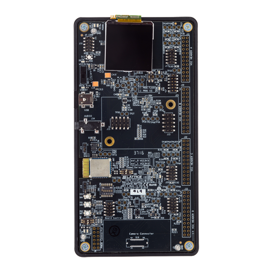
Lattice Semiconductor iCE40 UltraPlus User Manual (44 pages)
Mobile Development Platform
Brand:
Lattice Semiconductor
| Category:
Motherboard
| Size: 1 MB
Table of Contents
Evaluation Board User Guide
1
Table of Contents
2
1 Introduction
4
2 Features
5
Figure 2.1. Ice40 Ultraplus Mobile Development Platform Board (Top Side)
6
Figure 2.2. Ice40 Ultraplus Mobile Development Platform Board (Bottom Side)
7
3 Power and Battery
8
Power Source
8
Current Measurement Test Points
8
Battery Management and 4.2 V Regulator
8
Figure 3.1. Power Block Diagram
8
4 Clock Sources
9
Figure 4.1. Clock Sources for the Ice40 Ultraplus MDP Board
9
5 Software Requirements
10
6 Demonstrations
11
Mobile Display Demonstration on U1
11
Audio Microphone Demonstrations on U2
11
RGB LED Demonstration on U3
11
Sensor Demonstrations on U3
12
Face Recognition Demonstration on U4
12
Figure 6.1. Rework Resistor Positions Described in Parallel Video Bus Configuration
13
7 Board Configuration and Programming
14
Jumpers and Switches
14
Table 7.1. Ice40 Ultraplus Device Selection
14
Figure 7.1. Board Configuration for Programming Ice40 Ultraplus Device "UI
15
Table 7.2. Ice40 Ultraplus Device Selection Summary
16
Programming the Ice40 Devices Configuration Memory (CRAM)
17
Figure 7.2. Programming Ice40 Devices on Board
17
Programming Onboard SPI Flash
18
Figure 7.3. Programming SPI Flash on Board
18
8 Communication Channels
20
Usb
20
Bluetooth
20
9 Ordering Information
20
10 PCB Revision History
20
References
21
Standards Documents
21
Lattice Semiconductor Documents
21
Technical Support Assistance
21
Appendix A. Ice40 Ultraplus Mobile Development Board Schematics
22
Figure A.1. Block Diagram
22
Figure A.2. Ice40Up5K FPGA a - Display
23
Figure A.3. Ice40Up5K FPGA B - Audio
24
Figure A.4. Ice40Up5K FPGA C - Sensor
25
Figure A.5. Ice40Up5K FPGA D - Camera
26
Figure A.6. Common Components- SPI
27
Figure A.7. Display Circuitry
28
Figure A.8. Audio Circuitry
29
Figure A.9. Sensor & RGB Circuitry
30
Figure A.10. Camera Circuitry
31
Figure A.11. USB Programming
32
Figure A.12. Power Supplies
33
Figure A.13. Common Components
34
Figure A.14. Battery Connector & Charger
35
Appendix B. Ice40 Ultraplus Mobile Development Board Bill of Materials
36
Accessories
42
Revision History
43
Advertisement
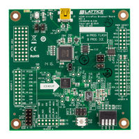
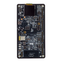
Lattice Semiconductor iCE40 UltraPlus User Manual (36 pages)
Breakout Board
Brand:
Lattice Semiconductor
| Category:
Motherboard
| Size: 1 MB
Table of Contents
Table of Contents
3
Introduction
5
Features
6
Figure 2.1. Ice40 Ultraplus Breakout Board (Top Side)
6
Ice40 Ultraplus Device
7
Software Requirements
8
Demonstration Design Shunts
9
Figure 5.1. Default Shunt Locations
9
Clock Sources
10
Board Power
11
Board Configuration and Programming
12
Figure 8.1. Board Configuration for Programming Flash
12
Figure 8.2. Device Property Settings for Programming Flash
13
Figure 8.3. Setting Status in Diamond Programmer for Programming Flash
13
Figure 8.4. Device Property Settings for Programming Ice40 Ultraplus
14
Test Points
15
Figure 9.1. J52 Header 'A' Breakouts
15
Figure 9.2. J2 Header 'B' Breakouts
15
Figure 9.3. J3 Header 'C' Breakouts
15
Figure 9.4. U6 PMOD Connector
16
Figure 9.5. J1 Adardvark Connector
16
Figure 9.6. Breakout Headers
16
RGB LED Demonstration Design and Software GUI
17
Figure 10.1. SPI Flash Selection (Horizontal) for J6
17
Figure 10.2. Ice40 Ultraplus Selection (Vertical) for J6
18
Figure 10.3. Ice40 Ultraplus LED Demonstration Interface
18
GUI Serial Communication Interface
20
LED Control Via SPI
20
SPI Protocol
20
Figure 11.1. SPI Physical Transaction
20
Table 11.1. Register Address and Bit Field Allocation
20
Table 11.2. Bit Field Functionality Definition
20
Register Definitions
21
Table 11.3. RGB Color Code Definition
21
Table 11.4. LED Brightness Code Definition
21
Table 11.5. Breathe Ramp Code Definition
22
Table 11.6. Blink Rate Code Definition
22
Ordering Information
23
Appendix A. Schematic Diagrams
24
Figure A.1. Block Diagram
24
Figure A.2. FTDI Connection
25
Figure A.3. DUT Connection
26
Figure A.4. RGB,PMOD and HEADERS
27
Figure A.5. Regulator Connection
28
Figure A.6. SPI
29
Appendix B. Bill of Materials
30
References
33
Standards Documents
33
Technical Support Assistance
33
Revision History
34
Lattice Semiconductor iCE40 UltraPlus User Manual (15 pages)
Sensor Data Buffer with BLE - Radiant Software
Brand:
Lattice Semiconductor
| Category:
Accessories
| Size: 1 MB
Table of Contents
Table of Contents
2
Acronyms in this Document
3
Introduction
4
Functional Description
4
Figure 2.2. Ice40 Ultraplus Sensor Data Buffer with BLE Demo Block Diagram
4
Demo Setup
5
Hardware Requirements
5
Software and Firmware Requirements
5
Figure 3.1. Android Phone with Jelly Bean 4.3 or Kitkat 4.4 and the Ice40 Ultraplus MDP
5
Configuring the MDP Board
6
Setting Jumpers and Switches
6
Figure 3.2. MDP Board Configuration
6
Table 3.1. Detailed Information of the Board Configuration
7
Programming the Demo
8
Programming the Bitmaps to the MDP Board
8
Figure 4.1. Getting Started Dialog Box
8
Figure 4.2. Radiant Programmer Main Interface
8
Figure 4.3. Device Properties Dialog Box
9
Figure 4.4. Program Button
9
Installing the Sensor Data Buffer BLE APK Onto the Android Phone
10
Connecting the Ice40 Ultraplus MDP to the Android Phone
10
Figure 4.5. Activate Bluetooth Prompt
10
Running the Demo
11
Figure 5.1. BLE Device Scan
11
Figure 5.2. Start Demo Button
11
Figure 5.3. Airplane Button
12
Figure 5.4. Successful Operation
13
Figure 5.5. Interface Is Reset
13
Technical Support Assistance
14
Revision History
14
Advertisement
Lattice Semiconductor iCE40 UltraPlus Usage Manual (13 pages)
Oscillator
Brand:
Lattice Semiconductor
| Category:
Computer Hardware
| Size: 0 MB
Table of Contents
Table of Contents
3
Acronyms in this Document
4
Introduction
5
Key Features
5
On-Chip Oscillator Overview
5
Figure 2.1. On-Chip Oscillator
5
I/O Port Description
6
Connectivity Guideline
6
Figure 4.1. Oscillator Calibration Example
6
Table 3.1. SB_HFOSC/HSOSC I/O
6
Table 3.2. SB_LFOSC/LSOSC I/O
6
Figure 4.2. Oscillator Used for Dynamic Clock Calibration that Can be Used on Service LED
7
Power Management Options
8
Appendix A: Design Entry
9
SB_LFOSC Usage in Icecube2 Software
9
SB_HFOSC Usage in Icecube2 Software
9
LSOSC Usage in Lattice Radiant Software
9
HSOSC Usage in Lattice Radiant Software
10
Technical Support Assistance
11
Revision History
12
Advertisement
Related Products
Lattice Semiconductor iCE40 UltraPlus Series
Lattice Semiconductor iCE40LM4K
Lattice Semiconductor iCE40 UltraLite
Lattice Semiconductor iCE40LP8K-USBC-EVN
Lattice Semiconductor iCE40HX-8K
Lattice Semiconductor iCE40UP5K_A
Lattice Semiconductor iCE40UP5K_B
Lattice Semiconductor iCE40UP5K_D
Lattice Semiconductor iCE40UP5K_C
Lattice Semiconductor ICE40HX8K-B-EVN
Lattice Semiconductor Categories
Motherboard
Computer Hardware
Microcontrollers
Controller
Recording Equipment
More Lattice Semiconductor Manuals
Login
Sign In
OR
Sign in with Facebook
Sign in with Google
Upload manual
Upload from disk
Upload from URL