Sign In
Upload
Manuals
Brands
Infineon Manuals
Microcontrollers
MOTIX TLE985xQX
Infineon MOTIX TLE985xQX Motor Driver Manuals
Manuals and User Guides for Infineon MOTIX TLE985xQX Motor Driver. We have
1
Infineon MOTIX TLE985xQX Motor Driver manual available for free PDF download: User Manual
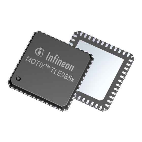
Infineon MOTIX TLE985xQX User Manual (1057 pages)
Arm Cortex-M0 Microcontroller with LIN and H-Bridge NFET Driver for Automotive Applications
Brand:
Infineon
| Category:
Microcontrollers
| Size: 24.25 MB
Table of Contents
Table of Contents
2
Overview
15
Block Diagram
17
General Device Information
18
Pin Configurations
18
Pin Definitions and Functions
19
Modes of Operations
22
Device Register Types
25
Power Management Unit (PMU)
26
Features
26
Introduction
26
Block Diagram
27
PMU Modes Overview
29
Power Supply Generation
35
Voltage Regulator 5.0V (VDDP)
35
Voltage Regulator 1.5V (VDDC)
37
External Voltage Regulator 5.0V (VDDEXT)
38
Power-On Reset Concept
39
PMU Register Overview
40
Register Definition
40
Power Supply Generation Register
40
VDDEXT Control Register
44
Power Control Unit
47
Power Control Unit - Fail Safe Scenarios
47
Power Supervision Function of PCU
47
Watchdog (WDT1) Fail Safe
47
Main Regulators Fail Safe
47
VDDEXT Failure
48
Wake-Up from Stop Mode with Reset Fail Safe
48
Register Definition
50
Wake-Up Management Unit (WMU)
53
Register Definition
55
PMU Wake up Configuration Register
56
PMU Wake up Status Register
61
GPIO Port Wake up Status Register
63
Cyclic Management Unit (CMU)
66
Cyclic Sense Mode
66
Configuration of Cyclic Sense Mode
67
Cyclic Wake Mode
69
Register Definition
69
Cyclic Mode Configuration Registers (CYCMU)
70
Reset Management Unit (RMU)
74
Register Definition
77
Reset Management Unit Registers (RMU)
77
PMU Data Storage Area
81
Register Definition
81
Data Storage Registers
81
System Control Unit - Digital Modules (SCU-DM)
84
Features
84
Introduction
84
Block Diagram
85
SCU Register Overview
87
Register Map
87
Clock Generation Unit
90
Low Precision Clock
90
Clock Control Unit
91
Clock Tree
93
Startup Control for System Clock
94
External Clock Output
94
CGU Registers
95
System Clock Control Registers
96
Analog Peripherals Clock Control Registers
99
External Clock Control Register
112
Reset Control
114
Types of Reset
114
Overview
114
Module Reset Behavior
115
Functional Description of Reset Types
116
Power-On / Brown-Out Reset
116
Wake-Up Reset
116
Hardware Reset
116
WDT1 Reset
116
WDT / Soft Reset
116
Reset Register Description
117
Booting Scheme
118
Power Management
119
Overview
119
Functional Description
120
Slow down Mode
120
Stop Mode
120
Sleep Mode
122
Register Description
123
Interrupt Management
124
Overview
124
External Interrupts
124
Extended Interrupts
125
Interrupt Node Assignment
125
Interrupt Registers
126
Interrupt Node Enable Registers
127
External Interrupt Control Registers
131
Interrupt Flag Registers
134
Interrupt Related Registers
156
Interrupt Event Enable Control
156
NMI Event Flags Handling
163
General Port Control
164
Timer 2/Timer 21 Input Selection Configuration
164
Input Pin Function Selection
165
Port Output Control
171
GPT12 T3IN/T4IN Input Pin Function Selection
177
Differential Unit Trigger Enable
178
Differential Unit Trigger
179
Differential Unit Trigger Register
180
Flexible Peripheral Management
182
Peripheral Management Registers
183
Module Suspend Control
185
Baud-Rate Generator
187
Baudrate Generator Registers
187
Baud-Rate Generator Control and Status Registers
187
Baud-Rate Generator Timer/Reload Registers
189
LIN Break and Sync Byte Detection
194
LIN Break and Sync Byte Detection Control
194
LIN Break and Sync Byte Registers
194
Watchdog Timer
197
Functional Description
198
Register Description
200
Error Detection and Correction Control for Memories
205
Error Detection and Correction Control Register
205
Error Detection and Correction Status Register
207
Miscellaneous Control
210
Bit Protection Register
210
System Control and Status Registers
212
System Control Unit - Power Modules (SCU-PM)
225
Features
225
Introduction
225
Block Diagram
225
Clock Watchdog Unit (CWU)
226
Fail Safe Functionality of Clock Generation Unit (Clock Watchdog)
226
Functional Description of Clock Watchdog Module
227
Clock Generation Unit Register
229
Interrupt Control Unit (ICU)
232
Structure of PREWARN_SUP_NMI
232
Interrupt Control Unit Status Register
234
Interrupt Control Unit Status Overview Register
234
Interrupt Control Unit - Interrupt Clear Register
241
Interrupt Control Unit - Interrupt Enable Register
246
Power Control Unit for Power Modules (PCU_PM)
249
VS-Overvoltage System Shutdown
251
Overtemperature System Shutdown
251
Power Control Unit Register
253
Arm® Cortex®-M0 Core
256
Features
256
Introduction
256
Block Diagram
256
Funtional Description
257
Registers
258
General-Purpose Registers
258
Special-Purpose Registers
258
Summary of Processor Registers
260
Instruction Set Summary
288
Address Space Organization
291
Memory Control Unit
294
Features
294
Introduction
294
Block Diagram
294
NVM Module (Flash Memory)
296
Definitions
296
General Definitions
297
Functional Description
299
Basic Block Functions
299
Memory Cell Array
300
SFR Accesses
301
Memory Read
301
Memory Write
302
Timing
302
Verify
302
Tearing-Safe Programming
302
Disturb Handling
302
ECC and EDC
302
Code and Data Access through the AHB-Lite Interface
303
Bootrom Module
304
Bootrom Addressing
304
Bootrom Firmware Program Structure
304
RAM Module
305
RAM Addressing
305
Memory Protection Unit (MPU)
306
Bootrom
306
Hardware Protection Mode
306
Bootrom Protection Mode
307
NVM Protection Modes
308
Firmware Protection Mode
314
Core Protection Mode
316
Interrupt System
317
Features
317
Introduction
317
Overview
317
Functional Description
318
Interrupt Node Assignment
318
Interrupt Node 0 and 1 - GPT12 Timer Module
318
Interrupt Node 2 - Measurement Unit
319
Interrupt Node 3 - ADC10
320
Interrupt Node 4, 5, 6, 7 - CCU6
321
Interrupt Node 8 and 9 - SSC
322
Interrupt Node 10 - UART1
323
Interrupt Node 11 - UART2
324
Interrupt Node 12 and 13 - Interrupt
325
Interrupt Node 14
326
Interrupt Node 15
326
Interrupt Node 17 and 18 - Bridge Driver / Charge Pump
326
Interrupt Node 19 - HS
327
Interrupt Node 20 - Current Sense Amplifier
327
Interrupt Node 21 - DPP1 Differential Unit
328
Interrupt Node 22 - Monx
328
Interrupt Node 23 - Port2.X
329
Non-Maskable Interrupt Request Source (NMI)
331
Interrupt Flags Overview
332
Interrupt Structure
343
Interrupt Source and Vector
344
Interrupt Priority
347
Interrupt Handling
348
Interrupt Registers
349
Interrupt Node Enable Registers
350
External Interrupt Control Registers
352
Interrupt Flag Registers
355
Interrupt Priority Registers
379
Math Divider Module
380
Features
380
Introduction
380
Block Diagram
380
Divider Unit (DIV)
381
Features
381
Division Operation
381
Start Mode Selection
382
Error Handling
382
Operand/Result Pre-/Post-Processing
384
Global Functions
386
Result Chaining
386
Result Chaining When Start Mode = 0
386
Handling Busy Flags When Result Chaining Is Enabled
386
Service Request Generation
387
Debug Behaviour
387
Enable/ Disable Behaviour
387
Power, Reset and Clock
387
Register Description
389
Math Module Registers
389
Watchdog Timer (WDT1)
404
Features
404
Introduction
405
Functional Description
405
Modes of Operation
405
Normal Operation
406
Watchdog Register Overview
408
GPIO Ports and Peripheral I/O
410
Features
410
Introduction
411
Port 0 and Port 1
411
Port 2
412
Functional Description
413
Register Controlled Functions
413
Data Registers - Pxdata
414
Direction Control- Pxdir
414
Open Drain Control - Pxod
414
Pull-Up/Pull-Down Device - Pxpudsel Pxpuden
414
Alternate Functions Control - Pxaltsel0/1
415
Alternate Functions
416
Port 0 Functions
416
Port 1 Functions
419
Port 2 Functions
421
Register Description
423
Port 0 Register Description
423
Port 1 Register Description
434
Port 2 Register Description
444
General Purpose Timer Units (GPT12)
449
Features
449
Features Block GPT1
449
Features Block GPT2
449
Introduction
449
Block Diagram GPT1
450
Block Diagram GPT2
451
Timer Block GPT1
452
GPT1 Core Timer T3 Control
453
GPT1 Core Timer T3 Operating Modes
455
GPT1 Auxiliary Timers T2/T4 Control
461
GPT1 Auxiliary Timers T2/T4 Operating Modes
462
GPT1 Clock Signal Control
469
Interrupt Control for GPT1 Timers
471
GPT12 Registers
472
GPT1 Registers
472
GPT1 Timer Registers
472
GPT1 Core Timer T3 Control Register
474
GPT1 Auxiliary Timers T2/T4 Control Registers
477
Encoding
480
GPT1 Timer Interrupt Control Registers
482
Timer Block GPT2
483
GPT2 Core Timer T6 Control
484
GPT2 Core Timer T6 Operating Modes
485
GPT2 Auxiliary Timer T5 Control
488
GPT2 Auxiliary Timer T5 Operating Modes
489
GPT2 Register CAPREL Operating Modes
492
GPT2 Clock Signal Control
497
Interrupt Control for GPT2 Timers and CAPREL
498
GPT2 Registers
499
GPT2 Timer Registers
499
GPT2 Timer Control Registers
500
Encoding
504
GPT2 Timer and CAPREL Interrupt Control Registers
505
Miscellaneous GPT12 Registers
506
Implementation of the GPT12 Module
509
Module Connections
509
Timer2 and Timer21
512
Features
512
Introduction
512
Timer2 and Timer21 Modes Overview
513
Functional Description
513
Auto-Reload Mode
513
Up/Down Count Disabled
514
Up/Down Count Enabled
515
Capture Mode
517
Count Clock
517
Interrupt Generation
518
Timer 2 Register Definition
518
Mode Register
519
Control Register
521
Timer 2 Reload/Capture Register
524
Timer 2 Count Register
525
Timer2 and Timer21 Implementation Details
526
Interfaces of the Timer2 and Timer21
526
Capture/Compare Unit 6 (CCU6)
528
Feature Set Overview
528
Introduction
529
Block Diagram
530
Operating Timer T12
531
T12 Overview
532
T12 Counting Scheme
534
Clock Selection
534
Edge-Aligned / Center-Aligned Mode
535
Single-Shot Mode
537
T12 Compare Mode
538
Compare Channels
538
Channel State Bits
538
Hysteresis-Like Control Mode
543
Compare Mode Output Path
544
Dead-Time Generation
544
State Selection
546
Output Modulation and Level Selection
547
T12 Capture Modes
549
T12 Shadow Register Transfer
553
Timer T12 Operating Mode Selection
554
Operating Timer T13
554
T13 Overview
555
T13 Counting Scheme
557
Clock Selection
557
T13 Counting
558
Single-Shot Mode
558
Synchronization to T12
559
T13 Compare Mode
561
Compare Mode Output Path
563
T13 Shadow Register Transfer
564
Trap Handling
566
Multi-Channel Mode
568
Hall Sensor Mode
570
Hall Pattern Evaluation
571
Hall Pattern Compare Logic
573
Hall Mode Flags
573
Hall Mode for Brushless DC-Motor Control
575
Interrupt Handling
577
Interrupt Structure
577
General Module Operation
579
Input Selection
579
CCU6 Register Description
580
System Registers
581
Timer 12 - Related Registers
584
Timer 13 - Related Registers
596
Capture/Compare Control Registers
599
Global Modulation Control Registers
613
Multi-Channel Modulation Control Registers
619
Interrupt Control Registers
625
Tle985Xqx Module Implementation Details
637
Interfaces of the CCU6 Module
637
Uart1/2
639
Features
639
Introduction
639
Block Diagram
640
UART Modes
640
Mode 0, 8-Bit Shift Register, Fixed Baud Rate
640
Mode 1, 8-Bit UART, Variable Baud Rate
641
Mode 2, 9-Bit UART, Fixed Baud Rate
643
Mode 3, 9-Bit UART, Variable Baud Rate
643
Multiprocessor Communication
645
Interrupts
645
Baud Rate Generation
646
Baud-Rate Generator
646
LIN Support in UART
648
LIN Protocol
648
LIN Header Transmission
649
Automatic Synchronization to the Host
650
Initialization of Break/Synch Field Detection Logic
651
Baud-Rate Range Selection
651
LIN Baud Rate Detection
653
Register Description
654
UART Registers
654
Baud-Rate Generator Control and Status Registers
658
Interfaces of the UART Module Mod_Name
659
LIN Transceiver
660
Features
660
Introduction
660
Block Diagram
661
Functional Description
661
LIN Normal Mode
661
LIN Transceiver Error Handling
664
Slope Modes
665
LIN Transceiver Status for Mode Selection
665
LIN Transceiver Slope Mode Status
666
Register Definition
667
LIN Transceiver Interrupts
674
High-Speed Synchronous Serial Interface SSC1/2
675
Features
675
Introduction
675
Block Diagram
676
Functional Description
676
SSC1 and SSC2 Mode Overview
676
Operating Mode Selection
677
Full-Duplex Operation
678
Half-Duplex Operation
681
Continuous Transfers
681
Port Control
682
Baud Rate Generation
683
Error Detection Mechanisms
684
Interrupts
687
SSC Kernel Registers
688
Port Input Select Register
688
Configuration Register
689
Baud Rate Timer Reload Register
694
Transmitter Buffer Register
696
Receiver Buffer Register
696
Output Multiplexing
697
Measurement Unit
698
Features
698
Introduction
698
Block Diagram
699
Measurement Unit Register Overview
700
8-Bit - 10 Channel ADC Core
701
Transfer Characteristics of ADC2
701
ADC2 Measurement Channel- and Control Register Description
701
10-Bit - 14 Channel ADC Core
702
Transfer Characteristics of ADC1
702
Central and Charge Pump Temperature Sensor
703
Supplement Modules
704
Functional Safety Concept
704
Supplement Modules Control and Status Register
705
Measurement Core Module (Incl. ADC2)
707
Features
707
Introduction
707
Block Diagram
708
Measurement Core Module Modes Overview
708
ADC2 - Core (8-Bit ADC)
709
Functional Description
709
ADC2 Control Registers
710
Channel Controller
714
Functional Description
714
Channel Controller Control Registers
716
Calibration Unit
733
Functional Description
733
Method for Determining the Calibration Parameters
733
Setup of Calibration Unit
733
Calibration Unit Control Registers
735
IIR-Filter
740
Functional Description
740
Step Response
741
IIR Filter Control Registers
743
Signal Processing
754
Functional Description
754
Postprocessing Control Registers
757
Start-Up Behavior after Reset
778
Postprocessing Default Values
778
Analog Digital Converter ADC10B (ADC1)
780
Features
780
Introduction
781
Block Diagram
781
ADC1 Modes Overview
781
ADC1 - Core (10-Bit ADC)
783
Functional Description
783
ADC1 Control and Status Registers
784
ADC - Trigger Unit
789
Channel Controller
790
Functional Description
790
Channel Controller Control Registers
793
Calibration Unit
814
Functional Description
814
Method for Determining the Calibration Parameters
814
Setup of Calibration Unit
814
Calibration Unit Control Registers
816
IIR-Filter
824
Functional Description
824
Step Response
825
IIR Filter Control Registers
827
Signal Processing
863
Functional Description
863
Postprocessing Control Registers
865
Interrupt Handling
890
Functional Description
890
Interrupt Registers
897
Differential Measurement Unit
917
Motivation for Differential Measurement Unit
917
Implementation of Differential Measurement Unit
917
ADC1 Differential Unit Input Selection Register
919
Start-Up Behavior after Reset
921
Postprocessing Default Values
922
High-Voltage Monitor Input
923
Features
923
Introduction
923
Block Diagram
923
Functional Description
924
Register Definition
926
Monitor Input Registers
926
High-Side Switch
932
Features
932
Introduction
933
Block Diagram
933
General
933
Functional Description
933
Normal Operation
933
Slew Rate Configuration
934
Overcurrent Detection
934
Overtemperature Detection
934
ON-State Open Load Detection
934
PWM Operation
935
Cyclic Switching in Low Power Mode
935
Register Definition
936
High-Side Switch Register
936
Interrupt Generation - and Status Bit Logic
942
Application Information
943
Bridge Driver (Incl. Charge Pump)
944
Features
944
Introduction
945
Block Diagram
945
Flexible Control
945
Current-Driven Output Stages
946
Overview
946
Switch-On
947
Switch-Off
948
Control Modes
948
Adjustable Cross-Conduction Protection
950
High-Current Discharge Mode
950
Passive Pull-Down Mode
950
Brake Mode
951
Hold Mode
951
Timing Measurements
951
Adaptive Control Mode
952
Integrated 2-Stage Charge Pump
952
Adjustable Voltage Monitoring
953
Adjustable Short Circuit Detection
953
Open-Load Detection
953
Overtemperature
953
Functional Description
953
Flexible Control
953
Current-Driven Output Stages
954
Adjustable Cross-Conduction Protection
957
High-Current Discharge Mode
958
Passive Pull-Down Mode
958
Brake Mode
958
Hold Mode
958
Timing Measurements
958
Fast Comparators
958
Channel Turn On/Off Delay Measurement
959
Adaptive Control Mode
960
Introduction
960
Target Settings
960
Optimizer Activation
961
Monitoring
961
Integrated 2-Stage Charge Pump
961
Clock Generator of Driver Supply
961
Adjustable Voltage Monitoring
962
Adjustable Short-Circuit Detection
962
Overtemperature
962
Register Definition
963
Driver Register
965
Sequencer Configuration Registers
983
Half Bridge 1 - Slew Rate Configuration Registers for Switch-Off/On
984
Half Bridge 1 - Slew Rate Configuration Registers for Active Freewheeling
990
Half Bridge 2 - Slew Rate Configuration Registers for Switch-Off/On
992
Half Bridge 2 - Slew Rate Configuration Registers for Active Freewheeling
997
Adaptive Slew Rate Sequencer Control and Status Registers
999
Adaptive Slew Rate Sequencer Configuration Registers
1005
Driver Trimming Register
1022
Charge Pump Control and Status Register
1025
Dynamic Compensation Trimming Register
1036
Current Sense Amplifier
1038
Features
1038
Introduction
1038
Block Diagram
1039
Functional Description
1039
ADC Code Calculation
1040
Register Definition
1041
Application Information
1043
Window-Lift Application Diagram
1043
Connection of Unused Pins
1045
Connection of P0.2 for SWD Debug Mode
1045
Connection of TMS
1045
ESD Tests
1045
Revision History
1047
Advertisement
Advertisement
Related Products
Infineon TLE985 Series
Infineon TLE984 Series
Infineon TLE984 QX Series
Infineon TLE9842QX
Infineon TLE9842-2QX
Infineon TLE9843QX
Infineon TLE9843-2QX
Infineon TLE9844QX
Infineon TLE9844-2QX
Infineon TLE9845QX
Infineon Categories
Motherboard
Microcontrollers
Computer Hardware
Control Unit
Controller
More Infineon Manuals
Login
Sign In
OR
Sign in with Facebook
Sign in with Google
Upload manual
Upload from disk
Upload from URL