Sign In
Upload
Manuals
Brands
GOWIN Manuals
Semiconductors
DK_START_GW2AR-LV18EQ144PC8I7
GOWIN DK_START_GW2AR-LV18EQ144PC8I7 Manuals
Manuals and User Guides for GOWIN DK_START_GW2AR-LV18EQ144PC8I7. We have
1
GOWIN DK_START_GW2AR-LV18EQ144PC8I7 manual available for free PDF download: User Manual
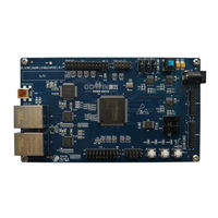
GOWIN DK_START_GW2AR-LV18EQ144PC8I7 User Manual (33 pages)
Brand:
GOWIN
| Category:
Semiconductors
| Size: 1 MB
Table of Contents
Table of Contents
4
List of Figures
6
About this Guide
8
Purpose
8
Related Documents
8
Abbreviations and Terminology
8
Support and Feedback
9
Table 1-1 Abbreviations and Terminologies
9
Development Board Description
10
Overview
10
Figure 2-1 DK_START_GW2AR-LV18EQ144PC8I7_V1.1 Development Board
10
A Development Board Suite
11
Figure 2-2 a Development Board Kit
11
PCB Components
12
System Architecture
12
Figure 2-3 PCB Components
12
Figure 2-4 System Architecture
12
Features
13
Development Board Specification
14
Table 2-1 Development Board Specification
14
Development Board Circuit
16
FPGA Module
16
Download
16
Overview
16
USB Download Circuit
17
Download Flow
17
Pinout
17
Figure 3-1 Connection Diagram for FPGA USB Downloading
17
Table 3-1 FPGA Download and Pinout
17
Power Supply
18
Overview
18
Power System Distribution
18
Figure 3-2 Power System Distribution
18
FPGA Power Pinout
19
Clock, Reset
19
Overview
19
Table 3-2 FPGA Power Pinout
19
Clock, Reset
20
Pinout
20
Led
20
Overview
20
LED Circuit
20
Figure 3-3 Clock, Reset
20
Figure 3-4 LED Circuit
20
Table 3-3 FPGA Clock and Reset Pinout
20
Pinout
21
Switches
21
Overview
21
Switch Circuit
21
Figure 3-5 Switch Circuit
21
Table 3-4 LED Pinout
21
Table 3-5 Clock Circuit Pinout
21
Key
22
Overview
22
Key Circuit
22
Pinout
22
Gpio
22
Figure 3-6 Key Circuit
22
Table 3-6 Key Pinout
22
GPIO Circuit
23
Figure 3-7 GPIO Circuit
23
Pinout
24
Table 3-7 J5 GPIO Pinout
24
Table 3-8 J14 GPIO Pinout
24
Table 3-9 J2 GPIO Pinout
25
Table 3-10 J15 GPIO Pinout
25
Lvds
26
Overview
26
LVDS Circuit
26
Figure 3-8 LVDS Circuit
26
Pinout
27
Table 3-11 J3 FPGA Pinout
27
Table 3-12 J4 FPGA Pinout
27
Ethernet
28
Overview
28
Ethernet Circuit
28
Figure 3-9 Ethernet Download Connection
28
Pinout
29
Table 3-13 Ethernet1 Pinout
29
Table 3-14 Ethernet2 Pinout
29
Considerations
31
Gowin Software
32
Advertisement
Advertisement
Related Products
GOWIN DK-GoAI-GW2A55PBGA484
GOWIN DK-START-GW2A18
GOWIN DK-START-GW2A55-PG484
GOWIN DK_START_GW2A-LV18PG256C8I7_V2.0
GOWIN DK-START-GW2A55-PG484 V1.3
GOWIN DK-START-GW1NR9
GOWIN DK START GW1NSR-LV4CQN48PC7I6 V 1.1
GOWIN DK-START-GW1NS4-QN48
GOWIN DK_START_GW1NSR-LX2CQN48PC5I4_V 2.1
GOWIN DK-START-GW1N9
GOWIN Categories
Motherboard
Semiconductors
Computer Hardware
Microcontrollers
Recording Equipment
More GOWIN Manuals
Login
Sign In
OR
Sign in with Facebook
Sign in with Google
Upload manual
Upload from disk
Upload from URL