Sign In
Upload
Manuals
Brands
GOSUNCN Manuals
GSM/GPRS Modules
WeLink ME3616
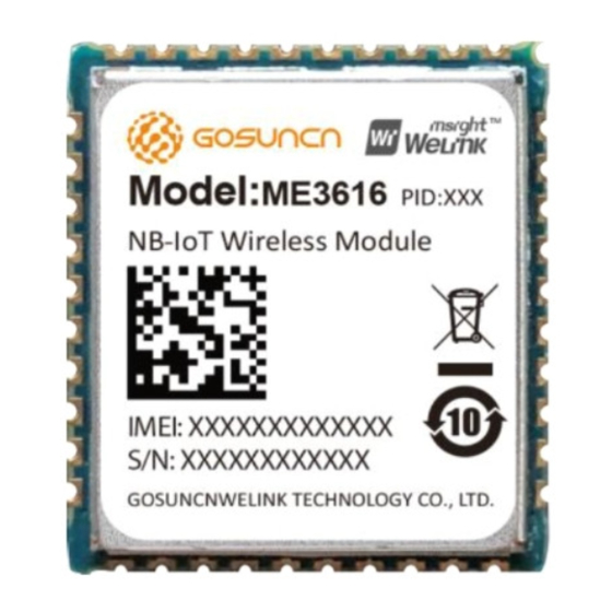
GOSUNCN WeLink ME3616 Manuals
Manuals and User Guides for GOSUNCN WeLink ME3616. We have
1
GOSUNCN WeLink ME3616 manual available for free PDF download: Hardware Development Manual
GOSUNCN WeLink ME3616 Hardware Development Manual (55 pages)
Brand:
GOSUNCN
| Category:
GSM/GPRS Modules
| Size: 3 MB
Table of Contents
Revision History
2
About this Document
2
Safety Information
4
Table of Contents
5
Tables
7
1 Product Overview
11
General Description
11
Key Features
11
Table 1-1 ME3616 Supported Band
11
Table 1-2 ME3616 Key Features
11
Function Diagram
12
Figure 1-1 System Connection Structure
12
2 Application Interface
13
General Description
13
Eneral Escription
13
Pin Assignment
13
Pin Description
13
Figure 2-1 Pin Assignment
13
Table 2-1 IO Parameters Definition
14
Table 2-2 Logic Levels Description
14
Table 2-3 Pin Description
14
Orking Mode
16
Power Supply
17
Power Supply Pins
17
Decrease Voltage Drop
17
Table 2-4 Power Supply
17
Figure 2-2 Working Mode Switch
17
Reference Circuit of Power Supply
18
Vcc1V8_Out Reference Design
18
Table 2-5 VCC1V8_OUT Pin Definication
18
Figure 2-3 the Input Reference Circuit of VBAT
18
Figure 2-4 Reference Circuit of DC-DC
18
Power on Scenario
19
Table 2-6 Definition of POWER_ON
19
Figure 2-5 VCC1V8_OUT Reference Design
19
Table 2-7 Power-On Time
21
Figure 2-6 Reference Circuit of POWER_ON
21
Figure 2-7 Timing of Turning on Module
21
Figure 2-8 Timing of Wakeup Module through Pin POWER_ON
21
Turn off Scenarios
22
Urn off Cenarios
22
Reset Scenario
22
Table 2-8 Power-Off Time
22
Figure 2-9 Timing of Turning off Mode
22
Table 2-9 Definition of RESET
23
Table 2-10 Resetting Timing
23
Figure 2-10 Reference Circuit to Reset Module
23
Usim Interface
24
Description of Pins
24
Figure 2-11 Timing of Reset Mode
24
Figure 2-12 Pin Definition of the USIM Interface
24
Design Considerations for USIM Card Holder
25
Figure 2-13 Reference Design of USIM Interface
25
Table 2-11 Pin Description of Molex USIM Card Holder
26
Figure 2-14 Molex 91228 USIM Card Holder
26
Table 2-12 Pin Description of Amphenol USIM Card Holder
27
Figure 2-15 Amphenol C707 10M006 512 2 USIM Card Holder
27
Uart Interface
28
UART Connection
28
Table 2-13 Pin Definition of the Main UART Interface
28
2.11.2. Uart Level Match
29
Figure 2-16 Schematic of 3-Wire UART Connection
29
Figure 2-17 Schematic of 4-Wire UART Connection
29
Figure 2-18 Recommended TXD Circuit
30
Figure 2-19 Recommended RXD Circuit
31
Figure 2-20 Recommended RTS Circuit
32
Use IC for Level Switch
33
Figure 2-21 Recommended CTS Circuit
33
Figure 2-22 Recommended 4-Wires UART Level Switch Circuit
34
Figure 2-23 Recommended 2-Wires UART Level Switch Circuit
34
Figure 2-24 Debug UART Interface Definication
34
Network Status Indicator
35
Etwork Tatus Ndicator
35
Table 2-14 Pin Definition of Network Indicator
35
Figure 2-25 the Test Point of Debug UART
35
Adc Interface
36
Gpio Interface
36
Table 2-15 Pin Definition of the ADC
36
Table 2-16 Characteristic of the ADC
36
Table 2-17 Pin Definition of GPIO
36
Figure 2-26 Connections of the SYS_STATE Pin
36
Ignal
37
Table 2-18 Pin Definition of WAKEUP_IN
37
Figure 2-27 WAKEUP_IN Input Sequence
37
Ignal
38
Table 2-19 Pin Definition of WAKEUP_OUT
38
Figure 2-28 Connections of the WAKEUP_IN Pin
38
Figure 2-29 WAKEUP_OUT Output Sequence
38
Figure 2-30 Connections of the WAKEUP_OUT Pin
38
Usb Interface
39
Figure 2-31 USB Interface Connection
39
3 Antenna Interface
40
Pin Definition
40
Reference Design
40
Reference Pcb Layout of Antenna
40
Table 3-1 Pin Definition of Antenna
40
Figure 3-1 Reference Circuit of Antenna Interface
40
Suggestions for Emc & Esd Design
41
EMC Design Requirements
41
ESD Design Requirements
41
Test Methods for Whole -Set Antenna Ota
41
Figure 3-2 the OTA Test System of CTIA
42
4 Electrical, Reliability and Radio Characteristics
43
Operating Temperature
43
Perating Emperature
43
Current Consumption
43
Rf Output Power
43
Table 4-1 Operating Temperature
43
Table 4-2 Average Current Consumption
43
Table 4-3 RF Output Power
43
Rf Receiving Ensitivity
44
Electrostatic Discharge
44
Table 4-4 RF Receiving Sensitivity
44
Table 4-5 ESD Characteristic
44
5 Mechanical Dimensions
45
Mechanical Dimensions of the Module
45
Figure 5-1 ME3616 Top Dimensions(Tolerance:±0.1Mm
45
Figure 5-2 ME3616 Bottom Dimensions (Perspective View)
46
Recommended Package Size
47
Figure 5-3 Recommended Package Size(Unit:MM
47
6 Related Test & Test Standard
48
Testing Reference
48
Description of Testing Environment
48
Table 6-1 Testing Standard
48
Reliability Testing Environment
49
Table 6-2 Testing Environment
49
Table 6-3 Testing Instrument & Device
49
Table 6-4 Reliability Features
49
7 Smt Process and Baking Guide
51
Storage Requirements
51
Odule Lainness Tandard
51
Rocess Outing Election
51
Solder Paste Selection
51
Design of Module Pad's Steel Mesh Opening on Main Board
51
Table 7-1 Baking Parameters
51
Module Board's SMT Process
52
Table 7-2 LCC Module Pad's Steel Mesh Opening
52
Figure 7-1 Module Board's Steel Mesh Diagram
52
Figure 7-2 Material Module Pallet
53
Figure 7-3 Tape Reel Dimension
53
Module Soldering Reflow Curve
54
Reflow Method
54
Maintenance of Defects
54
Figure 7-4 Module Furnace Temperature Curve Reference Diagram
54
Module ' S Baking Requirements
55
Module's Baking Environment
55
Baking Device and Operation Procedure
55
Module Baking Conditions
55
Advertisement
Advertisement
Related Products
GOSUNCN ME3630 Series
GOSUNCN ME3630-E
GOSUNCN ME3630-U
GOSUNCN ME3630-J
GOSUNCN ME3630-A
GOSUNCN ME3630 mini-PCIE
GOSUNCN Categories
Control Unit
GSM/GPRS Modules
Network Router
GPS
Microphone system
More GOSUNCN Manuals
Login
Sign In
OR
Sign in with Facebook
Sign in with Google
Upload manual
Upload from disk
Upload from URL