Sign In
Upload
Manuals
Brands
Geehy SEMICONDUCTOR Manuals
Microcontrollers
APM32F407 Series
Geehy SEMICONDUCTOR APM32F407 Series Manuals
Manuals and User Guides for Geehy SEMICONDUCTOR APM32F407 Series. We have
2
Geehy SEMICONDUCTOR APM32F407 Series manuals available for free PDF download: User Manual
Geehy SEMICONDUCTOR APM32F407 Series User Manual (662 pages)
Arm Cortex-M4 based 32-bit MCU
Brand:
Geehy SEMICONDUCTOR
| Category:
Microcontrollers
| Size: 12 MB
Table of Contents
Table of Contents
2
Document Description Rules
9
Introduction and Document Description Rules
9
Introduction
9
System Architecture Block Diagram
13
System Architecture
13
Full Name and Abbreviation Description of Terms
13
Memory Mapping
16
Startup Configuration
16
FLASH Memory
18
Full Name and Abbreviation Description of Terms
18
Introduction
18
Main Characteristics
18
Flash Memory Structure
19
Flash Memroy Functional Description
19
Register Address Mapping
26
Register Functional Description
26
SMC Introduction
31
Full Name and Abbreviation Description of Terms
31
External Memory Controller (EMMC)
31
EMMC Overview
31
SMC Structure Block Diagram
32
SMC Functional Description
32
SMC Register Address Mapping
38
SMC Register Functional Description
39
DMC Introduction
48
Main Characteristics of DMC
48
DMC Structure Block Diagram
49
DMC Functional Description
49
DMC Register Address Mapping
51
DMC Register Functional Description
51
Register Address Mapping
56
Register Functional Description
56
I/O Compensation Cell
56
Main Characteristics
56
System Configuration Controller (SYSCFG)
56
Reset Management Unit (RMU)
61
Reset and Clock (RCM)
61
Full Name and Abbreviation Description of Terms
61
Clock Management Unit (CMU)
64
Register Address Mapping
71
Register Functional Description
72
Power Management Unit (PMU)
102
Full Name and Abbreviation Description of Terms
102
Introduction
102
Structure Block Diagram
103
Functional Description
103
Register Address Mapping
110
Register Functional Description
110
Interrupt and Exception Vector Table
113
Main Characteristics
113
Introduction
113
Nested Vector Interrupt Controller (NVIC)
113
Full Name and Abbreviation Description of Terms
113
External Interrupt/Event Controller (EINT)
121
Introduction
121
Main Characteristics
121
Functional Description
121
Register Address Mapping
124
Register Functional Description
124
Direct Memory Access (DMA)
127
Introduction
127
Main Characteristics
127
Functional Description
127
DMA Register Address Mapping
134
Register Functional Description
134
Introduction
143
Main Characteristics
143
Full Name and Abbreviation Description of Terms
143
Debug MCU (DBGMCU)
143
Functional Description
144
Register Address Mapping
145
Register Functional Description
145
General-Purpose Input/Output Pin (GPIO)
150
Full Name and Abbreviation Description of Terms
150
Main Characteristics
150
Structure Block Diagram
151
Functional Description
151
Register Address Mapping
155
Register Functional Description
155
Timer Overview
160
Full Name and Abbreviation Description of Terms
160
Timer Category and Main Difference
160
Main Characteristics
163
Introduction
163
Advanced Timers (TMR1/8)
163
Structure Block Diagram
164
Functional Description
164
Register Address Mapping
181
Register Functional Description
182
Control Event Generation Register (Tmrx_Ceg)
189
General-Purpose Timer (TMR2/3/4/5)
201
Introduction
201
Main Characteristics
201
Functional Description
202
Structure Block Diagram
202
Register Address Mapping
215
Register Functional Description
215
Capture/Compare Channel3 Repetition Capture Flag Refer to STS_CC1RCFLG
222
Capture/Compare Channel4 Repetition Capture Flag Refer to STS_CC1RCFLG
222
Cc3Rcflg Rc_W0
222
Cc4Rcflg Rc_W0
222
Control Event Generation Register (Tmrx_Ceg)
222
Refer to STS_CC1RCFLG
222
General-Purpose Timer (TMR9/10/11/12/13/14)
232
Introduction
232
Main Characteristics of TMR10/11/13/14
232
Main Characteristics of TMR9/12
232
TMR9/12 Structure Block Diagram
233
Functional Description
234
TMR10/11/13/14 Structure Block Diagram
234
TMR9/12 Register Address Mapping
241
TMR9/12 Register Functional Description
242
State Register (Tmrx_Sts)
245
TMR10/11/13/14 Register Address Mapping
251
TMR10/11/13/14 Register Functional Description
252
0: Input Capture DID Not Occur
253
1: Input Capture Occurred
253
Capture/Compare Channel1 Interrupt Flag When the Capture/Compare Channel 1 Is Configured as Output: 0: no Matching Occurred 1: the Value of Tmrx_Cnt Matches the Value of Tmrx_Cc1
253
Cc1Iflg Rc_W0
253
Name R/W Description
253
Offset Address: 0X10 Reset Value: 0X0000
253
On Tmrx_Ceg Register to Generate Update Event, and the Counter Needs to be Initialized by Software
253
Repeat Counter Overruns/Underruns, an Update Event will be
253
State Register (Tmrx_Sts)
253
Uiflg Rc_W0
253
1: Repeat Capture Occurs
254
Capture/Compare Channel1 Repetition Capture Flag
254
Cc1Rcflg Rc_W0
254
Basic Timer (TMR6/7)
259
Functional Description
259
Introduction
259
Main Characteristics
259
Structure Block Diagram
259
Register Address Mapping
261
Register Functional Description
262
Independent Watchdog Timer (IWDT)
266
Introduction
266
Watchdog Timer (WDT)
266
Window Watchdog Timer (WWDT)
268
IWDT Register Address Mappin
269
IWDT Register Functional Description
270
WWDT Register Address Mappin
271
WWDT Register Functional Description
271
Full Name and Abbreviation Description of Terms
273
Introduction
273
Main Characteristics
273
Real-Time Clock (RTC)
273
Structure Block Diagram
273
Functional Description
274
Register Address Mapping
280
Register Functional Description
281
Functional Description
297
HASH Processor (HASH)
297
Introduction
297
Main Characteristics
297
Register Address Mapping
298
Register Functional Description
298
Digital Camera Interface (DCI)
303
Full Name and Abbreviation Description of Terms
303
Introduction
303
Main Characteristics
303
Functional Description
304
Structure Block Diagram
304
Register Address Mapping
308
Register Functional Description
309
Full Name and Abbreviation Description of Terms
315
Introduction
315
Main Characteristics
315
Universal Synchronous/Asynchronous Transceiver (USART)
315
Functional Description
317
Register Address Mapping
331
Register Functional Description
331
Full Name and Abbreviation Description of Terms
339
Internal Integrated Circuit Interface (I2C)
339
Introduction
339
Main Characteristics
339
Functional Description
341
Structure Block Diagram
341
Register Address Mapping
348
Register Functional Description
348
Full Name and Abbreviation Description of Terms
358
Introduction
358
Serial Peripheral Interface/On-Chip Audio Interface (SPI/I2S)
358
Main Characteristics
359
SPI Functional Description
360
I2S Functional Description
371
Register Address Mapping
383
Register Functional Description
384
Controller Area Network (CAN)
391
Full Name and Abbreviation Description of Terms
391
Functional Description
391
Introduction
391
Main Characteristics
391
Register Address Mapping
400
Register Functional Description
401
Full Name and Abbreviation Description of Terms
419
Functional Description
419
Introduction
419
Main Characteristics
419
Secure Digital Input/Output Interface (SDIO)
419
Register Address Mapping
442
Register Functional Description
442
Introduction
454
OTG_FS Global Register Address Mapping
454
Usb_Otg
454
OTG_FS Global Register Functional Description
455
OTG_FS Host Mode Register Address Mapping
469
OTG_FS Host Mode Register Functional Description
470
OTG_FS Device Mode Register Address Mapping
476
OTG_FS Device Mode Register Functional Description
477
Full-Speed OTG Power and Clock Gating Control Register (OTG_FS_PCGCTRL)
492
OTG_HS1 Global Register Address Mapping
493
OTG_HS1 Global Register Functional Description
494
OTG_HS1 Host Mode Register Address Mapping
511
OTG_HS1 Host Mode Register Functional Description
511
OTG_HS1 Device Mode Register Address Mapping
519
OTG_HS1 Device Mode Register Functional Description
520
(Otg_Hs1_Pcgctrl)
538
High-Speed OTG Power and Clock Gating Control Register
538
OTG_HS2 Global Register Functional Description
539
OTG_HS2 Register Address Mapping
539
Ethernet
541
Introduction
541
Main Characteristics of Ethernet
541
Functional Description
544
MAC Register Address Mapping
573
MAC Register Functional Description
574
MMC Register Address Mapping
590
MMC Register Functional Description
590
PTP Register Address Mapping
594
PTP Register Functional Description
594
DMA Register Address Mapping
599
DMA Register Functional Description
599
Analog-To-Digital Converter (ADC)
611
Full Name and Abbreviation Description of Terms
611
Introduction
612
Main Characteristics
612
Functional Description
613
Register Address Mapping
624
Register Functional Description
625
Digital-To-Analog Converter (DAC)
636
Full Name and Abbreviation Description of Terms
636
Functional Description
636
Introduction
636
Structure Block Diagram
636
Register Address Mapping
640
Register Functional Description
640
Functional Description
646
Introduction
646
Main Characteristics
646
Random Number Generator (RNG)
646
Register Address Mapping
647
Register Functional Description
647
Cryp
650
Interrupt
650
Introduction
650
Main Characteristics
650
Dma
651
Register Address Mapping
651
Register Functional Description
651
Cyclic Redundancy Check Computing Unit (CRC)
656
Functional Description
656
Introduction
656
Register Address Mapping
656
Register Functional Description
656
Chip Electronic Signature
658
Introduction
658
Register Functional Description
658
Version History
659
Advertisement
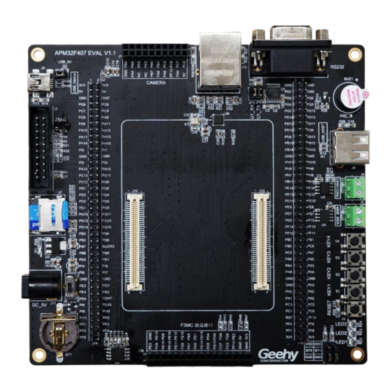
Geehy SEMICONDUCTOR APM32F407 Series User Manual (26 pages)
Brand:
Geehy SEMICONDUCTOR
| Category:
Motherboard
| Size: 1 MB
Advertisement
Related Products
Geehy SEMICONDUCTOR APM32F407/417 E G Series
Geehy SEMICONDUCTOR APM32F407IGT6
Geehy SEMICONDUCTOR APM32F407IET6
Geehy SEMICONDUCTOR APM32F407ZGT6
Geehy SEMICONDUCTOR APM32F407ZET6
Geehy SEMICONDUCTOR APM32F407VGT6
Geehy SEMICONDUCTOR APM32F407VET6
Geehy SEMICONDUCTOR APM32F407RGT6
Geehy SEMICONDUCTOR APM32F407RET6
Geehy SEMICONDUCTOR APM32F405/415 G Series
Geehy SEMICONDUCTOR Categories
Motherboard
Microcontrollers
More Geehy SEMICONDUCTOR Manuals
Login
Sign In
OR
Sign in with Facebook
Sign in with Google
Upload manual
Upload from disk
Upload from URL