Sign In
Upload
Manuals
Brands
ADLINK Technology Manuals
Computer Hardware
MCM-100
ADLINK Technology MCM-100 Manuals
Manuals and User Guides for ADLINK Technology MCM-100. We have
1
ADLINK Technology MCM-100 manual available for free PDF download: User Manual
ADLINK Technology MCM-100 User Manual (117 pages)
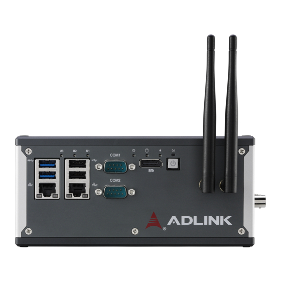
Edge IoT Platform for Machine Condition Monitoring
Brand:
ADLINK Technology
| Category:
Computer Hardware
| Size: 6 MB
Table of Contents
Table of Contents
7
List of Tables
13
List of Figures
15
Introduction
17
Features
17
Specifications
18
General
18
I/O
19
Power Consumption
22
Mechanical Drawings
24
Figure 1-1: Top View
24
Figure 1-2: Front View
24
Figure 1-3: MCM-100 (Right) Side View
25
Figure 1-4: MCM-102 (Right) Side View
25
I/O Connectors
26
Figure 1-5: (Left) Side View
26
Figure 1-6: Front Panel I/O
26
Figure 1-7: MCM-100 Right Side Panel I/O
27
Figure 1-8: MCM-102 Right Side Panel I/O
27
Power Button
28
Figure 1-9: Left Side Panel I/O
28
Reset Button
29
Displayport Connector
29
Table 1-1: Displayport Pin Assignment
29
LED Indicators
30
DB-9P COM Port Connector
30
Table 1-2: LED Operation Indicators
30
Table 1-3: DB-9P COM Port Pin Assignment
30
Figure 1-10: DB-9P COM Port
30
Dual Gigabit Ethernet Ports
31
USB 3.0 Port
32
BNC Connectors
32
Table 1-4: Gigabit Ethernet Port LED Function
32
Figure 1-11: BNC Connector Polarity
32
4-Pin GPI/O W/ DGND Connector
33
DC Power Supply Connector
33
Adapters and Other Accessories
33
Figure 1-12: 4-Pin GPI/O W/ DGND Connector
33
Figure 1-13: DC Power Connector
33
Getting Started
35
Unpacking Checklist
35
Connecting DC Power
35
DIN Rail Mounting
35
Wall Mounting
38
Cooling Considerations
39
Installing Mini-Pcie Wifi Module (Optional)
40
Driver & Application Installation
45
Installing the Chipset Driver
45
Installing the Graphics Driver
46
Installing the Ethernet Driver
46
Installing the USB 3.0 Driver
47
Installing the I/O Controller Driver
47
Installing the SEMA Utility, WDT and DI/O Drivers
47
Installing AI and DI/O Drivers
48
MAPS Core
48
DAQ-LVIEW Plus
49
Operation
51
Analog Input
51
Analog Input Front End Configuration
51
Input Configuration: Differential/Pseudo-Differential
51
Table 4-1: Signal Source-Card Configuration
51
Figure 4-1: MCM-100/102 Analog Front End
51
Input Coupling
52
IEPE Input
52
Figure 4-2: Excitation Current for IEPE Sensor Measurement
52
AI Data Format
53
Sampling Rate
53
DDS Timing/Sampling Rate
53
Table 4-2: MCM-100/102 Input Ranges
53
Data Transfer
54
Software Polling Data Transfer (Non-Buffering Programmed I/O)
54
Continuous Acquisition Mode
54
Anti-Aliasing Filter and Frequency Response
54
Figure 4-3: Input Frequency Response for High Resolution Mode
55
Triggering
56
Analog Input Trigger Source
56
Software Triggering
56
Figure 4-4: Input Frequency Response for High Speed Mode
56
External Analog Trigger
57
Figure 4-5: Below-Low Analog Triggering
57
External Digital Triggering
58
Figure 4-6: Above-High Analog Triggering
58
Figure 4-7: Digital Triggering
58
Trigger Modes
59
Figure 4-8: Post Trigger Without Retrigger
59
Delay-Trigger Acquisition (no Retrigger)
60
Figure 4-9: Pre-Trigger Mode Operation (Valid Trigger Only)
60
Figure 4-10: Pre-Trigger Mode Operation (W/ Invalid Trigger)
60
Middle-Trigger Acquisition
61
Gated Trigger
61
Figure 4-11: Delay-Trigger Mode Operation
61
Figure 4-12: Middle-Trigger Acquisition
61
Post-Trigger or Delay-Trigger Acquisition with Re-Trigger
62
Programmable Function I/O
62
Static Digital Input/Output
62
Frequency Counter
62
Figure 4-13: Gated Trigger
62
Pulse Output
63
Digital Trigger in for Continuous Analog Input
63
Synchronization Sample Clock in
63
Calibration
65
Loading Calibration Constants
65
Auto-Calibration
65
Saving Calibration Constants
66
A Appendix: BIOS Setup
67
Main
68
BIOS Information
68
System Time/System Date
68
Board Information
69
Advanced
70
CPU Configuration
71
Active Processor Cores
71
Intel Virtualization Technology
71
VT-D
71
Turbo Mode
71
Critical Trip Point
72
Passive Cooling Trip Point
72
Graphics Configuration
72
GTT Size
72
Aperture Size
72
DVMT Pre-Allocated
73
DVMT Total Gfx Mem
73
Onboard Device Configuration
73
COM1 Control
73
COM2 Control
73
Hsuart
74
LAN #1 (Intel I210)
74
LAN #2 (Intel I210)
74
Realtek Audio Support
74
Console Redirection
75
Console Redirection Settings (COM 1)
75
Console Redirection
78
Console Redirection Settings (COM 2)
78
Advanced Power Management
80
Power Supply Unit
81
State after G3
81
RTC Wake System from S5
81
LAN #1 Wake
81
LAN #2 Wake
81
USB Configuration
82
XHCI Hand-Off
82
USB Mass Storage Driver Support
82
USB Transfer Time-Out
82
Device Reset Time-Out
82
Device Power-Up Delay
83
SATA Configuration
83
Port
83
TPM Configuration
84
Security Device Support
84
Network Stack Configuration
85
Network Stack
85
System Management
86
Flags
90
Power up
91
Miscellaneous
92
OS Selection
92
Intel® I210 Gigabit Network Connection
93
Blink Leds
93
NIC Configuration
94
Link Speed
94
Wake on LAN
94
Security
95
Administrator Password
95
User Password
95
BIOS Lock
95
Secure Boot
96
Boot
97
Setup Prompt Timeout
97
Bootup Numlock State
97
Quiet Boot
97
Fast Boot
97
Boot Option Priorities
98
Save & Exit
98
Save Changes and Exit
98
Discard Changes and Exit
98
Save Changes and Reset
99
Discard Changes and Reset
99
Save Changes
99
Discard Changes
99
Restore Defaults
99
Save as User Defaults
99
Restore User Defaults
99
Launch EFI Shell from Filesystem Device
99
B Appendix: Functional Information
101
Figure B-1: MCM-100/102 System Functional Block Diagram
101
AI and GPI/O Functional Layout
102
Figure B-2: MCM-100/102 AI and GPI/O Functional Block Diagram
102
Internal I/O Connectors
103
Figure B-3: Mainboard Top View
103
Figure B-4: Mainboard Underside View
104
Internal HSUART Interface Wafer
105
USIM Port
105
Table B-1: Internal I/O Legend
105
Table B-2: HSUART Interface Wafer Pin Definitions
105
Internal USB2.0 Interface Wafer
106
Internal I2C Interface Wafer
106
Table B-3: USB2.0 Interface Wafer Pin Definitions
106
Clear CMOS Jumper
107
GPS Antenna Power Header
107
Table B-4: Internal I2C Interface Wafer Pin Definitions
107
Table B-5: Clear CMOS Jumper Pin Definition
107
Internal SATA Interface Wafer
108
Table B-6: +5V GPS Antenna Power Connector Pin Definition
108
Table B-7: SATA Wafer Pin Definition
108
Extended Power Wafer
109
Table B-8: Extended Power Header Connector Pin Definition
109
Internal I2C Interface Wafer
110
Extended Reset Wafer
110
Table B-9: I2C Box Header Connector Pin Definition
110
Table B-10: Extended Reset Header Connector Pin Definition
110
RTC Battery Header
111
Internal Speaker Wafer (Optional)
111
Table B-11: RTC Battery Connector Pin Definition
111
Table B-12: Speaker Wafer Pin Definition
111
Internal MIC-IN & HP-OUT Wafer (Optional)
112
Table B-13: MIC-IN & HP-OUT Wafer Pin Definition
112
Important Safety Instructions
113
Getting Service
117
Advertisement
Advertisement
Related Products
ADLINK Technology MCM-102
ADLINK Technology MCM-216
ADLINK Technology MCM-218
ADLINK Technology MXE-5401
ADLINK Technology MXM-P1000
ADLINK Technology MXM-AXe
ADLINK Technology Matrix MXE-3000 Series
ADLINK Technology Matrix MXE-3002
ADLINK Technology MEC-AI7400SR
ADLINK Technology MCM-204
ADLINK Technology Categories
Computer Hardware
Motherboard
PCI Card
Control Unit
Desktop
More ADLINK Technology Manuals
Login
Sign In
OR
Sign in with Facebook
Sign in with Google
Upload manual
Upload from disk
Upload from URL