Sign In
Upload
Manuals
Brands
ADLINK Technology Manuals
Computer Hardware
DAQ-2213
ADLINK Technology DAQ-2213 Manuals
Manuals and User Guides for ADLINK Technology DAQ-2213. We have
1
ADLINK Technology DAQ-2213 manual available for free PDF download: User Manual
ADLINK Technology DAQ-2213 User Manual (97 pages)
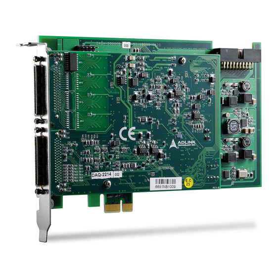
16-ch High Performance Low-Cost Data Acquisition Card
Brand:
ADLINK Technology
| Category:
Computer Hardware
| Size: 4 MB
Table of Contents
Revision History
3
California Proposition 65 Warning
5
Table of Contents
6
List of Tables
8
List of Figures
10
Introduction
12
Features
13
Applications
14
Specifications
14
Table 1-1: Programmabel Input Range
14
Table 1-2: Bandwidth
15
Table 1-3: System Noise
15
Table 1-4: CMRR (DC to 60 Hz)
16
Table 1-5: Settling Time to Full Scale Step
16
Software Support
20
Installation
24
Contents of Package
24
Unpacking
25
Daq/Daqe-2213/2214 Layout
26
Figure 2-1: PCB Layout of Daq/Daqe-2213/2214
26
Switch and Jumper Settings
27
Figure 2-2: Board ID SW1 DIP Switch
27
Table 2-1: Board ID SW1 DIP Switch Settings
28
Figure 2-3: Enable Board ID Configuration
29
Figure 2-4: DIO Initial Status (JP4)
30
PCI Configuration
31
Plug and Play
31
Troubleshooting
31
Signal Connections
32
Connector Pin Assignment
32
Table 3-1: CN1 Pin Assignment for Daq/Daqe-2213/2214
33
Table 3-2: CN2 Pin Assignment for Daq/Daqe-2213
34
Table 3-3: CN2 Pin Assignment for Daq/Daqe-2214
35
Table 3-4: CN1/CN2 Signal Description
36
Table 3-5: SSI Connector Pin Assignment for Daq/Daqe-2213
37
Table 3-6: SSI Connector Pin Assignment for Daq/Daqe-2214
37
Table 3-7: SSI Connector Legend
38
Analog Input Signal Connection
39
Figure 3-1: Floating Source and RSE Input Connections
40
Figure 3-2: Ground-Referenced Sources and NRSE Input
40
Figure 3-3: Ground-Referenced Source and Differential Input
41
Figure 3-4: Floating Source and Differential Input
41
Operation Theory
42
A/D Conversion
42
Table 4-1: Bipolar Analog Input Range and Output Digital Code
43
Table 4-2: Unipolar Analog Input Range and Output Digital Code
43
Programmable Scan Acquisition Mode
45
Figure 4-1: Scan Timing
46
Specifying Channels, Gains, and Input Configurations in the Channel Gain Queue
47
Trigger Modes
48
Pre-Trigger Acquisition
48
Figure 4-2: Pre-Trigger (Trigger Occurs after M Scans)
48
Figure 4-3: Pre-Trigger (Trigger with Scan in Progress)
49
Figure 4-4: Pre-Trigger with M_Enable=0 (Trigger Occurs before M Scans)
50
Figure 4-5: Pre-Trigger with M_Enable=1
51
Figure 4-6: Middle-Trigger with M_Enable = 1
52
Figure 4-7: Middle-Trigger (Trigger Occurs When a Scan Is in Progress)
53
Figure 4-8: Post-Trigger
54
Figure 4-9: Delay Trigger
55
Figure 4-10: Post Trigger with Re-Trigger
56
Figure 4-11: Linked List of PCI Address DMA Descriptors
58
D/A Conversion (for Daq/Daqe-2214 Only)
59
Table 4-3: Bipolar Output Code Table (Vref=10V if Internal Reference Is Selected)
59
Table 4-4: Unipolar Output Code Table (Vref=10V if Internal Reference Is Selected)
60
Software Update
60
Figure 4-12: Typical D/A Timing of Waveform Generation
62
Figure 4-13: Post Trigger Waveform Generation
63
Figure 4-14: Delay Trigger Waveform Generation
64
Figure 4-15: Re-Triggered Waveform Generation with Post-Trigger (Dly2_Counter=0)
64
Figure 4-16: Finite Iterative Waveform Generation with Post-Trigger (Dly2_Counter = 0)
65
Figure 4-17: Infinite Iterative Waveform Generation with Post-Trigger (Dly2_Counter = 0)
66
Figure 4-18: Stop Mode I
67
Figure 4-19: Stop Mode II
68
Figure 4-20: Stop Mode III
68
Digital I/O
69
General Purpose Timer/Counter Operation
70
General Purpose Timer/Counter Modes
71
Figure 4-21: Mode 1 Operation
71
Figure 4-22: Mode 2 Operation
72
Figure 4-23: Mode 3 Operation
73
Figure 4-24: Mode 4 Operation
74
Figure 4-25: Mode 5 Operation
75
Figure 4-26: Mode 6 Operation
76
Figure 4-27: Mode 7 Operation
77
Figure 4-28: Mode 8 Operation
77
Trigger Sources
78
Software-Trigger
78
External Analog Trigger
78
Table 4-5: Analog Trigger SRC1 (EXTATRIG) Ideal Transfer
79
Figure 4-29: Analog Trigger Block Diagram
79
Figure 4-30: Below-Low Analog Trigger Condition
80
Figure 4-31: Above-High Analog Trigger Condition
80
Figure 4-32: Inside-Region Analog Trigger Condition
81
Figure 4-33: High-Hysteresis Analog Trigger Condition
82
Figure 4-34: Low-Hysteresis Analog Trigger Condition
83
Figure 4-35: External Digital Trigger
83
User-Controllable Timing Signals
84
Figure 4-36: DAQ Signals Routing
84
Table 4-6: User-Controllable Timing Signals and Functionalities
85
Table 4-7: Auxiliary Function Input Signals and Functionalities
87
System Synchronization Interface
89
Table 4-8: SSI Timing Signal and Functions
89
Calibration
92
Loading Calibration Constants
92
Auto-Calibration
93
Saving Calibration Constants
93
Important Safety Instructions
94
Getting Service
96
Advertisement
Advertisement
Related Products
ADLINK Technology NuDAQ DAQ-2500 Series
ADLINK Technology DAQ-2214
ADLINK Technology DAQe-2213
ADLINK Technology DAQe-2214
ADLINK Technology DLAP-301 Series
ADLINK Technology DLAP-301-JNX
ADLINK Technology DLAP-301-Nano
ADLINK Technology DLAP-211-NanoO
ADLINK Technology DLAP-211-Orin Series
ADLINK Technology DLAP-211-Orin NX 8GB
ADLINK Technology Categories
Computer Hardware
Motherboard
PCI Card
Control Unit
Desktop
More ADLINK Technology Manuals
Login
Sign In
OR
Sign in with Facebook
Sign in with Google
Upload manual
Upload from disk
Upload from URL