Table of Contents
Advertisement
Quick Links
Download this manual
See also:
Owner's Manual
QQ
3 7 63 1515 0
TE
L 13942296513
www
.
011441
PA
19990210-140000
http://www.xiaoyu163.com
x
ao
u163
y
i
http://www.xiaoyu163.com
2 9
8
POWER AMPLIFIER
XH150
SERVICE MANUAL
Q Q
3
6 7
1 3
1 5
CONTENTS
SPECIFICATIONS ................................................... 3/4
PANEL LAYOUT ......................................................
DIMENSIONS ......................................................... 6
BLOCK DIAGRAM ................................................... 6
CIRCUIT BOARD LAYOUT & WRING ........................
DISASSEMBLY PROCEDURE .................................... 8
IC BLOCK DIAGRAM ................................................ 12
CIRCUIT BOARDS ................................................... 13
INSPECTIONS ................................................... 15/17
co
PARTS LIST
.
1.97K-9636
9 4
2 8
0 5
8
2 9
9 4
2 8
m
1.92K-173
Printed in Japan '99.2
9 9
9 9
5
7
Advertisement
Table of Contents

Related Manuals for Yamaha XH150


Summary of Contents for Yamaha XH150
- Page 1 3 7 63 1515 0 POWER AMPLIFIER XH150 SERVICE MANUAL L 13942296513 CONTENTS SPECIFICATIONS …………………………………………… 3/4 PANEL LAYOUT ……………………………………………… DIMENSIONS ………………………………………………… 6 BLOCK DIAGRAM …………………………………………… 6 CIRCUIT BOARD LAYOUT & WRING …………………… DISASSEMBLY PROCEDURE ……………………………… 8 IC BLOCK DIAGRAM ………………………………………… 12 CIRCUIT BOARDS ……………………………………………...
-
Page 2: Important Notice
IMPORTANT NOTICE This manual has been provided for the use of authorized Yamaha Retailers and their service personnel. It has been assumed that basic service procedures inherent to the industry, and more specifically Yamaha Products, are already known and understood by the users, and have therefore not been restated. -
Page 3: Specifications
XH150 3 7 63 1515 0 SPECIFICATIONS •General Specifications 150 W+150 W Power Output Level RL= 64 ohm (100 V) 20 Hz-20 kHz THD+N= 0.1 % RL= 32 ohm (70 V) Power Bandwidth Halfpower 10 Hz- 40 kHz (THD + N= 0.1 %) 0.1 %... - Page 4 XH150 3 7 63 1515 0 L 13942296513 u163 http://www.xiaoyu163.com...
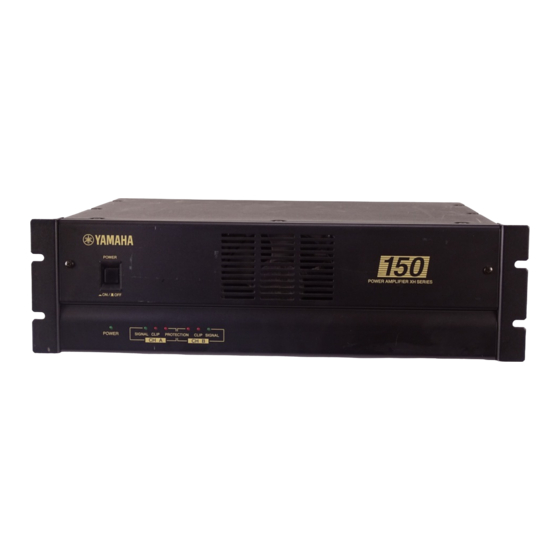
- Page 5 XH150 3 7 63 1515 0 PANEL LAYOUT Front Panel POWER POWER SIGNAL CLIP PROTECTION CLIP SIGNAL CH A CH B 1 POWER switch and indicator 2 SIGNAL indicators 3 CLIP indicators 4 PROTECTION indicator Rear Panel L 13942296513...
-
Page 6: Te L 13942296513
XH150 3 7 63 1515 0 DIMENSIONS L 13942296513 Unit: mm BLOCK DIAGRAM IC101 IC102 IC104 IC105 IC101 IC103 IC104 IC105 u163 KEC-92353 http://www.xiaoyu163.com... -
Page 7: Te L 13942296513
XH150 3 7 63 1515 0 CIRCUIT BOARD LAYOUT & WIRING Top View SUB 2/5 SUB 5/5 Power Transformer SUB 1/5 L 13942296513 SUB 4/5 Front View SUB 3/5 SUB 4/5 Wire color u163 3NC2-V294100 http://www.xiaoyu163.com... -
Page 8: Te L 13942296513
XH150 3 7 63 1515 0 DISASSEMBLY PROCEDURE Top Cover 1-1 Remove the nine (9) screws marked [410]. The top cover can then be removed. (Fig. 1, 2) Power Transformer 2-1 Remove the top cover. (See Procedure 1) 2-2 Remove the four (4) screws marked [70]. The power transformer can then be removed. -
Page 9: Te L 13942296513
XH150 3 7 63 1515 0 Panel Assembly 5-1 Remove the top cover. (See Procedure 1) 5-2 Remove the three (3) screws marked [380a] and the two (2) screws marked [380b]. The panel assembly can then be removed. (Fig. 3) SUB 3/5 Circuit Board 6-1 Remove the top cover. -
Page 10: Te L 13942296513
XH150 3 7 63 1515 0 10. PA7 Circuit Board 10-1 Remove the top cover. (See Procedure 1) 10-2 Remove the panel assembly. (See Procedure 5) 10-3 Remove the PA7 unit. (See Procedure 9) 10-4 Remove the sixteen (16) screws marked [80b]; the four (4) screws marked [80c] and the six (6) screws marked [60a]. - Page 11 XH150 3 7 63 1515 0 12. SUB 5/5 Circuit Board 12-1 Remove the top cover. (See Procedure 1) 12-2 Remove the rear assembly. (See Procedure 11) 12-3 Remove the two (2) screws marked [440] and the two (2) screws marked [420] and the two (2) screws marked [260b].
-
Page 12: Te L 13942296513
XH150 3 7 63 1515 0 IC BLOCK DIAGRAM M5238AP (XM085A00) Operational Amplifier IC101 +DC Voltage Output A Supply Inverting Output B Input A Non-Inverting Inverting Input A Input B Non-Inverting -DC Voltage Supply Input B L 13942296513 u163... - Page 13 http://www.xiaoyu163.com XS250/350 XS250/350 XS250/350 3 7 6 3 1 5 1 5 0 CIRCUIT BOARDS SUB 1/5 Circuit Board SUB 3/5 Circuit Board to PA7-CN404 Components side SUB 4/5 Circuit Board Components side from T101 SUB 2/5-CN103 PA7-CN702 from T101 1 3 9 4 2 2 9 6 5 1 3 SUB 2/5 Circuit Board Components side...
- Page 14 http://www.xiaoyu163.com XS250/350 XS250/350 XS250/350 3 7 6 3 1 5 1 5 0 PA7 Circuit Board to SUB 5/5-CN603 to SUB 2/5-CN101 SUB 2/5-CN102 1 3 9 4 2 2 9 6 5 1 3 from FAN to SUB7-CN509 Components side to SUB 3/5-CN401 w w w u 1 6 3...
- Page 15 XH150 3 7 63 1515 0 INSPECTIONS A STEREO and PARALLEL Operation Before performing any of the following adjustments, set the unit as follows: 1. ATTENUATIONS Maximum 2. Input terminal: Cannon connector pin 2 is HOT, pins 1 and 3 are GROUND 3.
- Page 16 XH150 3 7 63 1515 0 8. Channel Separation Test 8-1 Apply a - 5 dBu, 20kHz sine wave into the channel A input. 8-2 Short the input to channel B with a 600 ohm load. 8-3 Set the output of channel A at a reference of 0 dB.
-
Page 17: Http://Www.xiaoyu163.Com
XH150 3 7 63 1515 0 POWER AMPLIFIER XH150 PARTS LIST L 13942296513 CONTENTS OVERALL ASSEMBLY ............. 2 PA UNIT ..................4 ELECTRICAL PARTS ............... 5 Notes: DESTINATION ABBREVIATIONS A : Australian model : Japanese model B : British model U : U.S. - Page 18 XH150 3 7 63 1515 0 OVERALL ASSEMBLY UL only 260f 260i 260h 260g 260i 260i 260a 260e 260c L 13942296513 260d 260b u163 http://www.xiaoyu163.com...
-
Page 19: Circuit Boards
XH150 XH150 3 7 6 3 1 5 1 5 0 部 品 名 部 品 名 REF NO. PART NO. DESCRIPTION REMARKS QTY RANK REF NO. PART NO. DESCRIPTION REMARKS QTY RANK Overall Assembly XH150 総 組 立... - Page 20 XH150 XH150 3 7 6 3 1 5 1 5 0 PA UNIT REF NO. PART NO. DESCRIPTION 部 品 名 REMARKS QTY RANK PA Unit PAユニット PA 7 PAユニット V 2 9 4 1 7 0 0 PA Unit...
- Page 21 XH150 3 7 63 1515 0 ELECTRICAL PARTS REF NO. PART NO. DESCRIPTION REMARKS QTY RANK ELECTRCAL PARTS XH150 V 2 8 9 9 7 0 0 Circuit Board (XV024B0) AAX00030 Circuit Board SUB7 1/5 (XV420C0) AAX00040 Circuit Board...
- Page 22 XH150 3 7 63 1515 0 REF NO. PART NO. DESCRIPTION REMARKS QTY RANK D205 I F 0 0 5 5 6 0 Diode 1SS82TD D206 I F 0 0 5 5 6 0 Diode 1SS82TD D207 V D 6 3 1 6 0 0...
- Page 23 XH150 3 7 63 1515 0 REF NO. PART NO. DESCRIPTION REMARKS QTY RANK Q236 V 2 7 9 7 7 0 0 Transistor 2SC5395 E,F Q237 V 2 7 9 7 6 0 0 Transistor 2SA1993 E,F Q238...
-
Page 24: Http://Www.xiaoyu163.Com
XH150 3 7 63 1515 0 REF NO. PART NO. DESCRIPTION REMARKS QTY RANK R232 V V 0 6 6 0 0 0 Metal Film Resistor 33K 1/4F R233 H F 4 5 7 8 2 0 Carbon Resistor 82.0K 1/4 J... - Page 25 XH150 3 7 63 1515 0 REF NO. PART NO. DESCRIPTION REMARKS QTY RANK R313 H F 4 5 5 3 3 0 Carbon Resistor 330.0 1/4 J R314 H F 8 5 7 4 7 0 Carbon Resistor 47.0K 1/4 J...
- Page 26 XH150 3 7 63 1515 0 REF NO. PART NO. DESCRIPTION REMARKS QTY RANK R390 V Z 0 0 8 8 0 0 Flame Proof C. Resistor 22.0 1/4 J R391 V Z 3 7 0 1 0 0 Wire Wound Resistor 0.47 5W K...
- Page 27 XH150 3 7 63 1515 0 REF NO. PART NO. DESCRIPTION REMARKS QTY RANK C114 V V 0 6 2 4 0 0 Mylar Capacitor 0.047 50V J C115 V V 0 6 1 8 0 0 Mylar Capacitor 0.015 50V J...
- Page 28 XH150 3 7 63 1515 0 REF NO. PART NO. DESCRIPTION REMARKS QTY RANK Q409 V D 6 7 8 5 0 0 Digital Transistor DTA114ES Q501 V 2 7 9 7 6 0 0 Transistor 2SA1993 E,F Q502...
- Page 29 XH150 3 7 63 1515 0 REF NO. PART NO. DESCRIPTION REMARKS QTY RANK R602 V 2 9 6 1 0 0 0 Metal Oxide Film Resistor 4.7 2W J R603 V V 2 7 6 7 0 0 Flame Proof C.
- Page 30 XH150 XH150 OVERALL CIRCUIT DIAGRAM (PA7, SUB1/5 - SUB5/5) •NJM7815FA (XD853A00) •NJM7915FA (XD854A00) SUB2/5 SUB3/5 •REGULATOR •REGULATOR Capactor Mylar Capactor OP AMP Mylar Capactor Ceramic Capactor : Mica Capactor OP AMP OP AMP Resistor Flame Proot C. Resistor OP AMP OP AMP 1.OUTPUT...
Need help?
Do you have a question about the XH150 and is the answer not in the manual?
Questions and answers