Philips LX8200SA Service Manual
Av system
Hide thumbs
Also See for LX8200SA:
- Quick use manual (2 pages) ,
- Specifications (2 pages) ,
- Brochure & specs (2 pages)
Table of Contents
Advertisement
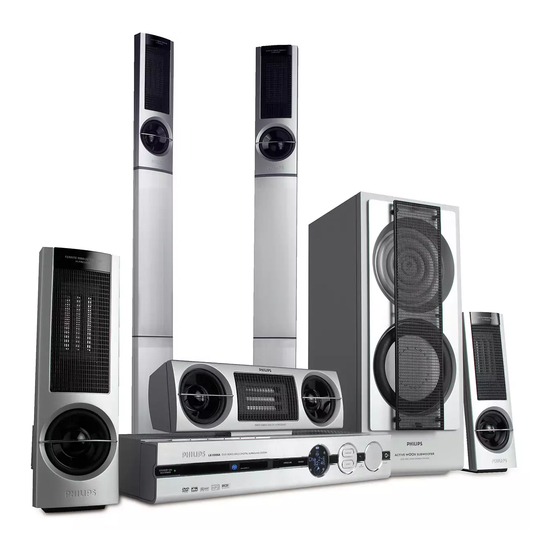
AV System
Service
Service
Service
Service
Service
1. For repair information on the SD4.00SA DVD Module, refer to Service Manual
"DVD Module SD-4.00SA_CH - 3122 785 12480".
2. For repair information on the Subwoofer SW8000SA/00S, refer to Service
Manual "SW8000SA/00S/01S/17S - 3139 785 30099".
Service Manual
©
Copyright 2003 Philips Consumer Electronics B.V. Eindhoven, The Netherlands
All rights reserved. No part of this publication may be reproduced, stored in a retrieval system or
transmitted, in any form or by any means, electronic, mechanical, photocopying, or otherwise
without the prior permission of Philips.
Published by BB 0316 Service Audio
Version 1.1
TABLE OF CONTENTS
Location of pc boards & Version variations ................ 1-2
Technical Specifications ............................................. 1-3
Measurement setup .................................................... 1-4
Service Aids, Safety Instruction, etc. .......................... 1-5
Reprogramming of DVD version matrix ..................... 1-7
Setting the TV system default .................................... 1-8
Disassembly Instructions & Service positions .............. 2
Service Test Programs .................................................. 3
Set Block diagram ...................................................... 4-1
Set Wiring diagram ..................................................... 5-1
Key & Control Boards .................................................... 6
ECO6 Tuner Board : Systems Cenelec ..................... 7B
Supply & Main Boards ................................................... 8
Power Amplifier Board ................................................... 9
AVC Board ................................................................... 10
P-Scan Board .............................................................. 11
Set Mechanical Exploded view & parts list ................. 12
Revision List ................................................................ 13
Printed in The Netherlands
Subject to modification
LX8200SA/
Page
CLASS 1
LASER PRODUCT
GB
22S
COMPACT
DIGITAL AUDIO
3139 785 30361
Advertisement
Table of Contents

Subscribe to Our Youtube Channel
Related Manuals for Philips LX8200SA


Summary of Contents for Philips LX8200SA
- Page 1 LASER PRODUCT © Copyright 2003 Philips Consumer Electronics B.V. Eindhoven, The Netherlands All rights reserved. No part of this publication may be reproduced, stored in a retrieval system or transmitted, in any form or by any means, electronic, mechanical, photocopying, or otherwise without the prior permission of Philips.
- Page 2 SPECIFICATIONS GENERAL: AUDIO INPUTS / OUTPUTS: Input sensitivity Mains voltage : 110-127V/220-240V Switchable for /21 : 880mV ± 3dB 120V for /37 Aux in (at 1kHz) : 350mV ± 3dB TV in (at 1kHz) 220-230V for /22 Mains frequency : 50/60Hz Power consumption : <...
- Page 3 - <Cursor Down> key 4 times - <Cursor Right> key 1 time - <Cursor Down> key 4 times 3) Message "(C)PHILIPS 01- 02 5580 W.WW.WW ..PXXXXXXXX Y.YY.Y" will be displayed on the TV screen: W.WW.WW - indicate the BEA software version number PXXXXXXXX - indicate the version matrix programmed Y.YY.Y...
- Page 4 Setting the TV system default 1) Press <SYSTEM MENU> on the Remote Control to enter the User Preference Manual (UPM). 2) From the User Preference Manual on the TV screen, select TV SYSTEM to change the TV system default accordingly as shown in the table below: Version Region TV system default...
- Page 5 DISMANTLING INSTRUCTIONS Dismantling of the Tuner Board and Main Board and AVC Board Dismantling of the Tuner Board and Main Board and AVC Board 1) Loosen 6 screws A to remove the Cover Top (pos 260). 2) Remove 3 screws B and uncatch 2 catches B1 (see Figure 3) Remove the Bracket PCB Mains (pos 259) by pressing 4) Remove 1 screw C (see Figure 2) and uncatch 2 catches - 2 screws each on the left &...
- Page 6 DISMANTLING INSTRUCTIONS Dismantling of the Supply Board and Power Amplifier Board Dismantling of the DVD Module 1) Remove 7 screws D to loosen the Supply Board (pos 1) Use a Flat Head screw driver to give a push in the 1104-A) and Power Amplifier Board (pos 1103).
- Page 7 DISMANTLING INSTRUCTIONS Dismantling of the Front Panel Assembly Dismantling of the Key & Control Boards 1) Remove 7 screws H (see Figure 12 and Figure 13) and 2) Make sure to unplug the cable (if obstructed) before 1) Remove 1 screw K (see Figure 15) to loosen the 4) Remove 2 screws N (see Figure 16) to loosen the uncatch 2 catches H1 (see Figure 13) to loosen the Front separate the Front Panel Assembly from the set (see...
- Page 8 DISMANTLING INSTRUCTIONS Service position A Service position D Use a insulation sheet to prevent any damaged or short-circuit of the boards. Service position B Service position E Use a insulation sheet to prevent any damaged or short-circuit of the boards. Service position F Service position C...
-
Page 9: Service Test Programs
SERVICE TEST PROGRAM To start service test program hold T & SOURCE depressed while plugging in the mains cord S refers to Service Mode Display shows the ROM version V refers to Version "S-Vyy" (Main menu) yy refers to Software version number of the uProcessor (counting up from 01 to 99) QUARTZ DISPLAY... - Page 10 SERVICE TEST PROGRAM To start service test program hold T & SOURCE depressed while plugging in the mains cord S refers to Service Mode Display shows the ROM version V refers to Version "S-Vyy" (Main menu) yy refers to Software version number of the uProcessor (counting up from 01 to 99) DVD SERVICE TEST...
- Page 11 SET BLOCK DIAGRAM HEF4053BT FM-95.00 POWER AMP DIG_IN_CTRL BC369 & LD1117 BC369 UDA1351TS L3-BUS INTERFACE DIG_IN_CTRL SURROUND POWER AMP IEC958 DECODER CLK & TIMING CIRCUIT CENTRE POWER AMP MUTE_DVD FLI2200 MAINS TRAFO ADV7300 PLL / CLK SYNC GENERATOR GENERATOR INPUT LPS COIL OUTPUT SIGNAL...
- Page 12 SET WIRING DIAGRAM 0385 TRAFO 340mm side 180mm 180mm 340mm MAIN 4P 140mm BD side AMPLIFIER 13P 340mm AD FOLD 7P 140mm BD 1580 5P 140mm BD SACD 180mm side 280mm 1615 6P 120mm 120mm FOLD side side SUPPLY VOLUME / IR 14P 120mm AD FOLD 1581 side...
-
Page 13: Key & Control Boards
LCD MODULE BLOCK DIAGRAM LCD PANEL 48 * 15 DOTS with 38 ICONS KEY & CONTROL BOARDS IC AX6120 TABLE OF CONTENTS LCD Module - Block diagram .......... 6-1 INTERFACE LCD Module - Interface Pin Function ......6-1 Top Key Part - Layout & Circuit diagram ......6-2 SACD LED Part - Layout &... - Page 14 TOP KEY BOARD - COMPONENT LAYOUT TOP KEY BOARD - CIRCUIT DIAGRAM 1310 A3 1313 D3 1335 A2 2301 A1 3302 B2 3305 C2 3308 E2 1311 B3 1314 E3 1801 A1 3300 B2 3303 C2 3306 D2 3309 E2 1312 C3 1315 E2 2300 A1...
- Page 15 SACD LED BOARD - COMPONENT LAYOUT SACD LED BOARD - CIRCUIT DIAGRAM 1580 A1 1581 B3 3530 B2 3531 C2 3532 C2 6580 B2 7580 C2 This assembly drawing shows a summary of all possible versions. For components used in a specific version see schematic diagram and respective parts list. SACD LED FE-ST-VK-N 1580...
- Page 16 VOLUME & IR BOARD - CIRCUIT DIAGRAM 1235 A1 1236 A3 1237 C4 1242 C6 1243 C7 1244 D3 1245 C7 1246 C8 2211 D4 2212 D4 2214 B7 2215 A7 2216 A6 2217 C6 3213 C4 3214 C4 3215 C6 3216 A8 3217 A6 3218 B7...
- Page 17 HEADPHONE BOARD - COMPONENT HEADPHONE BOARD - CHIP LAYOUT POWER ON/OFF BOARD - COMPONENT POWER ON/OFF BOARD - CHIP LAYOUT LAYOUT LAYOUT This assembly drawing shows a summary of all possible versions. This assembly drawing shows a summary of all possible versions. For components used in a specific version see schematic diagram For components used in a specific version see schematic diagram and respective parts list.
- Page 18 ELECTRICAL PARTS LIST - KEY & CONTROL BOARDS MISCELLANEOUS 1105 4822 276 13775 Tact Switch 3224 4822 117 12968 820R 5% 0,62W 1131 4822 267 10731 Flex Connector 6P 3300 4822 051 30151 150R 5% 0,062W 1235 4822 267 10756 Flex Connector 13P 3301 4822 051 30221...
- Page 19 ELECTRICAL PARTS LIST - KEY & CONTROL BOARDS TRANSISTORS & INTEGRATED CIRCUITS 7210 9322 155 82667 IR Receiver TSOP2236ZC1 7580 5322 130 60159 BC847B Note : Only the parts mentioned in this list are normal service spare parts.
- Page 20 7B-1 7B-1 BLOCK DIAGRAM ECO6 Tuner Board SYSTEMS CENELEC version: TABLE OF CONTENTS Blockdiagram ..............7B-1 Schematic Diagram ............7B-2 Component Layout............7B-3 Adjustment table .............7B-3 Electrical Partslist ............7B-4...
- Page 21 7B-2 7B-2 1101 A2 5121 E11 1102 B1 5122 H5 1103 E2 5123 G5 1110 B2 6105-1 E4 VERSION PROGRAMMING COMPONENTS 1120 E14 6105-2 G6 TUNER BOARD ECO6 1130 A2 6106 D4 / SYSTEMS-CENELEC 1131 C2 6107 G13 VERSION AM-IF1 1132 F13 6120 C13 6120...
- Page 22 7B-3 7B-3 1101 B5 1110 B4 1131 C5 2107 B3 2133 C1 2162 A4 5102 C4 5110 A2 5114 A2 5121 B2 7104 C4 9101 A2 9104 B1 9107 B4 9110 A4 TUNER ADJUSTMENT TABLE ( ECO6 Cenelec FM/MW - and FM/MW/LW - versions with AM-frame aerial ) 1102 B5 1120 A4 1132 A4...
- Page 23 7B-4 7B-4 Electrical Partslist ECO6 SYSTEMS CENELEC MISCELLANEOUS RESISTORS DIODES ––––––––––––––––––––––––––––––––––––––––––––––––––––– ––––––––––––––––––––––––––––––––––––––––––––––––––––– ––––––––––––––––––––––––––––––––––––––––––––––––––––– 1101 2422 015 19376 SOCKET CLICKFIT 2P 3128 © 4822 117 11449 2,2kΩ 0,1W 6105 © 4822 130 83075 HN1V02H USA only LW only 1102 4822 267 10283 SOCKET COAX, IEC 75Ω...
- Page 24 Brief introduction of the Supply & Main Boards Supply Board The purpose of the Supply Board is to provide the rectified voltages for the other modules used in LX7000SA or LX8000SA with the exception of the Power Amplifier Module that has its own rectified supply circuitry onboard. The Supply Board provides outputs +12V, +5V6, +5V and +3V3 supply voltages.
- Page 25 SUPPLY BOARD - CIRCUIT DIAGRAM (pt.3 Board) 1201 F2 6260 A2 1202 F2 6261 B2 1231 C13 6262 A3 1250 H6 6263 B2 1251 C1 6290 C4 1252 E1 6291 D5 7260 1290 1260 H1 6293 A11 7230 9260 L4941 7262 EH-B 1261 A13...
- Page 26 8-3A 8-3A SUPPLY BOARD - CIRCUIT DIAGRAM (pt.4 Board) 1201 F1 6251 F2 1202 F1 6252 I4 1231 C13 6260 A2 1250 H6 6261 B2 1251 C1 6262 A2 1252 F1 6263 B2 7260 1290 7230 9260 L4941 7262 1260 H1 6290 C3 EH-B 1291...
- Page 27 MAIN BOARD - CIRCUIT DIAGRAM (pt.3 Board) 1901 A1 1908 B10 2901 D9 2905 D6 2909 D6 2913 E3 2999 D4 3904 D8 3908 D5 3913 D2 3917 C2 5903 D4 5907 A6 6904 D10 6908 D8 6912 D5 6917 E6 7904 E5 9902 A1 1905 A2...
- Page 28 8-4A 8-4A MAIN BOARD - CIRCUIT DIAGRAM (pt.4 Board) 1901 A1 1908 B10 2901 D9 2905 D6 2909 E6 2913 E4 2999 D4 3904 D8 3908 E5 3913 E2 3917 D2 5902 E4 5906 A6 6903 D10 6907 D3 6911 D9 6916 E5 6921 D3 7905 E7...
- Page 29 ELECTRICAL PARTS LIST - SUPPLY & MAIN BOARDS ELECTRICAL PARTS LIST - SUPPLY & MAIN BOARDS MISCELLANEOUS 0012 4822 492 11735 SPRING TRANS 2908 4822 121 10512 220nF 20% 275V 3289 4822 116 52238 12k 5% 0,5W 6217 4822 130 30621 1N4148 1201 4822 071 55002...
- Page 30 ELECTRICAL PARTS LIST - SUPPLY & MAIN BOARDS TRANSISTORS & INTEGRATED CIRCUITS 7290 4822 130 40995 BD438 7295 4822 130 63615 BD241BFP 7901 4822 130 44568 BC557B 7902 4822 130 40959 BC547B 7904 4822 130 40855 BC337-40 7905 4822 130 44568 BC557B 7906 4822 130 40981...
-
Page 31: Power Amplifier Board
TECHNICAL REMARKS POWER AMPLIFIER BOARD TABLE OF CONTENTS Component Layout ............9-2 Chip Layout ..............9-3 Circuit Diagram (Part 1) ........... 9-4 Circuit Diagram (Part 2) ........... 9-5 Electrical parts list ............9-6... - Page 32 POWER AMPLIFIER BOARD - CIRCUIT DIAGRAM (PART 1) 0003 E1 1300 B1 1301 H1 1302 B12 +12A 1303-A G13 1303-B H13 1511 B2 1512 B2 2300 B3 2301 C3 2302 H4 2303 C4 2304 B4 2305 C4 2306 B11 2307 G4 # 4399 2308 F8 2309 G5...
- Page 33 POWER AMPLIFIER BOARD - CIRCUIT DIAGRAM (PART 2) 1303-C G13 7302 C3 1303-D H13 7320 F8 1303-E H13 7321 F8 1305 H1 7322 E7 +50V 1510 B5 7325 A6 2350 H4 7326 B7 2351 H4 7327 B7 2352 G6 7328 C7 2354 H10 7329 E4 2355 H10...
- Page 34 MECHANICAL PARTS LIST ELECTRICAL PARTS LIST - POWER AMPLIFIER BOARD 0003 (0229*) 3139 111 01460 SPRING CLIP IC ( * Item no. as shown in Set Mechanical Exploded View, Page 12-1) 3350 4822 051 30393 39k 5% 0,062W 5314 4822 157 62255 Coil 18,5 Turns 3351 4822 051 30393...
-
Page 35: Table Of Contents
10-1 10-1 Brief introduction of the AVC (Audio, Video and Control) BOARD The AVC Board consists of the Microprocessor of the set, eeprom, RDS decoder, backlight control, video buffer and the following: a. IC CS4362 A 6 channel DAC IC CS4362 which interfaces with the DVD module. It accepts PCM data at sample rates from 4kHz to 192 kHz and DSD audio data. -
Page 36: Circuit Diagram (Part 1)
A_DVD A_DVD GND_A 2130 C6 7136 I7 3180 2131 D6 7150 I3 1150 2132 C7 7160 I6 RT-01T Version LX7000SA/21 LX8200SA/22 2133 C7 2134 A6 SIMPLE I.S. 3115 2136 G5 3180 2137 F11 7131 2141 GND_A GND_A +9V4 2138 F12 BC547B 12.3V... -
Page 37: Circuit Diagram (Part 2)
10-10 10-10 AVC BOARD - CIRCUIT DIAGRAM (PART 2) 1230 B12 1231 E12 1232 F11 AVC Circuit Diagram (Part 2) 2200 E2 2201 D1 3204 3205 2202 D3 2203 E3 2204 E3 2205 D4 2206 E8 2230 B8 7231 7232 2231 D8 3206 BC857B... -
Page 38: Circuit Diagram (Part 3)
10-11 10-11 AVC BOARD - CIRCUIT DIAGRAM (PART 3) 1332 C13 3364 G11 1380-1 F13 3365 H12 1380-2 G13 3367 G12 2300 C2 3368 C3 AVC Circuit Diagram (Part 3) 2301 A6 3370 F3 3302 GND_S 2302 A9 3382 B11 3351 2303 A8 3383 C11... -
Page 39: Circuit Diagram (Part 4)
For P-Scan version only 4.9V 1430-C 2492 A12 4482 YKC22 FE-BT-VK-N 3440 2.4V 7421 3400 F3 5482 1423 @ For LX8200SA/22 use values as shown in the table. BC847B 3401 F2 +5V_P_SCAN 100R 3402 F4 4488 1.7V 3403 F4 3401 2400 5400 2401... -
Page 40: Circuit Diagram (Part 5)
M24C02 "ON" 0.7V 3565 H11 3548 3566 I11 GND_D 7533 4.9V LX8000SA/22 3567 G5 BC847B GND_D 3568 H5 GND_D 7534 LX8200SA/22 3565 BC847BW 3569 A1 3570 E14 I2C_DATA 4.9V None LX8000SA/37 4.9V +5V6 3571 D14 +5V6 3572 A4 GND_D GND_D 820R &... -
Page 41: Circuit Diagram (Part 6)
10-14 10-14 AVC BOARD - CIRCUIT DIAGRAM (PART 6) 1601 C7 3630 F9 1602 C7 3631 F10 1630 F1 3632 F10 Provision in layout only AVC Circuit Diagram (Part 6) 2600 B10 3633 F10 2601 B11 3634 F11 2602 B12 3635 F9 DC voltage measured in DISC mode PLAY 2603 C10... - Page 42 10-15 10-15 AVC BOARD - CIRCUIT DIAGRAM (PART 7) 1180-C H5 1380-3 F1 1380-4 D1 AVC Circuit Diagram (Part 7) 1380-5 G1 2701 G7 2705 F6 2706 F6 2709 A2 7732 2710 E2 +5V6 LD1117DT33 2711 D2 7734 2713 B4 3711 BC369 +3V3_DI...
- Page 43 10-16 10-16 ELECTRICAL PARTS LIST - AVC BOARD ELECTRICAL PARTS LIST - AVC BOARD MISCELLANEOUS 1130 4822 265 11515 Flex Connector 8P 2138 2020 552 94427 100pF 5% 50V 2256 2020 552 94427 100pF 5% 50V 2389 4822 126 14583 470nF 10% 16V 1180 4822 267 31449...
- Page 44 10-17 10-17 ELECTRICAL PARTS LIST - AVC BOARD ELECTRICAL PARTS LIST - AVC BOARD CAPACITORS 2490 3198 017 42230 22nF 50V 2627 2238 586 59812 100nF +80/-20% 50V 2709 2238 586 59812 100nF +80/-20% 50V 3132 4822 051 30102 1k 5% 0,062W 2530 2238 586 59812 100nF +80/-20% 50V...
- Page 45 10-18 10-18 ELECTRICAL PARTS LIST - AVC BOARD ELECTRICAL PARTS LIST - AVC BOARD RESISTORS 3233 4822 051 30102 1k 5% 0,062W 3342 4822 051 30472 4k7 5% 0,062W 3426 4822 051 30759 75R 5% 0,062W 3529 4822 051 30479 47R 5% 0,062W 3234 4822 051 30103...
- Page 46 10-19 10-19 ELECTRICAL PARTS LIST - AVC BOARD ELECTRICAL PARTS LIST - AVC BOARD RESISTORS 3588 4822 051 30102 1k 5% 0,062W 3646 4822 051 30103 10k 5% 0,062W 3714 4822 051 30109 10R 5% 0,062W 5712 4822 157 10532 Coil 100uH 5% 3589 4822 051 30103...
- Page 47 10-20 10-20 ELECTRICAL PARTS LIST - AVC BOARD TRANSISTORS & INTEGRATED CIRCUITS 7351 5322 130 60159 BC847B 7400 9322 167 49685 IC SM AD8061ART 7410 9322 167 49685 IC SM AD8061ART 7420 9322 167 49685 IC SM AD8061ART 7421 5322 130 60159 BC847B 7422 5322 130 60159...
-
Page 48: P-Scan Board
11-1 11-1 TECHNICAL REMARKS P-SCAN BOARD TABLE OF CONTENTS Top View Layout ............11-2 Bottom View Layout ............11-3 Circuit Diagram (Part 1) ..........11-4 Circuit Diagram (Part 2) ..........11-5 Electrical parts list ............11-6... - Page 49 11-4 11-4 P-SCAN BOARD - CIRCUIT DIAGRAM (PART 1) 2100 A14 5100 A13 2101 A5 5101 A13 2102 A12 5102 A13 4110 2103 A14 7100 C3 2104 A13 7101 C12 5100 +1V8_CORE DECOUPLING CAP FOR FLI2301 DECOUPLING CAP FOR FLI2301 +1V8_SCAN 2105 B6 7103 A12...
- Page 50 11-5 11-5 P-SCAN BOARD - CIRCUIT DIAGRAM (PART 2) 1000 B2 1002 B12 1005 C11 2202 F11 2203 F4 2204 F4 2209 D2 2216 F6 For MX5900SA/37 only P-scan Interface +5V_P_SCAN 2217 G8 2218 F2 2320 H11 2403 2321 H12 2322 H12 100n 2323 H12...
-
Page 51: Electrical Parts List
11-6 11-6 ELECTRICAL PARTS LIST - P-SCAN BOARD ELECTRICAL PARTS LIST - P-SCAN BOARD MISCELLANEOUS 1000 2422 025 17716 Flex Connector 24P 2143 4822 126 13879 220nF +80/-20% 16V 3135 4822 117 12139 22R 5% 0,062W 1002 4822 267 51453 Flex Connector 12P 2144 4822 126 13879...
Need help?
Do you have a question about the LX8200SA and is the answer not in the manual?
Questions and answers