Sony Handycam Vision CCD-TRV300E Service Manual
Hide thumbs
Also See for Handycam Vision CCD-TRV300E:
- Operating instructions manual (136 pages) ,
- Service manual (21 pages)

Subscribe to Our Youtube Channel
Related Manuals for Sony Handycam Vision CCD-TRV300E


Summary of Contents for Sony Handycam Vision CCD-TRV300E
- Page 1 CCD-TRV300E RMT-717 SERVICE MANUAL AEP Model B MECHANISM For MECHANISM ADJUSTMENTS, refer to the “8mm Video MECHANICAL ADJUSTMENT MANUAL VII” (9-973-801-11). SPECIFICATIONS HVIDEO CAMERA RECORDER MICROFILM...
- Page 2 COMPONENTS IDENTIFIED BY MARK ! OR DOTTED LINE WITH MARK ! ON THE SCHEMATIC DIAGRAMS AND IN THE PARTS LIST ARE CRITICAL TO SAFE OPERATION. REPLACE THESE COMPONENTS WITH SONY PARTS WHOSE PART NUMBERS APPEAR AS SHOWN IN THIS MANUAL OR IN SUPPLEMENTS PUBLISHED BY SONY.
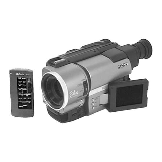
- Page 3 Supplied accessories 1 Wireless Remote Commander (1) 2 AC-L10A/L10B/L10C AC power adaptor 3 NP-F330 Battery pack (1) 4 CR2025 Lithium Battery (1) The lithium battery is already installed in your camcorder. 5 Size AA (R6) battery for Remote Commander (2) 6 A / V connecting cable (1) 7 Shoulder strap (1) 8 21 pin adaptor (1)
-
Page 4: To Take Out A Cassette When Not Eject (Force Eject)
SERVICE NOTE 1. POWER SUPPLY DURING REPAIRS In this unit, about 10 seconds after power is supplied (8.4V) to the battery terminal using the service power cord (J-6082-223-A), the power is shut off so that the unit cannot operate. Battery switch This following three methods are available to prevent this. -
Page 5: Self-Diagnosis Function
SELF-DIAGNOSIS FUNCTION 1. Self-diagnosis Function 2. Self-diagnosis display When problems occur while the unit is operating, the self-diagnosis When problems occur while the unit is operating, the counter of the function starts working, and displays on the viewfinder or Display viewfinder or Display window shows a 4-digit display consisting window what to do. -
Page 6: Self-Diagnosis Code Table
4. Self-diagnosis Code Table Self-diagnosis Code Symptom/State Correction Block Detailed Function Code Condensation. Remove the cassette, and insert it again after one hour. Clean with the optional cleaning cassette. Video head is dirty. Non-standard battery is used. Use the InfoLITHIUM battery. LOAD direction. -
Page 7: Table Of Contents
TABLE OF CONTENTS SERVICE NOTE 2. DISASSEMBLY Power Supply During Repairs ......... 4 2-1. Removal of Front Panel Block ......... 2-1 To Take out a Cassette when not Eject (Force Eject) ..4 2-2. Removal of Cabinet (R) Block ......... 2-2 2-3. - Page 8 4. PRINTED WIRING BOARDS AND SCHEMATIC 5. ADJUSTMENTS DIAGRAMS 5-1. CAMERA SECTION ADJUSTMENTS ......5-1 1-1. Preparations before Adjustment (Camera Section) ..5-1 4-1. Frame Schematic Diagram (1) ...........4-1 1-1-1. List of Service Tools ..........5-1 • Frame Schematic Diagram (2) ........4-4 1-1-2.
- Page 9 5-2. MECHANICAL SECTION ADJUSTMENT ....5-31 6. REPAIR PARTS LIST 2-1. Operating without a Cassette .......... 5-31 2-2. Tape path Adjustment .............5-31 6-1. Exploded Views ............6-1 Preparations for adjustments ........5-31 6-1-1. Cabinet (L) Block Assembly ........6-1 6-1-2. Front Panel Block Assembly ........6-2 5-3.
-
Page 40: Disassembly
CCD-TRV300E SECTION 2 DISASSEMBLY The equipment can be removed using the following procedure. VIDEO CAMERA RECORDER 2-8. CASSETTE LID ASSEMBLY 2-1. FRONT PANEL BLOCK 2-6. EVF BLOCK-2 2-2. CABINET (R) BLOCK 2-5. CF-54 BOARD AND CONTROL 2-3. EVF BLOCK-1 2-4. LCD BLOCK SWITCH BLOCK(PS-8990) 2-7. -
Page 41: Removal Of Cabinet (R) Block
2-2. REMOVAL OF CABINET (R) BLOCK 6 Connector CN933, 11P 5 Flat cable (FFC-236) CN911, 50P 1 Two screws (M2x4) 2 Three screws (M2x4) 3 Screw (M2x4) 4 Cabinet (R) assembly 2-3. REMOVAL OF EVF BLOCK-1 3 Tapping screw 2 CD shield sheet 5 VF base 4 Tapping screw 7 Three tapping screw... -
Page 42: Removal Of Lcd Block
2-4. REMOVAL OF LCD BLOCK 7 LCD block 6 Four tapping screws 4 Connector CN005,12P 2 Hinge cover assembly 3 Connector CN006,6P 1 Four tapping screws 5 Flexible board(control switch block PS-8990) CN002,14P 2-5. REMOVAL OF CF-54 BOARD AND CONTOROL SWITCH BLOCK (PS-8990) 8 Flat cable (FFC-236) CN001, 50P 7 Connector... -
Page 43: Removal Of Evf Block-2
2-6. REMOVAL OF EVF BLOCK-2 8 CRT holder assmebly 6 VF insulating sheet 9 CRT assembly 5 Remove the EVF rear cabinet assembly to the direction of arrow B . 2 Tapping screw 4 F lock screw (T) 3 Tapping screw 0 VF-104 board 7 Flexible flat cable(FCC-235) CN901,4P... -
Page 44: Removal Of Cassette Lid Assembly
2-8. REMOVAL OF CASSETTE LID ASSEMBLY 2-10. REMOVAL OF ZOOM LENS BLOCK 1 Two screws (M2x4) 4 FP-623 flexible board 2 Cassette lid assembly CN501, 16P 1 Two screws (M2x3) 6 Flexible connector CN551, 23P 5 FP-633 flexible board CN909, 10P 2 Screw (M2x3) 3 Zoom lens block 7 FP-635 flexible board... -
Page 45: Removal Of Vc-195 And Hp-104 Board
2-12. REMOVAL OF VC-195 AND HP-104 BOARDS 7 FP-631 flexible board 1 FP-220 flexible board CN903, 23P 2 Flexible board CN901, 8P from loading motor CN001, 16P !¡ Screw (M2x3) from video head 8 FP-621flexible board CN902, 12P 3 Flexible board CN905, 10P from drum motor 9 FP-635 flexible board... -
Page 46: Circuit Board Location
2-14. CIRCUIT BOARDS LOCATION CD-200 (CCD IMAGER) CF-54 (PANEL SWITCH) MA-332 (STEREO MIC) DD-105 (POWER) PJ-87 (AV OUT) VF-104 PD-92 (RGB DECODER, LCD, LCD DRIVE, BACK LIGHT) (B/W EVF) VP-48 (STEADY SHOT) VC-195 CAMERA, Y/C PROCESSOR, IN/OUT, HP-104 REC/PB HEAD AMP, SERVO/SYSTEM CONTROL, (HEADPHONE JACK) SERVO, AUDIO, MODE CONTROL... -
Page 47: Block Diagrams
CCD-TRV300E SECTION 3 BLOCK DIAGRAMS 3-1. OVERALL BLOCK DIAGRAM... -
Page 48: Camera/Video Block Diagram
CCD-TRV300E 3-2. CAMERA/VIDEO BLOCK DIAGRAM CAMERA REC 0.4Vp-p 0.3Vp-p CAMERA REC CAMERA REC IC001 TRIG : IC001 IC001 3Vp-p 0.4Vp-p CAMERA REC CAMERA REC IC001 0.3Vp-p IC202 CAMERA REC 0.5Vp-p 1.3Vp-p IC001 1.3Vp-p IC202 IC401 IC502 CAMERA REC 3.2Vp-p CAMERA REC 0.4Vp-p 2.9Vp-p 0.14usec... - Page 49 CCD-TRV300E 3-3. VTR/CAMEARA CONTROL BLOCK DIAGRAM 1.7Vp-p 20 MHz IC402 3Vp-p 13usec IC402 3Vp-p IC402 3Vp-p IC402 3Vp-p IC402 3-11 3-10...
-
Page 50: Servo Block Diagram
CCD-TRV300E 3-4. SERVO BLOCK DIAGRAM 3Vp-p 13usec 3Vp-p IC402 0.76Vp-p 2.8msec 506 kHz IC402 IC801 1.2Vp-p 5.6msec IC451 3Vp-p 3Vp-p 1.2msec 0.76Vp-p IC402 IC402 507 kHz IC801 3Vp-p 13usec IC402 3-12 3-13 3-14... -
Page 51: Mode Control Block Diagram
CCD-TRV300E CCD-TRV300E 3-5. MODE CONTROL BLOCK DIAGRAM 1.5Vp-p 20 MHz IC604 2.6Vp-p 32 kHz IC604 CAMERA REC 3Vp-p IC701 3-15 3-16 3-17 3-18... -
Page 52: Audio Block Diagram
CCD-TRV300E 3-6. AUDIO BLOCK DIAGRAM 0.4Vp-p IC301 CAMERA REC 0.36Vp-p IC301 CAMERA REC 0.26Vp-p 4.43 MHz IC301 CAMERA REC 2.9Vp-p IC301 3-19 3-20 3-21 3-22... -
Page 53: Lcd Block Diagram
CCD-TRV300E 3-7. LCD BLOCK DIAGRAM 4.7Vp-p IC5502 4.2Vp-p IC5502 0.7Vp-p IC5502 4.2Vp-p IC5502 4.2Vp-p IC5502 0.44Vp-p 0.2Vp-p IC5502 IC5502 0.2Vp-p IC5502 4.7Vp-p 4.1Vp-p IC5601 Approx.5.8MHz IC5601 4.7Vp-p Approx.2.9 MHz IC5601 4.7Vp-p IC5601 4.7Vp-p 20msec IC5601 3-25 3-23 3-24... -
Page 54: B/W Evf Block Diagram
CCD-TRV300E CCD-TRV300E 3-8. B/W EVF BLOCK DIAGRAM 2.2Vp-p IC901 1Vp-p IC901 3-26 3-27 3-28... -
Page 55: Power Block Diagram
CCD-TRV300E 3-9. POWER BLOCK DIAGRAM 3-29 3-30 3-31 3-32E... -
Page 56: Frame Schematic Diagram (1)
CCD-TRV300E SECTION 4 PRINTED WIRING BOARDS AND SCHEMATIC DIAGRAMS 4-1. FRAME SCHEMATIC DIAGRAM (1) FRAME (1) -
Page 57: Frame Schematic Diagram (2)
CCD-TRV300E FRAME SCHEMATIC DIAGRAM (2) FRAME (2) - Page 58 CCD-TRV300E 4-2. PRINTED WIRING BOARDS AND SCHEMATIC DIAGRAMS CD-200 (CCD IMAGER) PRINTED WIRING BOARD – Ref No. CD-200 BOARD: 8,000 series – THIS NOTE IS COMMON FOR PRINTED WIRING BOARDS AND SCHEMATIC DIAGRAMS. (In addition to this, the necessary note is printed in each block.) CD-200 BOARD (SIDE B) CD-200 BOARD (SIDE A) •...
- Page 59 CCD-TRV300E CCD-TRV300E VC-195 (CAMERA, Y/C PROCESSOR, IN/OUT, REC/PB HEAD AMP, SERVO/SYSTEM CONTROL, SERVO, AUDIO, MODE CONTROL) PRINTED WIRING BOARD VC-195 BOARD – Ref No. VC-195 BOARD: 1,000 series – (SIDE B) VC-195 BOARD (SIDE B) C002 C213 C481 C774 L156 Q454 R112 R428...
- Page 60 CCD-TRV300E CCD-TRV300E VC-195 BOARD (SIDE A) VC-195 BOARD (SIDE A) C328 C-11 CN908 A-17 R074 C-12 R527 B-17 C001 A-13 C004 A-14 C330 C-11 CN909 G-11 R075 C-13 R529 E-12 CN911 D-17 R081 D-13 R551 G-11 C004 B-13 C331 C-11 C005 B-14 C332...
- Page 61 CCD-TRV300E CCD-TRV300E VC-195 BOARD (1/9) CAMERA REC 2.3Vp-p 28.375 MHz IC501 CAMERA REC 2.3Vp-p 14.18 MHz IC501 11 12 CAMERA REC 7Vp-p IC501 CAMERA REC 7Vp-p IC501 CAMERA REC 3Vp-p IC501 CAMERA REC 3Vp-p IC501 CAMERA REC 3.2Vp-p 0.14usec IC502 —...
- Page 62 CCD-TRV300E CCD-TRV300E • For schematic diagrams. • Refer to page 4–11 for Printed Wiring Board. 4-19 4-20 4-21 4-22 CAMERA (2) VC-195 (2/9)
- Page 63 CCD-TRV300E • For schematic diagrams. • Refer to page 4–11 for Printed Wiring Board. VC-195 BOARD (3/9) CAMERA REC CAMERA REC 0.34Vp-p 3.1Vp-p 4.43 MHz IC202 IC202 CAMERA REC CAMERA REC 0.84Vp-p 3Vp-p IC202 IC202 CAMERA REC CAMERA REC 0.5Vp-p 3Vp-p IC202 IC202...
- Page 64 CCD-TRV300E CCD-TRV300E • For schematic diagrams. • Refer to page 4–11 for Printed Wiring Board. VC-195 BOARD (4/9) CAMERA REC 0.46Vp-p IC151 0.32Vp-p IC151 1.4Vp-p IC151 17 64 1.8Vp-p IC151 25 60 IC151 (2.1Vp-p) IC151 (1.6Vp-p) 4-29 4-30 4-27 4-28 IN/OUT VC-195 (4/9)
- Page 65 CCD-TRV300E • For schematic diagrams. • Refer to page 4–11 for Printed Wiring Board. VC-195 BOARD (5/9) CAMERA REC CAMERA REC 0.3Vp-p 7Vp-p 4.12 MHz IC001 Q001 CAMERA REC 0.3Vp-p IC001 TRIG : IC001 0.4Vp-p IC001 0.4Vp-p IC001 0.4Vp-p IC001 CAMERA REC 2.9Vp-p IC001...
- Page 66 CCD-TRV300E • For schematic diagrams. VC-195 BOARD (6/9) • Refer to page 4–11 for Printed Wiring Board. CAMERA REC 1.7Vp-p 20 MHz IC402 3Vp-p IC402 3Vp-p IC402 3Vp-p IC402 3Vp-p 13usec IC402 3Vp-p 13usec IC402 3Vp-p 13usec IC402 3Vp-p 1.2msec IC402 3Vp-p 2.8msec...
- Page 67 CCD-TRV300E • For schematic diagrams. • Refer to page 4–11 for Printed Wiring Board. 4-38 4-39 4-40 SERVO VC-195 (7/9)
- Page 68 CCD-TRV300E CCD-TRV300E • For schematic diagrams. VC-195 BOARD (7/9) • Refer to page 4–11 for Printed Wiring Board. CAMERA REC VC-195 BOARD (8/9) CAMERA REC 2.9Vp-p 1.2Vp-p 5.6msec IC451 IC301 3Vp-p 0.4Vp-p IC451 IC301 CAMERA REC 0.36Vp-p 3Vp-p 2.8msec IC301 IC451 CAMERA REC 0.26Vp-p...
- Page 69 CCD-TRV300E CCD-TRV300E • For schematic diagrams. • Refer to page 4–11 for Printed Wiring Board. VC-195 BOARD (9/9) 1.5Vp-p 20 MHz IC604 2.6Vp-p 32 kHz IC604 4-45 4-46 4-47 4-48 MODE CONTROL VC-195 (9/9)
- Page 70 CCD-TRV300E VP-48 (STEADY SHOT) PRINTED WIRING BOARDS – Ref No. VP-48 BOARD: 8,000 series – VP-48 BOARD VP-48 BOARD (SIDE B) VP-48 BOARD (SIDE A) C601 Q601 C602 Q602 C603 Q603 C604 Q604 C605 C606 R601 C607 R602 C608 R603 C609 R604 C610...
- Page 71 CCD-TRV300E HP-104 (HEADPHONE JACK) MA-332 (STEREO MIC) PRINTED WIRING BOARD PRINTED WIRING BOARD – Ref No. HP-104 BOARD: 8,000 series – – Ref No. MA-332 BOARD: 8,000 series – MA-332 BOARD (SIDE B) MA-332 BOARD (SIDE A) HP-104 BOARD (SIDE B) HP-104 BOARD (SIDE A) 1-669-004- HP-104 BOARD...
- Page 72 CCD-TRV300E 4-57 4-59 4-58 STEREO MIC MA-332...
-
Page 73: Control Switch Block (Fk-8500/Ss-8500)
CCD-TRV300E 4-60 4-61 4-62 CONTROL SWITCH BLOCK, PANEL SWITCH PS-8990 CF-54... - Page 74 CCD-TRV300E CF-54 (PANEL SWITCH) PRINTED WIRING BOARD – Ref No. CF-54 BOARD: 8,000 series – CF-54 BOARD (SIDE B) CF-54 BOARD (SIDE A) CF-54 BOARD BZ001 B-16 R020 BZ002 B-16 R022 R023 C001 A-14 R024 C002 A-14 R025 B-14 C003 C-12 R026 R029...
- Page 75 CCD-TRV300E PD-92 (RGB DECODER, LCD DRIVE, BACK LIGHT, LCD) PRINTED WIRING BOARD – Ref No. PD-92 BOARD: 10,000 series – PD-92 BOARD (SIDE B) PD-92 BOARD (SIDE A) PD-92 BOARD C5501 B-10 D5604 C-10 R5542 R5673 C5502 B-10 D5701 R5544 R5674 C5503 D5702...
- Page 76 CCD-TRV300E CCD-TRV300E PD-92 BOARD (1/4) CAMERA REC 0.44Vp-p IC5502 0.2Vp-p IC5502 0.2Vp-p IC5502 0.7Vp-p IC5502 4.7Vp-p IC5502 4.2Vp-p IC5502 4.2Vp-p IC5502 4.2Vp-p IC5502 4-69 4-70 4-71 RGB DECODER PD-92 (1/4)
- Page 77 CCD-TRV300E • For schematic diagrams. • Refer to page 4–67 for Printed Wiring Board. PD-92 BOARD (2/4) CAMERA REC 4.7Vp-p IC5601 4.7Vp-p 20msec IC5601 4.7Vp-p Approx. 2.9MHz IC5601 4.1Vp-p Approx. 5.8MHz IC5601 4.7Vp-p 20msec IC5601 4.7Vp-p IC5601 4-72 4-73 4-74 LCD DRIVE PD-92 (2/4)
- Page 78 CCD-TRV300E • For schematic diagrams. • For schematic diagrams. • Refer to page 4–67 for Printed Wiring Board. • Refer to page 4–67 for Printed Wiring Board. PD-92 BOARD (4/4) CAMERA REC 2.9Vp-p 24.17 kHz IC5801 4-75 4-76 4-77 BACK LIGHT, LCD PD-92 (3/4, 4/4)
-
Page 79: Board
CCD-TRV300E PJ-87 (AV OUT) PRINTED WIRING BOARD – Ref No. PJ-87 BOARD: 8,000 series – PJ-87 BOARD (SIDE B) PJ-87 BOARD C101 C102 C103 C104 C105 C106 C107 C108 C109 C110 C111 CN101 D101 D102 D103 D105 D106 D107 J101 L101 L102 L103... - Page 80 CCD-TRV300E VF-104 (B/W EVF) PRINTED WIRING BOARD – Ref No. VF-104 BOARD: 4,000 series – VF-104 BOARD VF-104 BOARD (SIDE B) VF-104 BOARD (SIDE A) C901 C902 C903 C904 C905 C906 C907 C908 C909 C910 C911 C912 C913 C914 C915 C916 CN901 CN902...
- Page 81 CCD-TRV300E CCD-TRV300E DD-105 (POWER) PRINTED WIRING BOARD – Ref No. DD-105 BOARD: 2,000 series – DD-105 BOARD (SIDE B) DD-105 BOARD (SIDE A) DD-105 BOARD C801 L801 R823 C802 L802 R824 C803 L803 R825 C804 L804 R826 C805 L805 R827 C806 L806 R828...
- Page 82 CCD-TRV300E DD-105 BOARD CAMERA REC 0.76Vp-p 507 kHz IC801 0.76Vp-p 506 kHz IC801 4-87 4-88 4-89 4-90E POWER DD-105...
-
Page 83: Adjustments
CCD-TRV300E SECTION 5 ADJUSTMENTS 5-1. CAMERA SECTION ADJUSTMENTS 1-1. PREPARATIONS BEFORE ADJUSTMENT (CAMERA SECTION) 1-1-1. List of Service Tools • Oscilloscope • Color monitor • Vectorscope • Adjusting driver • Regulated power supply • Digital voltmeter Ref. No. Usage Name Parts Code Filter for color temperature correction J-6080-058-A... -
Page 84: Preparations
1-1-2. Preparations Note 1: For details of how remove the cabinet and boards, refer to “2. DISASSEMBLY”. Note 2: When performing only the adjustments, the lens block and boards need not be disassembled. 1) Connect the equipment for adjustments according to Fig. 5-1-3. 2) The flont panel block (MA-332 board, focus ring, microphone Pattern box unit) need not be assembled. - Page 85 Color monitor Vector scope Terminated at 75 Ω Lens block CD-200 board CN401 Regulaterd power supply (8.4 ± 0.1 Vdc) Battery terminal (Note 1) Extension cable(16P) (J-6082-357-A) VP-48 board CN602 Adjusting Need not connected remote VIDEO terminal commander Battery switch LANC CN935 jack...
-
Page 86: Setting The Switch
1-1-3.Precaution 1. Setting the Switch Unless otherwise specified, set the switches as follows and perform adjustments without loading cassette. 1. POWER switch ............CAMERA 9. SHUTTER SPEED (CF-54 board) ........Auto 2. DEMO MODE (Menu display) ........OFF 10. IRIS (CF-54 board) ............Auto 3. -
Page 87: Adjusting Remote Commander
1-1-4. Adjusting Remote Commander • Changing the address The adjusting remote commander is used for changing the The address increases when the FF ()) button is pressed, calculation coefficient in signal processing, EVR data, etc. The and decreases when the REW (0) button is pressed. There adjusting remote commander performs bi-directional are altogether 256 addresses, from 00 to FF. -
Page 88: Data Processing
1-1-5. Data Processing The calculation of the DDS display and the adjusting remote calculate and convert the result to hexadecimal notation, and use it commander display data (hexadecimal notation) are required for as the adjustment data. Table 5-1-2. indicates the hexadecimal obtaining the adjustment data of some adjustment items. -
Page 89: Initialization Of D, E, F
2. Modification of D, E, F Page Data 1-2. INITIALIZATION OF D, E, F PAGE DATA If the D, E, F page data has been initialized, change the data of the 1. Initializing the D,E,F Page Data “Fixed data-2” address shown in the following tables by manual Note 1: If “Initializing the D, E, F Page Data”... -
Page 90: D Page Table
3. D Page Table Note1 : Fixed data-1 : Initialized data. (Refer to “1. Initializing the D,E,F Page Data”.) Fixed data-2 : Modified data. (Refer to “2. Modification of D, E, F Page Data”). Address Initial Value Remark Address Initial Value Remark Fixed data-1 00 to 0F Fixed data-1... -
Page 91: F Page Table
4. F Page table Address Initial Value Remark Note 1: Flange back adj. Fixed data-1 : Initialized data. ( Refer to “1. Initializing the D,E,F Page Data”.) Fixed data-2 : Modified data. (Refer to “2. Modification of D, E, F Page Data”). Steady shot adj. - Page 92 Address Initial Value Remark Address Initial Value Remark Fixed data-1 Switching position adj. Fixed data-1 Fixed data-2 Fixed data-1 Fixed data-2 Fixed data-2 Fixed data-1 Fixed data-1 Fixed data-2 Fixed data-1 Fixed data-2 Fixed data-1 Fixed data-2 Fixed data-1 Fixed data-2 Fixed data-1 Fixed data-2 Fixed data-1...
-
Page 93: E Page Table
5. E Page Table Address Initial Value Remark Note 1: Fixed data-2 Fixed data-1 : Initialized data. ( Refer to “1. Initializing the D,E,F Page Data”.) Fixed data-2 : Modified data. Fixed data-1 (Refer to “2. Modification of D, E, F Page Data”). Note 2: See “1-5. - Page 94 Address Initial Value Remark Address Initial Value Remark Note 2 Color adj. (LCD) Fixed data-2 Fixed data-1 Fixed data-1 Fixed data-2 Fixed data-2 Fixed data-1 Fixed data-1 Fixed data-2 Fixed data-1 Fixed data-2 Fixed data-1 Fixed data-2 Fixed data-1 Fixed data-2 Fixed data-1 Fixed data-2 FC to FF...
-
Page 95: Camera System Adjustments
1-3. CAMERA SYSTEM ADJUSTMENTS Before perform the camera system adjustments, Check that the specified value of “28MHz Origin Oscillation Adjustment”, “Y OUT level Adjustment” and “C OUT level Adjustment” of “VIDEO SYSTEM ADJUSTMENT” are satisfied. 1. G-CAM flip Adjustment Set the color reproduction conditions to optimum. Subject Color bar chart standard picture frame Measurement Point... -
Page 96: Hall Adjustment
2. HALL Adjustment For detecting the position of the lens iris, adjust the hall AMP gain and offset. Subject Not required Measurement Point DDS display data of LCD or TV monitor (Note 3) Measuring Instrument Adjustment Page Adjustment Address 2F, 30 Specified Value 96 to 9A during IRIS OPEN (Note 1) 1C to 20 during IRIS CLOSE (Note 2) -
Page 97: Flange Back Adjustment
3. Flange Back Adjustment 3-2. Flange Back Adjustment (2) The inner focus lens flange back adjustment is carried out Perform this adjustment after performing “Flange Back Adjustment automatically. In whichever case, the focus will be deviated during (1)”. auto focusing/manual focusing. Subject Subject more than 500m away 3-1. -
Page 98: Flange Back Check
4. Flange Back Check 5. Picture Frame Setting Subject Siemens star Subject Color bar chart standard picture frame (2.0 m from the front of the protection (1.5m from the front of the protection glass) glass) (Luminance: approx. 200 lux) Measurement Point Video output terminal Measurement Point Check operation on TV monitor... -
Page 99: Color Reproduction Adjustment
6. Color Reproduction Adjustment Adjust the color Separation matrix coefficient so that proper color reproduction is produced. Burst position Subject Color bar chart standard picture frame Measurement Point Video output terminal Measuring Instrument Vectorscope Adjustment Page Adjustment Address 34, 36, F5, F6 Specified Value All color luminance points should settle within each color reproduction frame. -
Page 100: Iris In/Out Adjustment
7. IRIS IN/OUT Adjustment 8. MAX GAIN Adjustment For the unit to judge if the white balance is indoors or outdoors in Setting the minimum illumination. auto white balance operations, measure the light level and write it If it is not consistent, the image level required for taking subjects in in the EEPROM. -
Page 101: Auto White Balance Standard Data Input
9. Auto White Balance Standard Data Input 10. Auto White Balance Adjustment Adjust to the proper auto white balance output data. Subject Clear chart If it is not correct, auto white balance and color reproducibility will (Color bar standard picture frame) be poor. -
Page 102: White Balance Check
11. White Balance Check Subject Clear chart (Color bar standard picture frame) Filter Filter C14 for color temperature correction ND filter 1.0 and 0.3 2 mm Measurement Point video output terminal Measuring Instrument Vectorscope Specified Value Fig. 5-1-10. A to C Checking method: 1) Check that the lens is not covered with either filter. -
Page 103: Steady Shot Adjustment
12. Steady Shot Adjustment Adjusting method: • Perform the steady shot adjustment only when replacing the 1) Expose pattern A with the zoom TELE end. angular velocity sensor. When the microprocessor, circuit, etc. Note: Digital zoom (Menu display) ....... OFF malfunctions, do not perform this adjustment but check operations only. -
Page 104: Steady Shot Adjustment (2)
12-2. Steady Shot Adjustment (2) Adjusting method: 1) Expose pattern B with the zoom TELE end. Subject Pattern B Note: Digital zoom (Menu display) ....... OFF Measurement Point Video output terminal 2) Adjust the inclination of the camera so that the horizontal black Measuring Instrument Oscilloscope line comes to the center of the screen. -
Page 105: Monochrome Electronic Viewfinder System Adjustments
1-4. MONOCHROME ELECTRONIC VIEWFINDER SYSTEM ADJUSTMENTS 1-4-2. Centering Adjustment 1-4-1. Horizontal Slant Check Mode Playback Mode Playback Signal Alighment tape : Signal Alighment tape : For checking operations For checking operations (WR5-8CSE) (WR5-8CSE) Monoscope section Monoscope section ± 4% ± 1.5 ° Specified Value Specified Value Adjusting method:... -
Page 106: Aberration Adjustment
1-4-4. Aberration Adjustment 1-4-5. Horizontal Amplitude Adjustment (VF-104 board) Mode VTR stop Signal Dot pattern Mode Playback Specified Value b1 2 • a1 Signal Alighment tape : b2 0.8 • a2 For checking operations (WR5-8CSE) Adjusting method: Monoscope section 1) Adjust the aberration adjustment ring so that the tracing of the Adjusting Element C909 (SOL901) dot satisfies the specified value. -
Page 107: Vertical Amplitude Adjustment (Vf-104 Board)
1-4-6. Vertical Amplitude Adjustment (VF-104 board) 1-4-7. Brightness Adjustments (VF-104 board) Mode Playback Mode Playback Signal Alighment tape : Signal Alighment tape : For checking operations For checking operations (WR5-8CSE) (WR5-8CSE) Monoscope section Monoscope section Adjusting Element RV903 Specified Value RV904 10 ±... -
Page 108: Lcd System Adjustment
1-5. LCD SYSTEM ADJUSTMENT 1. LCD Initial Data Input Note1: The back light (fluorescent tube) is driven by a high voltage Mode VTR stop AC power supply. Therefore, do not touch the back light Signal Arbitrary holder to avoid electrical shock. Adjustment Page Note2: When replacing the LCD unit, be careful to prevent Adjustment Address... -
Page 109: Vco Adjustment (Pd-92 Board)
2. VCO Adjustment (PD-92 board) 3. D range Adjustment (PD-92 board) Set the VCO freerun frequency. If deviated, the LCD screen will be Set the D range of the RGB decoder used to drive the LCD to the blurred. specified value. If deviated, the LCD screen will become blackish or saturated (whitish). -
Page 110: Bright Adjustment (Pd-92 Board)
4. Bright Adjustment (PD-92 board) 5. Contrast Adjustment (PD-92 board) Set the level of the VIDEO signal for driving the LCD to the specified Set the level of the VIDEO signal for driving the LCD to the specified value. If deviated, the screen image will be blackish or saturated value. -
Page 111: V-Com Level Adjustment (Pd-92 Board)
6. V-COM Level Adjustment (PD-92 board) 7. Color Adjustment (PD-92 board) Set the common electrode drive signal level of LCD to the specified Set the color saturation to the standard value. If deviated, the color value. will be to dark or light. Mode VTR stop Mode... -
Page 112: V-Com Adjustment (Pd-92 Board)
8. V-COM Adjustment (PD-92 board) 9. White Balance Adjustment (PD-92 board) Set the DC bias of the common electrode drive signal of LCD to the Correct the white balance. specified value. If deviated, the LCD screen color cannot be reproduced. If deviated, the LCD display will move, producing flicker and Mode VTR stop... -
Page 113: Mechanical Section Adjustment
5-2. MECHANICAL SECTION ADJUSTMENT 6) Connect the oscilloscope. Channel 1: Pin 6 of CN910 of VC-195 board External trigger: Pin !¡ of CN910 of VC-195 board Mechanism Parts Adjustments Connect the oscilloscope via the CPC-7 jig For details on the adjustments and checks of mechanical section (J-6082-382-A). -
Page 114: Video Section Adjustments
5-3. VIDEO SECTION ADJUSTMENTS When performing adjustments, refer to the layout diagrams for adjustment related parts beginning from page 5-54. 3-1. PREPARATIONS BEFORE ADJUSTMENT The following adjusting instruments are used for adjusting the video section. 3-1-1. Equipments to be Used 1) TV monitor 2) Oscilloscope: 2 phenomena, band 30 MHz or wider, with delay mode. -
Page 115: Precautions On Adjusting
3-1-2. Precautions on Adjusting 3-1-3. Adjusting Connectors 1) The adjustments of this unit are performed in the VTR mode or Some of the adjusting points of the video section are concentrated camera mode. at VC-195 board CN910. Connect the measuring instruments via To set to the VTR mode, set the power switch to “PLAYER”... -
Page 116: Connecting The Equipments
3-1-4. Connecting the Equipments Connect the measuring instruments as shown in Fig. 5-3-2 and perform the adjustments. Connecting the TV Monitor and Regulated Power Supply Battery terminal Main Unit TV monitor Regulated power supply 8.4 ± 0.1Vdc VIDEO Connect when using the camera mode or playing back. -
Page 117: Input/Output Level And Impedance
Note: Measure using the VIDEO terminal (Terminated at 75 Ω). Fig. 5-3-3. shows the 75% color bar signals recorded on the alignment tape. Fig. 5-3-3. Color Bar Signals of the Alignment Tape 3-1-6. Input/Output Level and Impedance Video input/output Phono jack, 1 Vp-p, 75Ω, unbalanced, sync negative S video input/output 4-pin mini DIN... -
Page 118: Service Mode
3-1-8. Service Mode 2. Emergency Memory Address Additional note on adjustment Page F Address 10 to 1B Note: After the completion of the all adjustments, cancell the service mode by either of the following ways. Address Contents 1st EMG code 1) Unplug the main power supply and remove the lithium battery. -
Page 119: Msw Codes
2-2. MSW Codes • The lower parts of the data of addresses 12, 16 and 1A represent the MSW codes (mode switch, mechanism position) when errors occurs. • The upper parts of the data of addresses 12, 16 and 1A represent, when the mechanism position is to be moved, the MSW codes at the start of movement (when moving the loading motor). -
Page 120: Bit Value Discrimination
3. Bit value discrimination 4. Switch check (1) Bit values must be discriminated using the display data of the Page 3 Address 43 adjusting remote commander for the following items. Use the table below to discriminate if the bit value is “1” or “0”. Function When bit value=1 When bit value=0 0 VTR MODE SW... -
Page 121: Switch Check (2)
5. Switch check (2) Page 3 Address 60 to 66 Using method: 1) Select page: 3, address: 60 to66. 2) By discriminating the display data, the pressed key can be discriminated. Data Address 00 to 0D 0E to 29 2A to 46 47 to 68 69 to 90 91 to BE... -
Page 122: Led, Lcd (Display Window) Check
8. LED, LCD (display window) check 9. Record of Use Check Page 3 Address 05 Bit5 Page 3 Address A2 to AA Address Using method: Function Remarks 1) Select page: 3, address: 05, and set the bit value of Bit5 to “1”. 1000th place digit and 2) Check that all LED are lit and all segments of LCD (display 100th place digit of... -
Page 123: System Control System Adjustment
3-2. SYSTEM CONTROL SYSTEM ADJUSTMENT 1. Initialization of D, E, F Page Data If the D, E, F page data is erased due to some reason, perform “1-2. INITIALIZATION OF D, E, F PAGE DATA”, of “5-1. CAMERA SECTION ADJUSTMENT”. 2. -
Page 124: Servo System Adjustments
3-3. SERVO SYSTEM ADJUSTMENTS 2. Switching Position Adjustment (VC-195 Board) If deviated in this case causes switching noise or jitter on the played 1. CAP FG Offset Adjustment (VC-195 board) back screen. Improve the capstan servo characteristic. If it is not correct. jitters Mode Playback will increase. -
Page 125: Video System Adjustments
3-4. VIDEO SYSTEM ADJUSTMENTS 2. AFC f0 Adjustment (VC-195 board) Adjust the pull-in range of the A/D converted clock generator during Video system adjustments must be performed in the following order. playback. Mode VTR stop [Adjusting Order] Signal No signal 1. -
Page 126: Filter F0 Adjustment (Vc-195 Board)
3. Filter f0 Adjustment (VC-195 board) 4. Y OUT Level Adjustment (VC-195 board) Minimize the chroma signal residual components during composite Set the Y signal output level. video signal input. Mode VTR stop Mode VTR stop Signal No signal Signal No signal Measurement Point Y signal terminal of S VIDEO... -
Page 127: C Out Level Adjustment (Vc-195 Board)
5. C OUT Level Adjustment (VC-195 board) 6. RP Filter f0 Adjustment (VC-195 board) Set the chroma signal output level. Adjust the LPF of the playback RF amplifier. Mode VTR stop Mode VTR stop Signal No signal Signal No signal Pin 9 of CN910 (RF AGC OUT) Measurement Point Chroma signal terminal of S VIDEO... -
Page 128: Rec Y Current Adjustment (Vc-195 Board)
7. REC Y Current Adjustment (VC-195 board) 10) Write the following data in page: F, address: 57 to 5A. Adjust the Y FM signal recording current. Address Data Mode VTR recording (SP mode) Signal No signal Pin !º of CN910 (REC RF) Measurement Point Measuring Instrument Oscilloscope (20 MHz BW LIMIT: OFF) - Page 129 8. REC L Level Adjustment (VC-195 board) 9) Write the following data in page: F, address: 63 to 64. Set the recording levels of the REC AFM signal and REC ATF signal. Address Data If the level is too low, the audio S/N will deteriorated, tracking will not be stable, or SP/LP will not be discriminated properly.
-
Page 130: Rec C Current Adjustment (Vc-195 Board)
9. REC C Current Adjustment (VC-195 board) Processing after completed adjustment: Set the recording current levels of the REC Chroma signal. If it is 1) Select page: 0, address: 01, and set data: 01. too low, chroma signal noise in played back picture will increased. 2) Select page: D, address: 14, and set the data memorized at step If too high, Y signal noises will increase and white modulation noises 2) of “Preparations”. -
Page 131: Stereo Audio System Adjustment
3-5. STEREO AUDIO SYSTEM ADJUSTMENT [Connecting the measuring instruments for the audio] Connect the audio system measuring instruments in addition to the • The items to be adjusted for the R channel will be indicated video system measuring instruments as shown in Fig. 5-3-15, and within the [ ], in regard to the adjusting items to be adjusted for perform adjustments at the power switch [PLAYER] position. -
Page 132: Mhz Deviation Adjustment (Vc-195 Board)
1. 1.5 MHz Deviation Adjustment (VC-195 board) Processing after completed adjustment: Sets the spectrum of the L-ch ((L+R)/2 signal) level modulated 1) Select page: 0, address: 01, and set data: 01. during recording. If deviated, the crosstalk signal of the audio signal 2) Select page: D, address: 14, and set the data memorized at step will occur and the audio level will drop during both playback and 2) of “Preparations”. -
Page 133: Mhz Deviation Adjustment (Vc-195 Board)
2. 1.7 MHz Deviation Adjustment (VC-195 board) Processing after completed adjustment: Sets the spectrum of the R-ch ((L-R)/2 signal) level modulated during 1) Select page: 0, address: 01, and set data: 01. recording. If deviated, the crosstalk signal of the audio signal will 2) Select page: D, address: 14, and set the data memorized at step occur and the audio level will drop during both playback and 2) of “Preparations”. -
Page 134: Bpf F0 Adjustment (Vc-195 Board)
3. BPF f0 Adjustment (VC-195 board) Sets the BPF passing frequency so that the AFM signal can separate from the playback RF signal properly. If deviated. the mono/stereo mode will be differentiated incorrectly, and noises and distortions will increase during high volume playback. Mode Playback Signal... -
Page 135: Arrangement Diagram For Adjustment Parts
3-6. ARRANGEMENT DIAGRAM FOR ADJUSTMENT PARTS VC-195 BOARD (SIDE A) CN909 CN551 CN501 IC604 IC202 CN911 C085 IC001 IC301 VC-195 BOARD (SIDE B) IC501 CN910 IC751 5-54E... -
Page 136: Repair Parts List
CCD-TRV300E SECTION 6 REPAIR PARTS LIST 6-1. EXPLODED VIEWS The components identified by NOTE: mark ! or dotted line with mark • Items marked “*” are not stocked since they are ! are critical for safety. seldom required for routine service. Some delay Replace only with part number should be anticipated when ordering these items. -
Page 137: Front Panel Block Assembly
6-1-2. FRONT PANEL BLOCK ASSEMBLY MIC901 MIC902 not supplied Ref. No. Part No. Description Remark Ref. No. Part No. Description Remark X-3948-528-1 PANEL (899) ASSY, FRONT 3-988-943-01 GEAR, MF A-7073-531-A MA-332 BOARD, COMPLETE 3-988-944-01 BRACKET, MF X-3948-527-1 GRILLE (899) ASSY, MICROPHONE MIC901 1-542-312-11 MICROPHONE (L-CH) 1-475-626-11 SWITCH BLOCK, CONTROL (MF-8990) MIC902 1-542-312-11 MICROPHONE (R-CH) -
Page 138: Cabinet (R) Block Assembly
6-1-3. CABINET (R) BLOCK ASSEMBLY supplied supplied SP901 not supplied Ref. No. Part No. Description Remark Ref. No. Part No. Description Remark 3-965-367-01 SPACER, SP 3-948-339-61 TAPPING 1-783-240-11 CABLE, FLEXIBLE FLAT (FFC-236) 1-475-627-11 SWITCH BLOCK, CONTROL (PS-8990) 3-988-870-11 LID (899), LITHIMU BATTERY A-7073-532-A CF-54 BOARD, COMPLETE 3-948-339-01 SCREW,TAPPING X-3948-519-1 CABINET (R) (899) ASSY... -
Page 139: Lcd Block Assembly
6-1-4. LCD BLOCK ASSEMBLY ND801 LCD901 ND802 not supplied The components identified by mark ! or dotted line with mark ! are critical for safety. Replace only with part number specified. Ref. No. Part No. Description Remark Ref. No. Part No. Description Remark 3-987-625-01 COVER (M), HINGE... - Page 140 6-1-5. EVF BLOCK ASSEMBLY (B/W EVF) V901 The components identified by mark ! or dotted line with mark ! are critical for safety. Replace only with part number specified. Ref. No. Part No. Description Remark Ref. No. Part No. Description Remark X-3944-966-1 FINDER ASSY 1-783-241-11 CABLE, FLEXIBLE FLAT (FFC-235)
-
Page 141: Main Boards Assembly
6-1-6. MAIN BOARDS BLOCK ASSEMBLY Ref. No. Part No. Description Remark Ref. No. Part No. Description Remark * 258 3-987-716-01 PROTECTOR, LS FLEXIBLE A-7073-481-A DD-105(VH1) BOARD, COM PLETE 3-713-786-21 SCREW (M2X3) 3-987-711-01 FRAME (A), MD A-7093-468-A VC-195(XVRE) BOARD, COMPLETE 1-668-957-11 FP-621 FLEXIBLE BOARD 3-987-675-01 FRAME (B), MD 3-962-826-01 SCREW (2X4) A-7073-530-A PJ-87(H) BOARD, COMPLETE... -
Page 142: Battery Panel And Lens Block Assembly
6-1-7. BATTERY PANEL AND LENS BLOCK ASSEMBLY IC401 SE602 not supplied SE601 not supplied not supplied J901 Be sure to read “Note on the CCD Imager replacement” on page 4–9 when changing the CCD imager. Ref. No. Part No. Description Remark Ref. -
Page 143: Zoom Lens (Vcl-4020Vb)
6-1-8. ZOOM LENS (VCL-4020VB) M905 Ref. No. Part No. Description Remark Ref. No. Part No. Description Remark 3-709-275-01 SCREW 3-709-276-01 TUBE, MIRROR UNIT, MAIN 3-707-946-01 SCREW (BT(3)P1.7X4.5) A-7030-815-A VAP UNIT ASSY M905 3-709-277-01 MOTOR, FOCUS... -
Page 144: Cassette Compartment Assembly
6-1-9. CASSETTE COMPARTMENT ASSEMBLY LS CHASSIS BLOCK SECTION (See page 6-10) MECHANISM CHASSIS BLOCK SECTION (See page 6-11) Ref. No. Part No. Description Remark Ref. No. Part No. Description Remark A-7040-421-A DAMPER ASSY X-3945-399-1 GEAR ASSY, GOOSENECK 7-624-102-04 STOP RING 1.5, TYPE -E 3-947-503-01 SCREW (M1.4X2.5) X-3945-400-X CASSETTE COMPARTMENT ASSY 3-331-007-21 WASHER... -
Page 145: Ls Chassis Assembly
6-1-10. LS CHASSIS ASSEMBLY S002 S001 D001 FP-249 (not supplied) Ref. No. Part No. Description Remark Ref. No. Part No. Description Remark A-7040-419-A BASE (S) BLOCK ASSY, GUIDE 3-965-563-01 GEAR, T SOFT A-7040-418-B BASE (T) BLOCK ASSY, GUIDE 3-965-559-01 STOPPER (T) 3-965-565-01 CLAW, T SOFT 3-965-557-01 STOPPER (T), GB X-3945-397-1 DECK ASSY, REEL, S... -
Page 146: Mechanism Chassis Assembly
6-1-11. MECHANISM CHASSIS ASSEMBLY M901 81 1 M903 M902 S901 not supplied not supplied Ref. No. Part No. Description Remark Ref. No. Part No. Description Remark X-3947-343-1 GROUND (IM) ASSY, SHAFT 3-965-535-01 SPRING (LIMITTER ARM S), COIL 3-965-550-02 SCREW (M1.7X1.6) 3-965-542-01 SHIELD, MOTOR 1-657-785-11 FP-248 FLEXIBLE BOARD (DEW SENSOR) 3-965-539-01 GEAR (A) -
Page 147: Electrical Parts List
CD-200 CF-54 6-2. ELECTRICAL PARTS LIST Note: • Due to standardization, replacements in the parts list • SEMICONDUCTORS The components identified by mark ! In each case, u: µ , for example: may be different from the parts specified in the or dotted line with mark ! are critical uA...: µ... - Page 148 CF-54 DD-105 Ref. No. Part No. Description Remark Ref. No. Part No. Description Remark S006 1-771-029-31 SWITCH, TACTILE (PICTURE EFFECT) C844 1-135-157-21 TANTALUM CHIP 10uF 6.3V S007 1-762-851-21 SWITCH, KEY BOARD (IRIS) C846 1-135-157-21 TANTALUM CHIP 10uF 6.3V S010 1-771-029-31 SWITCH, TACTILE (MENU) C847 1-164-506-11 CERAMIC CHIP 4.7uF...
- Page 149 DD-105 Ref. No. Part No. Description Remark Ref. No. Part No. Description Remark D935 8-719-045-87 DIODE MA4Z082WA-(TX). Q817 8-729-041-24 TRANSISTOR NDS355AN D936 8-719-045-87 DIODE MA4Z082WA-(TX). D938 8-719-420-14 DIODE MA8082-M Q819 8-729-043-94 TRANSISTOR CPH3106-PM-TL Q820 8-729-037-74 TRANSISTOR UN9213J-(TX).SO < FERRITE BEAD > Q823 8-729-037-74 TRANSISTOR UN9213J-(TX).SO Q824...
- Page 150 DD-105 FP-249 Ref. No. Part No. Description Remark Ref. No. Part No. Description Remark R821 1-218-879-11 RES,CHIP 0.50% 1/16W R902 1-216-864-11 METAL CHIP 1/16W R822 1-216-150-91 RES,CHIP 1/8W R903 1-216-845-11 METAL CHIP 100K 1/16W R824 1-216-837-11 METAL CHIP 1/16W R825 1-218-879-11 RES,CHIP 0.50% 1/16W R904...
- Page 151 1-779-334-11 CONNECTOR, FFC/FPC 20P L454 1-216-295-91 SHORT 0 CN305 1-691-483-21 CONNECTOR, FFC/FPC 4P < DIODE > A-7073-531-A MA-332 BOARD, COMPLETE D303 8-719-061-82 DIODE TLSU1002(TPX1,SONY) D305 8-719-404-49 DIODE MA111 ********************** (Ref. No. 8,000 Series) D321 8-719-420-14 DIODE MA8082-M D322 8-719-420-14 DIODE MA8082-M <...
- Page 152 MA-332 PD-92 Ref. No. Part No. Description Remark Ref. No. Part No. Description Remark R341 1-216-821-11 METAL CHIP 1/16W C5607 1-164-004-11 CERAMIC CHIP 0.1uF R342 1-216-832-11 METAL CHIP 8.2K 1/16W C5608 1-164-357-11 CERAMIC CHIP 1000PF R343 1-216-829-11 METAL CHIP 4.7K 1/16W C5610 1-162-926-11 CERAMIC CHIP...
- Page 153 PD-92 PJ-87 Ref. No. Part No. Description Remark Ref. No. Part No. Description Remark Q5601 8-729-402-42 TRANSISTOR UN5213 R5660 1-216-864-11 METAL CHIP 1/16W Q5602 8-729-402-42 TRANSISTOR UN5213 R5661 1-216-864-11 METAL CHIP 1/16W Q5605 8-729-230-63 TRANSISTOR 2SC4116-YG R5669 1-216-864-11 METAL CHIP 1/16W Q5606 8-729-420-24 TRANSISTOR 2SB1218A-QRS...
- Page 154 PJ-87 VC-195 Ref. No. Part No. Description Remark Ref. No. Part No. Description Remark < DIODE > C028 1-135-259-11 TANTAL. CHIP 10uF 6.3V C029 1-162-970-11 CERAMIC CHIP 0.01uF D101 8-719-059-57 DIODE MAZJ082DFLSO D102 8-719-059-57 DIODE MAZJ082DFLSO C030 1-162-970-11 CERAMIC CHIP 0.01uF D103 8-719-059-57 DIODE MAZJ082DFLSO...
- Page 155 VC-195 Ref. No. Part No. Description Remark Ref. No. Part No. Description Remark C166 1-162-970-11 CERAMIC CHIP 0.01uF C309 1-135-318-11 TANTAL. CHIP 33uF C168 1-109-982-11 CERAMIC CHIP C310 1-104-847-11 TANTAL. CHIP 22uF C169 1-109-982-11 CERAMIC CHIP C170 1-162-970-11 CERAMIC CHIP 0.01uF C312 1-107-823-11 CERAMIC CHIP...
- Page 156 VC-195 Ref. No. Part No. Description Remark Ref. No. Part No. Description Remark C418 1-164-156-11 CERAMIC CHIP 0.1uF C523 1-115-467-11 CERAMIC CHIP 0.22uF C419 1-164-156-11 CERAMIC CHIP 0.1uF C524 1-162-962-11 CERAMIC CHIP 470PF C420 1-162-970-11 CERAMIC CHIP 0.01uF C451 1-107-826-11 CERAMIC CHIP 0.1uF C525 1-162-970-11 CERAMIC CHIP...
- Page 157 VC-195 Ref. No. Part No. Description Remark Ref. No. Part No. Description Remark C703 1-162-970-11 CERAMIC CHIP 0.01uF FB203 1-414-228-11 INDUCTOR CHIP 0UH C704 1-162-924-11 CERAMIC CHIP 56PF FB204 1-414-228-11 INDUCTOR CHIP 0UH C705 1-162-970-11 CERAMIC CHIP 0.01uF C706 1-162-923-11 CERAMIC CHIP 47PF FB205 1-414-228-11 INDUCTOR CHIP 0UH...
- Page 158 VC-195 Ref. No. Part No. Description Remark Ref. No. Part No. Description Remark L203 1-414-754-11 INDUCTOR 10uH Q217 8-729-037-53 TRANSISTOR 2SB1462J-QR(TX).SO Q301 8-729-042-74 TRANSISTOR UN9216J-(K8).SO L204 1-410-658-31 INDUCTOR CHIP 220uH Q302 8-729-042-74 TRANSISTOR UN9216J-(K8).SO L205 1-412-955-11 INDUCTOR 22uH Q305 8-729-037-63 TRANSISTOR UN9115J-(K8).SO L206 1-412-945-11 INDUCTOR 3.3uH...
- Page 159 VC-195 Ref. No. Part No. Description Remark Ref. No. Part No. Description Remark R045 1-216-845-11 METAL CHIP 100K 1/16W R165 1-216-803-11 METAL CHIP 1/16W R046 1-216-821-11 METAL CHIP 1/16W R166 1-216-804-11 METAL CHIP 1/16W R049 1-216-833-11 METAL CHIP 1/16W R167 1-216-803-11 METAL CHIP 1/16W R170...
- Page 160 VC-195 Ref. No. Part No. Description Remark Ref. No. Part No. Description Remark R257 1-216-295-91 SHORT R430 1-216-813-11 METAL CHIP 1/16W R302 1-216-817-11 METAL CHIP 1/16W R431 1-216-825-11 METAL CHIP 2.2K 1/16W R432 1-216-845-11 METAL CHIP 100K 1/16W R303 1-216-817-11 METAL CHIP 1/16W R433 1-216-845-11 METAL CHIP...
- Page 161 VC-195 Ref. No. Part No. Description Remark Ref. No. Part No. Description Remark R525 1-216-864-11 METAL CHIP 1/16W R641 1-216-845-11 METAL CHIP 100K 1/16W R526 1-216-864-11 METAL CHIP 1/16W R642 1-216-821-11 METAL CHIP 1/16W R643 1-216-857-11 METAL CHIP 1/16W R527 1-216-864-11 METAL CHIP 1/16W R644...
- Page 162 VC-195 VF-104 Ref. No. Part No. Description Remark Ref. No. Part No. Description Remark < CONNECTOR > R715 1-216-829-11 METAL CHIP 4.7K 1/16W R716 1-216-819-11 METAL CHIP 1/16W CN901 1-573-506-41 CONNECTOR, FPC (NON ZIF) 4P CN902 1-573-290-21 PIN, CONNECTOR (1.5MM) (SMD)4P R717 1-216-821-11 METAL CHIP 1/16W...
- Page 163 VF-104 VP-48 Ref. No. Part No. Description Remark Ref. No. Part No. Description Remark < TRANSFORMER > < IC > ! T901 1-453-124-11 TRANSFORMER ASSY, FLYBACK IC601 8-759-359-49 IC NJM3414AV(TE2) IC602 8-759-359-49 IC NJM3414AV(TE2) < THERMISTOR > IC603 8-759-058-43 IC NJM3404AV(TE2) IC604 8-759-489-19 IC uPC6756GR-8JG-E2 TH901...
-
Page 164: A / V Connecting
VP-48 Ref. No. Part No. Description Remark Ref. No. Part No. Description Remark R639 1-216-839-11 METAL CHIP 1/16W S002 1-572-688-11 SWITCH, PUSH (1 KEY) (C.C. LOCK) R640 1-216-839-11 METAL CHIP 1/16W S003 1-572-688-11 SWITCH, PUSH (1 KEY) (EJECT) R641 1-216-839-11 METAL CHIP 1/16W S901 1-762-436-15 SWITCH, ROTARY (ENCODER) - Page 165 < PARTS REFERENCE SHEET > Take a copy CAMERA COLOR REPRODUCTION FRAME and Parts reference sheets with a clear sheet for use. You can find the parts position of mount locations applying to boards of a set. S I D E B CN909 CN551 I C 2 0 4...
- Page 166 FOR CAMERA COLOR REPRODUCTION ADJUSTMENT Take a copy CAMERA COLOR REPRODUCTION FRAME and Parts reference sheets with a clear sheet for use. CCD-TRV300E...
- Page 167 CCD-TRV300E Sony Corporation 98C0941-1 Printed in Japan © 1998. 3 9-974-057-11 Personal A&V Products Company Published by Quality Engineering Dept. – 266 – (Osaki East)
Need help?
Do you have a question about the Handycam Vision CCD-TRV300E and is the answer not in the manual?
Questions and answers