Sony DSR-250 Service Manual
Hide thumbs
Also See for DSR-250:
- Operating instructions manual (192 pages) ,
- Service manual (130 pages) ,
- Brochure & specs (6 pages)
Table of Contents
Advertisement
Quick Links
SERVICE MANUAL
SERVICE MANUAL
NTSC model : DSR-250
PAL model
: DSR-250P
Video camera
recorder
System
Video recording system
2 rotary heads
Helical scanning system
Audio recording system
Rotary heads, PCM system
Quantization: Fs32 kHz (12 bits,
channels 1/2, channels 3/4),
Fs48 kHz (16 bits, channels 1/2)
Video signal
NTSC color, EIA standards (DSR-250),
PAL colour, CCIR standards
(DSR-250P)
Usable cassette
DVCAM cassette with the
mark printed
Mini DVCAM cassette with the
mark printed
DV cassette with the
mark
printed
Mini DV cassette with the
mark printed
Tape speed
DVCAM format:
Approx. 28.218 mm/s
DV format SP mode: Approx.
18.812 mm/s
Recording/playback time
DVCAM format: 184 min (using
cassette PDV-184ME)
DV format SP mode: 270 min
(using cassette PDV-184ME)
Fast-forward/rewind time
Approx. 45 s (using cassette
DVM60/PDVM-40ME)
Approx. 2 min 30 s (using cassette
PDV-184ME)
DSR-250/250P
Ver 1.3 2003. 01
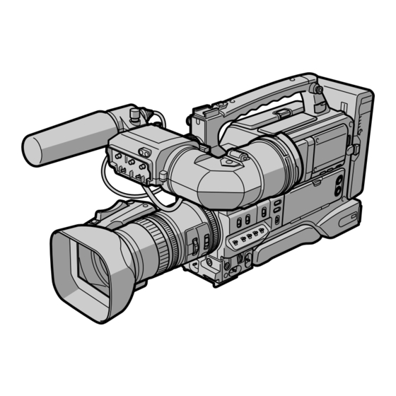
Photo : DSR-250
SPECIFICATIONS
Viewfinder
Electric viewfinder (B&W)
Image device
1/3 type CCD (3 Charge Coupled
Device) Approx. 380 000 pixels
(Effective: Approx. 340 000 pixels)
(DSR-250), Approx. 450 000 pixels
(Ef
fective: Approx. 400 000 pixels)
(DSR-250P)
Lens
Combined power zoom lens
Filter diameter 58 mm (2 3/8 in)
12× (Optical), 48× (Digital)
F1.6 - 2.4
Focal length
6 - 72 mm (1/4 - 2 7/8 in)
When converted to a 35 mm still
camera
43.2 - 518.4 mm (1 3/4 - 20 1/2 in)
Colour temperature
Auto, nIndoor (3 200 K),
Outdoor (5 800 K),
(A, B)
Minimum illumination
2 lux (F1.6)
Input/Output connectors
VIDEO IN/OUT
Input/output auto switch
RCA pin-jack, 1 Vp-p, 75 ohms,
unbalanced, sync negative
S VIDEO
Input/output auto switch
4-pin mini DIN
Luminance signal: 1 Vp-p,
75 ohms, unbalanced
Chrominance signal: 0.286 Vp-p
(DSR-250), 0.3 Vp-p (DSR-250P),
75 ohms, unbalanced
RMT-811
AUDIO IN/OUT CH-1/CH-2
Input/output auto switch
RCA pin-jack, 245 mV, (at output
impedance more than 47 kilohms)
Output impedance with less than
2.2 kilohms
Input impedance more than
47 kilohms
AUDIO IN CH1/CH2
XLR 3-pin, female
–60 dBu: 6.8 kilohms,
+4 dBu: 6.8 kilohms
(0 dBu = 0.775 Vrms)
PHONES
Stereo minijack (ø 3.5 mm)
LANC control jack
Stereo mini-minijack (ø 2.5 mm)
MIC IN +48V
XLR 3-pin, female
VF
20-pin
LIGHT
2-pin
DV IN/OUT
6-pin connector
Speaker
Dynamic speaker (ø 20 mm)
DC IN 12V
XLR 4-pin, female
DC OUT 12V
4-pin, male
LCD screen
Picture
2.5 type measured diagonally
49.9 × 37.3 mm (2 × 1 1/2 in)
Total dot number
200 640 (880 × 228)
DIGITAL CAMCORDER
RMT-811
US Model
Canadian Model
DSR-250
AEP Model
Chinese Model
DSR-250P
R MECHANISM
General
Peak inrush current (DSR-250P)
(1) Hot switching inrush current,
measured in accordance with
European standard EN55103-1:
6.3 A (230 V)
Power requirements
14.4 V (Lithium-ion battery pack)
12 to 17 V (AC power adaptor)
Average power consumption
(when using the battery pack)
During camera recording using
LCD
12.1 W
Viewfinder
10.5 W
Operating temperature
0 °C to 40 °C (32 °F to 104 °F)
Storage temperature
–20 °C to +60 °C (–4 °F to +140 °F)
Dimensions (approx.)
242 × 251 × 509 mm (9 5/8 × 10 ×
20 1/8 in) (w/h/d)
Mass (approx.)
3.5 kg (7 lb 11 oz)
main unit only
4.9 kg (10 lb 13 oz)
including the BP-L40 (A) battery
pack, cassette PDV-184ME,
microphone, viewfinder, and
hood cap
Supplied accessories
See page 2.
— Continued on next page —
Advertisement
Table of Contents

Subscribe to Our Youtube Channel
Related Manuals for Sony DSR-250


Summary of Contents for Sony DSR-250
- Page 1 System European standard EN55103-1: (Effective: Approx. 340 000 pixels) 2.2 kilohms Video recording system 6.3 A (230 V) (DSR-250), Approx. 450 000 pixels Input impedance more than 2 rotary heads Power requirements fective: Approx. 400 000 pixels) 47 kilohms Helical scanning system 14.4 V (Lithium-ion battery pack)
-
Page 2: Supplied Accessories
CRITIQUES POUR LA SÉCURITÉ DE FONCTIONNEMENT. NE COMPONENTS WITH SONY PARTS WHOSE PART NUMBERS REMPLACER CES COMPOSANTS QUE PAR DES PIÈSES SONY APPEAR AS SHOWN IN THIS MANUAL OR IN SUPPLEMENTS DONT LES NUMÉROS SONT DONNÉS DANS CE MANUEL OU PUBLISHED BY SONY. -
Page 3: Table Of Contents
TABLE OF CONTENTS SERVICE NOTE Superimposing a title ··························································· 1-27 Making your own titles ························································ 1-28 TO TAKE OUT A CASSETTE WHEN NOT EJECT Labelling a cassette ······························································ 1-29 (FORCE EJECT) ································································ 8 Erasing the cassette memory data ········································ 1-29 Customizing Your Camcorder SELF-DIAGNOSIS FUNCTION Changing the menu settings ·················································... -
Page 4: Schematic Diagrams
3-7. POWER BLOCK DIAGRAM (2/4) ······························ 3-13 • VI-156 (CAMERA, DV/MS INTERFACE, SERVO, 3-8. POWER BLOCK DIAGRAM (3/4) ······························ 3-15 REC/PB HEAD AMP, AUDIO, DD CONV.) 3-9. POWER BLOCK DIAGRAM (4/4) ······························ 3-17 PRINTED WIRING BOARD ······················· 4-63 • MS-058 (MS CONNECTOR) PRINTED WIRING BOARDS AND PRINTED WIRING BOARD ·······················... - Page 5 • XL-003 (CH1/CH2 MIC AMP) Color Reproduction Adjustment (ND Filter 2) ·············· 5-25 SCHEMATIC DIAGRAM ·························· 4-113 White Balance Check ···················································· 5-26 • DD-146 (DC-DC CONVERTER), Steady Shot Adjustment ················································ 5-27 DC-095 (DC OUT) 20-1. Steady Shot Adjustment (1) ··········································· 5-28 PRINTED WIRING BOARDS ···················...
- Page 6 2-3-19. MD-76 BOARD AND ENCODER RETAINER ········ 5-49 4-4. Processing after Completing Adjustments ···················· 5-69 2-3-20. COMPONENTS OF GL ARM S/T ASSEMBLY PLL f & LPF f Final Adjustment (VI-156 board) ······· 5-69 (GL ARM ASSEMBLY, GL HELICAL TORSION 3-4. VIDEO SYSTEM ADJUSTMENTS ····························· 5-70 SPRING, GL GEAR) ····················································...
- Page 7 1-3. Replacement of VF Loupe ········································ 1-3 (E) 1-4. Replacement of Outside Holder T and Eyepiece Outer Ring ································································ 1-4 (E) 1-5. Changing the Viewfinder Correspond to Left Eye ·· 1-5 (E) 1-6. Recommended Replacement Parts ··························· 1-5 (E) Alignment 2-1.
-
Page 8: Service Note
SERVICE NOTE TO TAKE OUT A CASSETTE WHEN NOT EJECT (FORCE EJECT) 1 Refer to 2-6. to remove the cabinet (L) assembly. 2 Remove the shoulder pad. 3 Remove the CN4300 (2P) of VI-156 board. 4 Remove the CN501 (2P) of VI-156 board. 5 Supply +4.5V from the DC power supply to the cam motor and unload the tape guide. -
Page 9: Self-Diagnosis Function
SELF-DIAGNOSIS FUNCTION SELF-DIAGNOSIS FUNCTION SELF-DIAGNOSIS DISPLAY When problems occur while the unit is operating, the counter of the When problems occur while the unit is operating, the self-diagnosis function starts working, and displays on the viewfinder or LCD viewfinder or LCD screen consists of an alphabet and 4-digit screen what to do. -
Page 10: Self-Diagnosis Code Table
SELF-DIAGNOSIS CODE TABLE Self-diagnosis Code Block Detailed Symptom/State Correction Function Code Condensation. Remove the cassette, and insert it again after one hour. Video head is dirty. Clean with the optional cleaning cassette. LOAD direction. Loading does not Load the tape again, and perform operations from the beginning. complete within specified time UNLOAD direction. -
Page 11: General
DSR-250/250P SECTION 1 This section is extracted from GENERAL instruction manual. (DSR-250P) - Page 20 1-10...
- Page 21 1-11...
- Page 22 1-12...
- Page 23 1-13...
- Page 24 1-14...
- Page 25 1-15...
- Page 26 1-16...
- Page 27 1-17...
- Page 28 1-18...
- Page 29 1-19...
- Page 30 1-20...
- Page 31 1-21...
- Page 32 1-22...
- Page 33 1-23...
- Page 34 1-24...
- Page 35 1-25...
- Page 36 1-26...
- Page 37 1-27...
- Page 38 1-28...
- Page 39 1-29...
- Page 40 1-30...
- Page 41 1-31...
- Page 42 1-32...
- Page 43 1-33...
- Page 44 1-34...
- Page 45 1-35...
- Page 46 1-36...
- Page 47 1-37...
- Page 48 1-38...
- Page 49 1-39...
- Page 50 1-40...
- Page 51 1-41...
- Page 52 1-42...
- Page 53 1-43...
- Page 54 1-44...
- Page 55 1-45...
- Page 56 1-46...
- Page 57 1-47...
-
Page 58: Auto Logo Insert For Copyright Protection
This section is extracted from instruction manual. (Auto Logo Insert for Copyright Protection) 1-48... - Page 59 1-49...
- Page 60 1-50...
- Page 61 1-51E...
-
Page 62: Disassembly
DSR-250/250P SECTION 2 DISASSEMBLY The following flow chart shows the disassembly procedure. 2-1. LCD section PD-126 board service position (PD-126 board, Inverter transformer unit) 2-2. Carrying handle section (TH-010, ME-019 boards, VF shoe base) 2-3. VF section (MAIN, SUB boards) -
Page 63: Lcd Section
NOTE: Follow the disassembly procedure in the numerical order given. 2-1. LCD SECTION (PD-126 BOARD, INVERTER TRANSFORMER UNIT) Two screws (M2 × 4), lock ace, p2 Two screws (M2 × 4), cabinet (C) lock ace, p2 REMOVING THE PD-126 BOARD, Two screws (M2 ×... -
Page 64: Carrying Handle Section (Th-010, Me-019 Boards, Vf Shoe Base)
2-2. CARRYING HANDLE SECTION (TH-010, ME-019 BOARDS, VF SHOE BASE) REMOVING VF SHOE BASE Rear handle Carrying handle cover assembly block assembly Two screws (M2 × 4), lock ace, p2 Two screws (M3 × 8) Lock ring (D), Screw Two screws (M2 ×... -
Page 65: Vf Section (Main, Sub Boards)
2-3. VF SECTION (MAIN, SUB BOARDS) Refer to the separate DXF-801/810CE Service Manual (attach to the end of this manual) [ Section 1. Service Information ]. VF assembly DXF-801 (DSR-250), Two screws (M3 × 6) DXF-801CE (DSR-250P) Two screws (M3 × 8) -
Page 66: Cabinet (R) Block Assembly (Sw-343 Board)
2-4. CABINET (R) BLOCK ASSEMBLY (SW-343 BOARD) FP-245 flexible board (10P) Cabinet (R) block assembly Two screws (M3 × 8) Two screws (M3 × 8) REMOVING THE SW-343 BOARD VR knob Screw (M2 × 3), lock ace, p2 SW protection sheet Seven screws (M2 ×... -
Page 67: Hinge Section (Hinge Assembly, Fp-241 Flexible Board)
2-5. HINGE SECTION (HINGE ASSEMBLY, FP-241 FLEXIBLE BOARD) REMOVING HARNESS (PS-111) (14P), HARNESS (PS-110) (8P) Remove the harness Harness (PS-111) (14P),harness (PS-110) (8P) (PS-110) (8P) in the Harness direction of the arrow. (PS-111) (14P) When removing it, be careful not Three screws (M2 ×... -
Page 68: Cabinet (L) Assembly, Mechanism Deck
2-6. CABINET (L) ASSEMBLY, MECHANISM DECK 6 Flexible board (from capstan motor) (18P) 7 Flexible board (from drum motor) (11P) Four screws Five screws (M3 × 8) (M3) step Harness (from loading motor) (2P) Mechanism 9 Flexible board (from drum motor) (10P) deck Harness (from cam motor) (2P) -
Page 69: Boards
2-7. DD-146, IN-057 BOARDS DD-146 board Two screws (M2 × 3), lock ace, p2 Two screws (M2 × 3), lock ace, p2 IN-057 board [DD-146, IN-057 BOARDS SERVICE POSITION] How to make the DC cable (See page 2-1) AC IN Regulated power supply DD-146 board IN-057 board... -
Page 70: Board
2-8. VI-156 BOARD 4 FVK-001 flexible flat cable (8P) 5 Harness (VL-054) (6P) Harness (VH-050) (12P) 6 Harness (MV-124) (7P) 7 Harness (VM-068) (12P) 8 Harness (VG-052) (12P) VI-156 board 9 Harness (VF-071) (3P) 2 Two screws (M2 × 3), lock ace, p2 qd FP-243 flexible board (27P) -
Page 71: Lens Block Assembly
2-9. LENS BLOCK ASSEMBLY (ON-001, NO-001 BOARDS, CONTROL SWITCH BLOCK (CF-1044)) Mi ring assembly, Control switch block (EG-1044) (6P) Three screws (M2 × 6) lock ace, p2 Screw (M3 × 8) Screw (M3 × 8) Lens block assembly Two screws (M3 ×... -
Page 72: Lens Block Assembly (Lens Cabinet (R))
2-10.LENS BLOCK ASSEMBLY (LENS CABINET (R)) CAUTION WHEN INSTALLING AND REMOVING SCREWS When you want to remove screws, remove this screw first. Also remove this screw last when re-installing the parts. Two screws (M2 × 4), Two screws (M2 × 4), lock ace, p2 Screw (M2 ×... - Page 73 [SERVICE POSITION TO CHECK THE CAMERA SECTION] Connection to Check the CAMERA Section To check the CAMERA Section, set the CAMERA to the "forced CAMERA power ON" mode. Setting the “Forced CAMERA Power ON” mode Exiting the “Forced CAMERA Power ON” mode 1) Select page: 0, address: 01, and set data: 01.
- Page 74 2-11.XL-003, VO-012, DV-031, RL-057 BOARDS VO-012 board, DV-031 board Two screws (M2 × 3) lock ace, p2 Screw (M2 × 3) lock ace, p2 XL-003 board, XLR bracket, AU slide knob Two screws (M3 × 8) RL-057 board, LANC bracket REMOVING XL-003 BOARD 2-12.FS-082 BOARD, 4P CONNECTOR (WITH DC SW) Two screws (M2.6 ×...
- Page 75 (from loading motor) (2P) Harness D Flexible board (from drum motor) (10P) (MV-124) (7P) VF assembly Harness (from cam motor) (2P) DXF-801 (DSR-250), F FRV-008 flexible flat cable DXF-801CE (DSR-250P) ME-019 board (from MD-76 board) (21P) G FRV-008 flexible flat cable...
- Page 76 2-13.CIRCUIT BOARDS LOCATION The circuit boards contained in the mechanism deck and that in the zoom lens are not shown. KY-049 (VCR FUNCTION) TH-010 EJ-034 (SIRCS (REAR)) (EJECT) HP-129 LL-010 (HEADPHONE OUT) (USER FUNCTION) PD-126 VL-034 (RGB DRIVE, TIMING GEN) (LIGHT) INVERTER TRANSFORMER UNIT...
-
Page 77: Flexible Boards Location
2-14.FLEXIBLE BOARDS LOCATION The flexible boards contained in the mechanism deck and that in the zoom lens are not shown. CONTROL SWITCH BLOCK (EG-1044) FKE-001 FVK-001 FVS-001 CONTROL SWITCH BLOCK (CF-1044) FP-241 FP-245 FSS-004 FRV-008 FP-243 FP-242 2-16E... -
Page 78: Block Diagrams
DSR-250/250P SECTION 3 BLOCK DIAGRAMS 3-1. OVERALL BLOCK DIAGRAM (1/5) ( ) : Page No. shown in ( ) indicates the page to refer on the schematic diagram. CD-274 BOARD VI-156 BOARD(1/5) (4-9) (4-9) IC103 AGC CONT 1,2 R,B GAIN... -
Page 79: Overall Block Diagram (2/5)
DSR-250/250P 3-2. OVERALL BLOCK DIAGRAM (2/5) ( ) : Page No. shown in ( ) indicates the page to refer on the schematic diagram. CN162 VI-156 BOARD(2/5) DV IN/OUT (4-21) (4-17) X301 24.576MHz SPCK IC301 IC1407 CN010 CN161 (4-23) SPCK... -
Page 80: Overall Block Diagram (3/5)
DSR-250/250P 3-3. OVERALL BLOCK DIAGRAM (3/5) ( ) : Page No. shown in ( ) indicates the page to refer on the schematic diagram. R MECHA DECK (SEE PAGE 4-39) (4-32) (4-36) (4-33) VI-156 BOARD(3/5) IC4501 IC102 IC4500 (1/2) REC CK... -
Page 81: Overall Block Diagram (4/5)
DSR-250/250P 3-4. OVERALL BLOCK DIAGRAM (4/5) ( ) : Page No. shown in ( ) indicates the page to refer on the schematic diagram. SW-343 KY-049 BOARD VI-156 BOARD(4/5) EJ-034 (SEE PAGE 4-85) IC1104 (4-45) (4-46) BOARD(1/2) BOARD S271 S270... -
Page 82: Overall Block Diagram (5/5)
DSR-250/250P 3-5. OVERALL BLOCK DIAGRAM (5/5) ( ) : Page No. shown in ( ) indicates the page to refer on the schematic diagram. IN-057 BOARD SW-343 BOARD(2/2) VI-156 BOARD(5/5) DD-146 BOARD (SEE PAGE 4-93,94) (SEE PAGE 4-119) CN303 IC501... - Page 83 DSR-250/250P 3-6. POWER BLOCK DIAGRAM (1/4) ( ) : Page No. shown in ( ) indicates the page to refer on the schematic diagram. IN-057 CN243 CN303 POWER CONT BOARD LIGHT CONT (SEE PAGE 4-119) PS304 HI UNREG J9001 PS302...
- Page 84 DSR-250/250P 3-7. POWER BLOCK DIAGRAM (2/4) ( ) : Page No. shown in ( ) indicates the page to refer on the schematic diagram. VI-156 BOARD(1/3) SHOE ON AU VCC POWER BLOCK(4/4) 8.4V (SEE PAGE 3-17) UNREG 12V VTR DD ON...
- Page 85 DSR-250/250P 3-8. POWER BLOCK DIAGRAM (3/4) ( ) : Page No. shown in ( ) indicates the page to refer on the schematic diagram. RL-157 BOARD VI-156 BOARD(2/3) (SEE PAGE 4-78) J141 LANC DC LANC DC LANC CN009 CN141 UNREG 12V...
- Page 86 DSR-250/250P 3-9. POWER BLOCK DIAGRAM (4/4) ( ) : Page No. shown in ( ) indicates the page to refer on the schematic diagram. PD-126 BOARD MD-76 BOARD (4-58) PANEL 4.6V LCD901 (SEE PAGE 4-71) PANEL 2.8V Q2102,2104 ME-019 BOARD IC2501 PANEL 13.5V...
- Page 87 DSR-250/250P SECTION 4 PRINTED WIRING BOARDS AND SCHEMATIC DIAGRAMS 4-1. FRAME SCHEMATIC DIAGRAM (1/3) CN500 50P CN025 50P VDDB SUBB IMAGER SE-116 SE601 SE600 PITCH BOARD LENS B_CCD_OUT CD-274 BOARD UNIT IMAGER PS_REF V2AB V2BB PSD_OUT VDD2B SE_VCC IMAGER V2AR...
- Page 88 DSR-250/250P FRAME SCHEMATIC DIAGRAM (2/3) SB-036 BOARD S066 S061 DISPLAY ZEBRA S067 SPOT LIGHT S068 BACK LIGHT FP-241 FLEXIBLE S065 MODE AUDIO LEVEL DISPLAY S521 (RVS) S522 ND901 BACK-LIGHT (OPEN/CLOSE) 2.5INCH COLOR LCD901 PM-040 BOARD UNIT S081 MODE CAMERA CN503...
- Page 89 DSR-250/250P FRAME SCHEMATIC DIAGRAM (3/3) VIEWFINDER ME-019 BOARD CN703 DM-141 MIC_GND MIC_GND DD-146 BOARD HARNESS MIC_+48V MIC_+48V EVF_GND VL-034 BOARD EVF_GND EVF_+12V CN701 EVF_+12V FRONT MIC CN302 DD-063 CN301 CN481 HARNESS LIGHT_OUT LIGHT_OUT CN482 LIGHT_GND LIGHT_GND LIGHT_OUT CN483 LIGHT LIGHT_GND...
- Page 90 DSR-250/250P DSR-250/250P 4-2. PRINTED WIRING BOARDS AND SCHEMATIC DIAGRAMS THIS NOTE IS COMMON FOR WIRING BOARDS AND SCHEMATIC DIAGRAMS (In addition to this, the necessary note is printed in each block) (For printed wiring boards) (Measuring conditions voltage and waveform) •...
- Page 91 DSR-250/250P For Schematic Diagram • Refer to page 4-11 for printed wiring board. • Refer to page 4-121 for waveforms. CD-274 BOARD C130 L100 CCD IMAGER 0.1u 100uH SIGNAL PATH -REF.NO.:1000 SERIES- C102 XX MARK:NO MOUNT VIDEO SIGNAL NO MARK:REC/PB MODE...
- Page 92 DSR-250/250P CD-274 (CCD IMAGER) PRINTED WIRING BOARD — Ref. No. CD-274 Board; 1,000 Series — For printed wiring board • Refer to page 4-125 for parts location. • CD-274 board consists of multiple layers. However, only the sides (layers) A and B are shown.
- Page 93 DSR-250/250P For Schematic Diagram • Refer to page 4-63 for printed wiring board. • Refer to page 4-121 for waveforms. VI-156 BOARD(1/25) CAMERA-1(CH BLOCK) C759 C721 0.1u -REF.NO.:10000 SERIES- XX MARK:NO MOUNT C724 C726 R710 0.1u 0.1u NO MARK:REC/PB MODE...
- Page 94 DSR-250/250P For Schematic Diagram • Refer to page 4-63 for printed wiring board. • Refer to page 4-122 for waveforms. VI-156 BOARD(2/25) CAMERA (U-CORE BLOCK) -REF.NO.:10000 SERIES- XX MARK:NO MOUNT IRIS_COM IRIS_COM NO MARK:REC/PB MODE R :REC MODE DIR_0A P :PB MODE...
- Page 95 DSR-250/250P For Schematic Diagram • Refer to page 4-63 for printed wiring board. • Refer to page 4-122 for waveforms. VI-156 BOARD(3/25) MS INTERFACE(MS BLOCK) -REF.NO.: 10000 SERIES- IC1405_VCC TO(4/25) XX MARK:NO MOUNT NO MARK:REC/PB MODE R :REC MODE P :PB MODE...
- Page 96 DSR-250/250P For Schematic Diagram • Refer to page 4-63 for printed wiring board. • Refer to page 4-122 for waveform. VI-156 BOARD(4/25) NO MARK:REC/PB MODE R :REC MODE RS232C I/F,STILL CONTROL(MS BLOCK) P :PB MODE -REF.NO.:10000 SERIES- XX MARK:NO MOUNT...
- Page 97 DSR-250/250P For Schematic Diagram • Refer to page 4-63 for printed wiring board. • Refer to page 4-122 for waveforms. VI-156 BOARD(5/25) NO MARK:REC/PB MODE R :REC MODE TO(22/25) DV SIGNAL PROCESSOR P :PB MODE TD_3-4 -REF.NO.: 10000 SERIES- TD_3-4...
- Page 98 DSR-250/250P For Schematic Diagram • Refer to page 4-63 for printed wiring board. • Refer to page 4-122 for waveforms. VI-156 BOARD(6/25) DV INTERFACE(JC-2 BLOCK) NO MARK:REC/PB MODE R :REC MODE -REF.NO.: 10000 SERIES- P :PB MODE XX MARK:NO MOUNT...
- Page 99 DSR-250/250P For Schematic Diagram • Refer to page 4-63 for printed wiring board. • Refer to page 4-123 for waveforms. VI-156 BOARD(7/25) NO MARK:REC/PB MODE LINE IN/OUT(IO BLOCK) R :REC MODE P :PB MODE -REF.NO.: 10000 SERIES- XX MARK:NO MOUNT A_4.6V...
- Page 100 DSR-250/250P For Schematic Diagram • Refer to page 4-63 for printed wiring board. • Refer to page 4-123 for waveforms. VI-156 BOARD(8/25) NO MARK:REC/PB MODE R :REC MODE LINE A/D CONV(IN BLOCK) P :PB MODE -REF.NO.:10000 SERIES- XX MARK:NO MOUNT...
- Page 101 DSR-250/250P For Schematic Diagram • Refer to page 4-63 for printed wiring board. • Refer to page 4-123 for waveform. VI-156 BOARD(9/25) MECHA CONTROL(MC BLOCK) -REF.NO.: 10000 SERIES- C508 XX MARK:NO MOUNT 6.3V REG_GND NO MARK:REC/PB MODE TO(25/25) R517 R :REC MODE ±...
- Page 102 DSR-250/250P For Schematic Diagram • Refer to page 4-63 for printed wiring board. • Refer to page 4-123 for waveforms. VI-156 BOARD(10/25) NO MARK:REC/PB MODE R :REC MODE SIGNAL PATH SERVO(CM BLOCK) P :PB MODE -REF.NO.: 10000 SERIES- REC/PB XX MARK:NO MOUNT...
- Page 103 DSR-250/250P For Schematic Diagram • Refer to page 4-63 for printed wiring board. • Refer to page 4-123 for waveforms. VI-156 BOARD(11/25) NO MARK:REC/PB MODE R :REC MODE SERVO-2(CM BLOCK) P :PB MODE -REF.NO.: 10000 SERIES- XX MARK:NO MOUNT CAP_VS...
- Page 104 DSR-250/250P For Schematic Diagram • Refer to page 4-63 for printed wiring board. • Refer to page 4-123 for waveforms. VI-156 BOARD(12/25) REC/PB HEAD AMP SIGNAL PATH -REF.NO.: 10000 SERIES- VIDEO SIGNAL XX MARK:NO MOUNT AUDIO CHROMA Y/CHROMA SIGNAL NO MARK:REC/PB MODE...
- Page 105 DSR-250/250P For Schematic Diagram • Refer to page 4-63 for printed wiring board. • Refer to page 4-123 for waveforms. VI-156 BOARD(13/25) CAMERA (MC-3 BLOCK) NO MARK:REC/PB MODE R :REC MODE -REF.NO.: 10000 SERIES- P :PB MODE XX MARK:NO MOUNT...
- Page 106 DSR-250/250P For Schematic Diagram • Refer to page 4-63 for printed wiring board. HALL_AD TO(13/25) VI-156 BOARD(14/25) IRIS_PWM ZOOM/FOCUS DRIVE(LA BLOCK) R162 R157 2200 -REF.NO.:10000 SERIES- XX MARK:NO MOUNT C148 R158 0.22u NO MARK:REC/PB MODE R160 R155 470k R :REC MODE...
- Page 107 DSR-250/250P For Schematic Diagram • Refer to page 4-63 for printed wiring board. IC2772 VI-156 BOARD(15/25) Q2771 NO MARK:REC/PB MODE Q2770 2SB1462J-QR(K8).SO 2SB1462J-QR(K8).SO VAP LOCK DRIVE R :REC MODE SWITCH SWITCH LENS DRIVE(LD BLOCK) P :PB MODE R5.2/P0 -REF.NO.:10000 SERIES-...
- Page 108 DSR-250/250P For Schematic Diagram • Refer to page 4-63 for printed wiring board. VI-156 BOARD(16/25) NO MARK:REC/PB MODE PARALLEL IN/SERIAL OUT(KY BLOCK) R :REC MODE P :PB MODE -REF.NO.: 10000 SERIES- XX MARK:NO MOUNT IC051 IC052 PARALLEL IN PARALLEL IN...
- Page 109 DSR-250/250P For Schematic Diagram • Refer to page 4-63 for printed wiring board. • Refer to page 4-123 for waveforms. VI-156 BOARD(17/25) HI CONTROL(HI BLOCK) Q1101 2SD2216J-QR(K8).SO BUFFER -REF.NO.: 10000 SERIES- Q1106 UN9111J-(K8).SO XX MARK:NO MOUNT MELODY_ENV LANC SWITCH LANC_SIG/232C_RD...
- Page 110 DSR-250/250P For Schematic Diagram • Refer to page 4-63 for printed wiring board. VI-156 BOARD(18/25) NO MARK:REC/PB MODE R :REC MODE SIGNAL PATH AUDIO(AU BLOCK) P :PB MODE -REF.NO.:10000 SERIES- AUDIO XX MARK:NO MOUNT SIGNAL AOUTL TO(20/25) LCHIN TO(23/25) X0DB/-7DB...
- Page 111 DSR-250/250P For Schematic Diagram • Refer to page 4-63 for printed wiring board. VI-156 BOARD(19/25) AUDIO-2(AU BLOCK) NO MARK:REC/PB MODE R :REC MODE -REF.NO.:10000 SERIES- P :PB MODE XX MARK:NO MOUNT RCH2IN TO(18/25) R1049 IC1008 AU_LINE_R TO(18/25) C1068 C1069 0.1u...
- Page 112 DSR-250/250P For Schematic Diagram • Refer to page 4-63 for printed wiring board. VI-156 BOARD(20/25) AUDIO-3(AU BLOCK) NO MARK:REC/PB MODE -REF.NO.:10000 SERIES- R :REC MODE XX MARK:NO MOUNT P :PB MODE XAUDIO_IN TO(9/25) Q1007 2SC4177-T1L5L6 TO(25/25) AU_8.0V C1045 R1035 C1034...
- Page 113 DSR-250/250P For Schematic Diagram • Refer to page 4-63 for printed wiring board. VI-156 BOARD(21/25) AUDIO-4(AU BLOCK) L1086 10uH -REF.NO.:10000 SERIES- ± 10% XX MARK:NO MOUNT SP_VCC TO(20/25) C1100 L1087 IC1086 NO MARK:REC/PB MODE ± 10% R :REC MODE HEADPHONE/SPEAKER...
- Page 114 DSR-250/250P For Schematic Diagram • Refer to page 4-63 for printed wiring board. VI-156 BOARD(22/25) NO MARK:REC/PB MODE R :REC MODE CONNECTOR(CN BLOCK) P :PB MODE -REF.NO.:10000 SERIES- XX MARK:NO MOUNT JS001 CN014 CN020 CN010 P_UNREG P_UNREG TO(24/25) TO(25/25) TPA+...
- Page 115 DSR-250/250P For Schematic Diagram • Refer to page 4-63 for printed wiring board. • Refer to page 4-67 for MS-058 printed wiring board. VI-156 BOARD(23/25) CONNECTOR(CN-2 BLOCK) -REF.NO.:10000 SERIES- XX MARK:NO MOUNT R2505 NO MARK:REC/PB MODE R2503 R :REC MODE 8.4V...
- Page 116 DSR-250/250P For Schematic Diagram • Refer to page 4-63 for printed wiring board. VI-156 BOARD(24/25) NO MARK:REC/PB MODE R :REC MODE DD CONVERTER-1(DD BLOCK) P :PB MODE -REF.NO.: 10000 SERIES- XX MARK:NO MOUNT TO(10/25,19/25) UNREG_12V TO(17/25) SHOE_ON AU_VCC TO(18/25,19/25,23/25) CN022...
- Page 117 DSR-250/250P For Schematic Diagram • Refer to page 4-63 for printed wiring board. TO(1/25,2/25,3/25,4/25,5/25,6/25, 7/25,8/25,9/25,10/25,11/25,12/25, REG_GND VI-156 BOARD(25/25) 13/25,14/25,15/25,16/25,17/25, 20/25,22/25,23/25,24/25) D_3.1V TO(1/25) DD CONVERTER-2(DD BLOCK) MS_3.1V TO(3/25,4/25) -REF.NO.:10000 SERIES- XX MARK:NO MOUNT D_1.9V TO(2/25,5/25,12/25) Q3341 2SA2018H-T2L D 1.5V REG NO MARK:REC/PB MODE D_1.5V...
- Page 118 DSR-250/250P VI-156 (CAMERA, DV/MS INTERFACE, SERVO, REC/PB HEAD AMP, AUDIO, DD CONV.) PRINTED WIRING BOARD — Ref. No. VI-156 Board; 10,000 Series — • Refer to page 4-62 for Note and Circuit boards location. wjwk rf rg rhrj CAMERA, DV/MS INTERFACE, SERVO, REC/PB HEAD AMP, AUDIO, DD CONV.
- Page 119 DSR-250/250P ra r; qf qh qj CAMERA, DV/MS INTERFACE, SERVO, REC/PB HEAD AMP, AUDIO, DD CONV. 4-65 VI-156...
- Page 120 DSR-250/250P MS-058 (MS CONNECTOR) PRINTED WIRING BOARD — Ref. No. MS-058 Board; 2,000 Series — For printed wiring board • Refer to page 4-128 for parts location. • MS-058 board consists of multiple layers. However, only the sides (layers) A and B are shown.
- Page 121 DSR-250/250P MD-76 (MODE SENSOR) PRINTED WIRING BOARD — Ref. No. MD-76 Board; 3,000 Series — MD-76 BOARD (SIDE A) MD-76 BOARD (SIDE B) CC DOWN C IN L/S CAS GAIN GAIN OFFSET OFFSET 1-675-562- 1-675-562- 11 For printed wiring board •...
- Page 122 DSR-250/250P For Schematic Diagram • Refer to page 4-69 for printed wiring board. MD-76 BOARD NO MARK:REC/PB MODE R :REC MODE MODE SENSOR P :PB MODE -REF.NO.:3000 SERIES- XX MARK:NO MOUNT (CC_DOWN) TAPE_END CC_DOWN C_IN PT4850F JL10 S901 TAPE END...
- Page 123 DSR-250/250P JK-197 (VIDEO/AUDIO IN/OUT), VO-012 (VIDEO OUT) PRINTED WIRING BOARDS — Ref. No. JK-197, VO-012 Boards; 1,000 Series — For printed wiring board • Refer to page 4-128 for parts location. • JK-197, VO-012 boards consists of multiple layers. However, only the sides (layers) A and B are shown.
- Page 124 DSR-250/250P RL-057 (LANC), DV-031 (DV IN/OUT) PRINTED WIRING BOARDS — Ref. No. RL-057, DV-031 Boards; 1,000 Series — For printed wiring board KY-049 • Refer to page 4-128 for parts location. (VCR FUNCTION) TH-010 EJ-034 • RL-057, DV-031 boards consists of multiple layers.
- Page 125 DSR-250/250P For Schematic Diagram • Refer to page 4-73 for JK-197 printed wiring board. • Refer to page 4-74 for VO-012 printed wiring board. JK-197 BOARD RL-057 BOARD VIDEO/AUDIO IN/OUT LANC -REF.NO.: 1000 SERIES- -REF.NO.: 1000 SERIES- XX MARK:NO MOUNT...
- Page 126 DSR-250/250P KY-049 (VCR FUNCTION), EJ-034 (EJECT) PRINTED WIRING BOARDS — Ref. No. KY-049, EJ-034 Boards; 1,000 Series — For printed wiring board • Refer to page 4-128 for parts location. • KY-049, EJ-034 boards consists of multiple layers. However, only the sides (layers) A and B are shown.
- Page 127 DSR-250/250P FC-074 (USER FUNCTION), LL-010 (USER FUNCTION) PRINTED WIRING BOARDS — Ref. No. FC-074, LL-010 Boards; 1,000 Series — For printed wiring board • Refer to page 4-128 for parts location. • FC-074, LL-010 boards consists of multiple layers. However, only the sides (layers) A and B are shown.
- Page 128 DSR-250/250P FS-082 (USER FUNCTION) PRINTED WIRING BOARD — Ref. No. FS-082 Board; 2,000 Series — For printed wiring board • Refer to page 4-128 for parts location. • FS-082 board consists of multiple layers. However, only the sides (layers) A and B are shown.
- Page 129 DSR-250/250P For Schematic Diagram • Refer to page 4-79 for KY-049, EJ-034 printed wiring boards. • Refer to page 4-81 for FC-074, LL-010 printed wiring boards. LL-010 BOARD EJ-034 BOARD KY-049 BOARD USER FUNCTION EJECT VCR FUNCTION -REF.NO.:1000 SERIES- -REF.NO.:1000 SERIES- -REF.NO.:1000 SERIES-...
- Page 130 DSR-250/250P SW-343 (USER FUNCTION) PRINTED WIRING BOARD — Ref. No. SW-343 Board; 2,000 Series — For printed wiring board ME-019 • Refer to page 4-129 for parts location. (MIC AMP, EVF OUT) SW-343 (USER FUNCTION) • SW-343 board consists of multiple layers. However,...
- Page 131 DSR-250/250P SB-036 (USER FUNCTION), PM-040 (MODE SELECT) PRINTED WIRING BOARDS — Ref. No. SB-036, PM-040 Boards; 1,000 Series — For printed wiring board • Refer to page 4-129 for parts location. • SB-036, PM-040 boards consists of multiple layers. However, only the sides (layers) A and B are shown.
- Page 132 DSR-250/250P AE-023 (USER FUNCTION), KP-011 (MENU SELECT) PRINTED WIRING BOARDS — Ref. No. AE-023, KP-011 Boards; 10,000 Series — For printed wiring board ME-019 • Refer to page 4-129 for parts location. (MIC AMP, EVF OUT) SW-343 (USER FUNCTION) • AE-023, KP-011 boards consists of multiple layers.
- Page 133 DSR-250/250P For Schematic Diagram • Refer to page 4-87 for SW-343 printed wiring board. • Refer to page 4-89 for SB-036, PM-040 printed wiring boards. R519 SW-343 BOARD R518 R520 8200 USER FUNCTION D508 -REF.NO.:2000 SERIES- 01BZA8.2(TE85L) S062 SB-036 BOARD...
- Page 134 DSR-250/250P PD-126 (RGB DRIVE/TIMING GEN) PRINTED WIRING BOARD — Ref. No. PD-126 Board; 20,000 Series — For printed wiring board KY-049 • Refer to page 4-129 for parts location. (VCR FUNCTION) TH-010 EJ-034 • PD-126 board consists of multiple layers. However, only...
- Page 135 DSR-250/250P For Schematic Diagram • Refer to page 4-124 for waveforms. L2105 PD-126 BOARD L2103 RGB DRIVE/TIMING GEN. 10uH Note : Note : -REF.NO.: 10000 SERIES- C2115 R2161 R2165 The components identified by Les composants identifiés par 3.3u Q2104 XX MARK:NO MOUNT...
- Page 136 DSR-250/250P SE-116 (VAP SENSOR), ON-001 (RELAY), NO-001 (RELAY) PRINTED WIRING BOARDS — Ref. No. SE-116, NO-001 Boards; 1,000 Series, ON-001 Board; 10,000 Series — For printed wiring board • Refer to page 4-130 for parts location. • SE-116, ON-001, boards consists of multiple layers.
- Page 137 DSR-250/250P ON-001 BOARD NO-001 BOARD SE-116 BOARD RELAY-2 RELAY-1 VAP SENSOR -REF.NO.:10000 SERIES- -REF.NO.:1000 SERIES- -REF.NO.:1000 SERIES- CN422 CN2002 CN421 ZOOM_A ZOOM_A SE600 LOCK- LOCK- ZOOM_B- ZOOM_B- FB604 FB603 LOCK+ LOCK+ LOCK_SENS_IN LOCK_SENS_IN ZOOM_B ZOOM_B YAW SENSOR FB601 LOCK_SENS_OUT LOCK_SENS_OUT...
- Page 138 DSR-250/250P HP-129 (HEADPHONE OUT), TH-010 (SIRCS (REAR)) PRINTED WIRING BOARDS — Ref. No. HP-129, TH-010 Boards; 1,000 Series — For printed wiring board • Refer to page 4-130 for parts location. • HP-129, TH-010 boards consists of multiple layers. However, only the sides (layers) A and B are shown.
- Page 139 DSR-250/250P HP-129 BOARD CONTROL SWITCH BLOCK(CF-1044) HEADPHONE OUT -REF.NO.:1000 SERIES- XX MARK:NO MOUNT D901 D902 D904 D903 CN901 01ZA8.2(TPL3) 01ZA8.2(TPL3) 01ZA8.2(TPL3) 01ZA8.2(TPL3) J901 JS901 HP_L_OUT JS902 HEADPHONES JS903 SP_L RV431 JS904 JS905 VI-156 BOARD(23/25) ZOOM CN012 HP_R_OUT (SEE PAGE S431...
- Page 140 DSR-250/250P ME-019 (MIC AMP, EVF OUT) PRINTED WIRING BOARD — Ref. No. ME-019 Board; 1,000 Series — For printed wiring board ME-019 • Refer to page 4-130 for parts location. (MIC AMP, EVF OUT) SW-343 (USER FUNCTION) • ME-019 board consists of multiple layers. However, only DD-146 the sides (layers) A and B are shown.
- Page 141 DSR-250/250P MT_5.2V ME-019 BOARD IC702 IC703 L704 MIC AMP,EVF OUT MIC_SIG_OUT VI-156 BOARD(23/25) MIC AMP MIC AMP CN017 AU_VCC -REF.NO.:1000 SERIES- (SEE PAGE 4-57) R723 C718 XX MARK:NO MOUNT 4700 4.7u 4700 ± 0.5% R736 R733 6.3V R777 4700 ± 0.5% NO MARK:REC/PB MODE ±...
-
Page 142: Ch1/Ch2 Mic Amp
DSR-250/250P XL-003 (CH1/CH2 MIC AMP) PRINTED WIRING BOARD — Ref. No. XL-003 Board; 1,000 Series — For printed wiring board • Refer to page 4-131 for parts location. • XL-003 board consists of multiple layers. However, only the sides (layers) A and B are shown. - Page 143 DSR-250/250P XL-003 BOARD CH1/CH2 MIC AMP -REF.NO.:1000 SERIES- XX MARK:NO MOUNT IC801 IC803 C849 S801 NO MARK:REC/PB MODE C851 D805 C843 LINE/MIC R :REC MODE MA111-(K8).S0 0.1u 0.1u P :PB MODE L807 R833 C833 4700 R849 4.7u R855 R829 ± 0.5% 4700 6.3V...
-
Page 144: Dc-Dc Converter
DSR-250/250P DD-146 (DC-DC CONVERTER), DC-095 (DC OUT) PRINTED WIRING BOARDS — Ref. No. DD-146, DC-095 Boards; 1,000 Series — For printed wiring board • Refer to page 4-131 for parts location. • DD-146 board consists of multiple layers. However, only the sides (layers) A and B are shown. - Page 145 DSR-250/250P IN-057 (DC IN), VL-034 (LIGHT) PRINTED WIRING BOARDS — Ref. No. IN-057, VL-034 Boards; 1,000 Series — For printed wiring board KY-049 • Refer to page 4-132 for parts location. (VCR FUNCTION) TH-010 EJ-034 • IN-057, VL-034 boards consists of multiple layers. How-...
-
Page 146: Light
DSR-250/250P For Schematic Diagram • Refer to page 4-115 for DD-146, DC-095 printed wiring boards. • Refer to page 4-117 for IN-057 printed wiring board. • Refer to page 4-118 for VL-034 printed wiring board. DD-146 BOARD R404 R310 2200... -
Page 147: Waveforms
DSR-250/250P 4-3. WAVEFORMS CD-274 VI-156 BOARD BOARD (1/25) IC100, 101, 102 1,2 IC704 wl IC705 rj IC705 qf 8Vp-p 400 mVp-p 4.0Vp-p 3.8Vp-p 74 nsec 74 nsec IC704 es IC705 rk IC705 qj,qk,ql IC100, 101, 102 3,4 19.5Vp-p 3.2Vp-p 400mVp-p 4.0Vp-p... - Page 148 DSR-250/250P VI-156 VI-156 VI-156 VI-156 BOARD (2/25) BOARD (3/25) BOARD (5/25) BOARD (6/25) REC/PB IC1407 ys REC/PB IC301 qj,<z/b REC/PB Q302 E PB IC771 rj 3.0Vp-p 0.6Vp-p 3.2Vp-p 4.0Vp-p 74 nsec IC1407 yd REC/PB IC301 qk PB Q304 E PB IC771 u;...
- Page 149 DSR-250/250P VI-156 VI-156 VI-156 VI-156 BOARD (7/25) BOARD (8/25) BOARD (11/25) BOARD (13/25) REC/PB REC/PB IC1301 rh REC IC903 2 LINE REC IC4400 wf IC802 ra 480mVp-p 1.0Vp-p 3.0Vp-p 800 mVp-p 610 µsec 50 nsec IC1301 rh PB IC903 yk REC/PB...
- Page 150 DSR-250/250P PD-126 BOARD REC/PB IC2101 rh IC2103 rk 2.9Vp-p 500mVp-p IC2101 rj 440mVp-p IC2101 rk 420mVp-p IC2101 w; 8.0Vp-p IC2101 ws 8.0Vp-p IC2101 wf 8.0Vp-p IC2103 1 2.8Vp-p IC2103 wh 2.9Vp-p 56 nsec WAVEFORMS 4-124 PD-126...
-
Page 151: Mounted Parts Location
DSR-250/250P 4-4. MOUNTED PARTS LOCATION CD-274 BOARD (SIDE A) VI-156 BOARD (SIDE A) C100 IC103 C102 C-12 C1080 C2506 CN011 E-15 IC2775 B-3 Q3332 H-11 C101 IC104 C103 C-12 C1081 C2507 I-10 CN012 I-12 IC2776 B-3 Q3333 H-11 C102 IC105... - Page 152 DSR-250/250P VI-156 BOARD (SIDE B) R1011 H-8 R1203 F-6 R1619 G-8 R3362 H-11 C051 I-24 C508 C-23 C1048 G-24 C2210 B-30 R1015 H-7 R1207 F-6 R1620 G-9 R3365 H-11 C052 H-24 C509 B-25 C1049 G-23 C2211 B-29 R1016 H-9 R1208 F-5...
- Page 153 DSR-250/250P C4100 H-17 FB711 E-30 L3308 F-20 R010 A-24 R327 F-24 R722 E-30 R1113 F-25 R2502 A-16 R3454 H-19 C4101 H-17 FB712 E-30 L3309 F-19 R051 I-24 R328 F-23 R723 E-30 R1128 E-25 R2503 A-16 R3455 H-19 C4102 G-17 FB713...
- Page 154 DSR-250/250P MS-058 BOARD (SIDE A) JK-197 BOARD (SIDE A) DV-031 BOARD FC-074 BOARD CN011 D-3 D181 R182 CN161 A-1 CN221 3-C CN012 E-3 D183 R183 CN162 B-1 D185 R184 D221 D186 R189 JS161 D222 MS-058 BOARD (SIDE B) D188 JS162...
- Page 155 DSR-250/250P SW-343 BOARD (SIDE A) SB-036 BOARD (SIDE A) AE-023 BOARD (SIDE A) PD-126 BOARD (SIDE A) D101 S501 S061 CN041 D-3 C2101 Q2108 B-1 D501 S502 B-12 S062 C2102 Q2109 B-3 D502 S503 S063 D042 C2103 Q2111 C-2 D503...
- Page 156 DSR-250/250P SE-116 BOARD HP-129 BOARD ME-019 BOARD (SIDE A) ME-019 BOARD (SIDE B) C600 R601 CN901 B-1 JS901 C711 R701 C701 C601 R602 JS902 C712 R702 C702 Q704 R603 D901 JS903 C713 R703 C703 Q707 CN600 B-5 R604 D902 JS904...
- Page 157 DSR-250/250P XL-003 BOARD (SIDE A) XL-003 BOARD (SIDE B) DD-146 BOARD (SIDE A) DD-146 BOARD (SIDE B) C819 L808 C801 R801 C301 IC302 C304 Q313 C820 C802 R802 C302 C306 Q314 C821 R825 C803 R803 C305 L301 C309 Q315 C822...
- Page 158 DSR-250/250P DC-095 BOARD VL-034 BOARD C281 C481 C482 CN281 A-1 CN282 A-4 CN481 A-4 CN482 B-2 CN483 B-1 LP481 IN-057 BOARD C241 C242 C243 CB241 E-2 CN241 A-1 CN242 B-1 CN243 E-1 D241 Q241 Q242 Q243 R243 R244 PARTS LOCATION...
-
Page 159: Adjustments
DSR-250/250P SECTION 5 ADJUSTMENTS Before starting adjustment EVR Data Re-writing Procedure When Replacing Board The data that is stored in the repair board, is not necessarily correct. Perform either procedure 1 or procedure 2 or procedure 3 when replacing board. -
Page 160: Adjusting Items When Replacing Main Parts And Boards
1-1. Adjusting items when replacing main parts and boards. • Adjusting items when replacing main parts When replacing main parts, adjust the items indicated by z in the following table. Replaced parts Block replacement Parts replacement Adjustment Adjustment Section Initialization of C, D, 8 page data Initialization of Initialization of A page data A, B, C, D, E,... - Page 161 • Adjusting items when replacing a board or EEPROM When replacing a board or EEPROM, adjust the items indicated by z in the following table. Note1: When replacing the following parts, reset the Board replacement HRS METER data (page: A, address: 00 to 13) to “00”.
-
Page 162: Camera Section Adjustment
5-1. CAMERA SECTION ADJUSTMENT 1-1. PREPARATIONS BEFORE ADJUSTMENT (CAMERA SECTION) 1-1-1. List of Service Tools • Oscilloscope • Color monitor • Vectorscope • Regulated power supply • Digital voltmeter Ref. No. Name Parts Code Usage Auto white balance adjustment/check Filter for color temperature correction (C14) J-6080-058-A White balance adjustment/check ND filter 1.0... - Page 163 J-10 J-11 J-12 J-13 J-14 J-15 J-16 J-17 J-18 J-19 J-20 J-21 J-22 J-23 J-24 J-25 J-26 J-27 Fig. 5-1-1.
-
Page 164: Preparations
1-1-2. Preparations Note 1: For details of how remove the cabinet and boards, refer to “2. Pattern box DISASSEMBLY”. Note 2: When performing only the adjustments, the lens block and boards need not be disassembled. 1) Connect the equipment for adjustments according to Fig. 5-1-4. Note 3: As removing the cabinet (R) (removing the VI-156 board CN014) 95cm means removing the lithium 3V power supply (SW-343 board... - Page 165 Cabinet (R) SW-343 board CN502 CN506 Must be connected when performing the camera, LCD or audio system adjustments. * 1: Must be connected when performing the audio system adjustments. * 2: Must be connected when performing the EVF system adjustments. Must be connected when performing the camera system adjustments.
-
Page 166: Precaution
1-1-4. Precaution 1. Setting the Switch Unless otherwise specified, set the switches as follows and perform adjustments without loading cassette. MODE switch (PM-040 board) ......CAMERA 10. SPOT LIGHT (SB-036 board) ......... OFF DIGITAL ZOOM (Menu display) ........OFF 11. CUSTOM PRESET (CUSTOM PRESET MENU) ..OFF STEADY SHOT (Menu display) ........ -
Page 167: Initialization Of A, B, C, D, E, F, 8 Page Data
1-2. INITIALIZATION OF A, B, C, D, E, F, 8 PAGE DATA 2. Modification of C, D, 8 Page Data 1-2-1. INITIALIZATION OF A, C, D, 8 PAGE DATA If the C, D, 8 page data has been initialized, change the data of the “Fixed data-2”... - Page 168 Address Remark Address Remark Initial value Initial value 23 to 24 Fixed data-1 Fixed data-2 S VIDEO out Y level adj. S VIDEO out Cr level adj. S VIDEO out Cb level adj. Chroma BPF f adj. DE to E5 Fixed data-1 PLL f fine adj.
- Page 169 4. D Page Table Address Remark Initial value Note: Fixed data-1: Initialized data. (Refer to “1. Initializing the C, D, 8 Fixed data-2 Page Data”.) 80 to 8D Fixed data-1 Fixed data-2: Modified data. (Refer to “2. Modification of C, D, 8 Page Data”.) Fixed data-2 Address...
-
Page 170: Page Table
5. 8 Page Table 6. Initializing the A Page Data Note1: The HRS METER data of the menu are memorized in addresses 00 to 13. Note: Fixed data-1: Initialized data. (Refer to “1. Initializing the C, D, 8 Perform “Initializing the A Page Data” only when you don’t know Page Data”.) original values of addresses 00 to 13. - Page 171 1-2-2. INITIALIZATION OF B PAGE DATA Note: When reading the B page data, insert a “Memory Stick” into the “Memory Stick” slot. Switch setting: MODE ..............MEMORY 2. Modification of B Page Data 1. Initializing the B Page Data Note: If the B page data has been initialized, the following adjustments If the B page data has been initialized, change the data of the “Fixed need to be performed again.
-
Page 172: Modification Of E, F Page Data
Initializing Method: Order Page Address Data Procedure Set the data. Set the following data, and press PAUSE button. 2D: DSR-250 (NTSC) 2F : DSR-250P (PAL) Set the data, and press PAUSE button. MAX GAIN adj. Check that the data changes to... - Page 173 4. E Page Table Note1: Fixed data-1: Initialized data. (Refer to “1. Initializing the E, F Page Data”.) Fixed data-2: Modified data. (Refer to “2. Modification of E, F Page Data”.) Note2: Refer to “2. Modification of E, F Page Data” for the camera microprocessor version.
-
Page 174: Camera System Adjustments
1-3. CAMERA SYSTEM ADJUSTMENTS Before perform the camera system adjustments, check that the specified values of “VIDEO SYSTEM ADJUSTMENT” are satisfied. 1. 27MHz Origin Oscillation Adjustment 2. Zoom Key Center Adjustment (VI-156 board) Set the A/D value center of the microprocessor to the center voltage Set the frequency of the clock for synchronization. -
Page 175: Hall Adjustment
3. HALL Adjustment 4. Offset Adjustment For detecting the position of the lens iris, adjust AMP gain and Adjust so that the AGC OUT potential lies within the specified value offset. of the digital clamp. Subject Not required Subject Not required Measurement Point Display data of page 1 (Note1) Measurement Point... - Page 176 5. Flange Back Adjustment (Using Minipattern Box) The inner focus lens flange back adjustment is carried out automatically. In whichever case, the focus will be deviated during auto focusing/manual focusing. Subject Siemens star chart with ND filter for the minipattern box (Note1) Measurement Point Check operation on TV monitor Measuring Instrument...
-
Page 177: Flange Back Adjustment
6. Flange Back Adjustment (Using Flange Back Adjustment Chart and Subject More Than 500m Away) The inner focus lens flange back adjustment is carried out automatically. In whichever case, the focus will be deviated during auto focusing/manual focusing. 6-1. Flange Back Adjustment (1) 6-2. -
Page 178: Flange Back Check
7. Flange Back Check Subject Siemens star (2.0m from the front of the protection glass) (Luminance : approx. 300 ± 50 lux) Measurement Point Check operation on TV monitor Measuring Instrument Specified Value Focused at the TELE end and WIDE end. -
Page 179: Pre White Balance Data Input
Note: The adjustment data will be automatically input to page: F, address: 20 to 23. Set the following data, and press PAUSE button. Processing after Completing Adjustments 03 : DSR-250 (NTSC) 83 : DSR-250P (PAL) Order Page Address Data Procedure Set the data, and press PAUSE Set the data, and press PAUSE button. -
Page 180: Max Gain Adjustment
11. MAX GAIN Adjustment 12. LV Standard Data Input Setting the minimum illumination. Adjust the normal coefficient of the light value. If it is not consistent, the image level required for taking subjects in Subject Clear chart low illuminance will not be produced (dark). (Color bar standard picture frame) Subject Clear chart... -
Page 181: White Balance Nd Filter 1 Compensation
13. White Balance ND Filter 1 Compensation 14. White Balance ND Filter 2 Compensation Compensate the white balance deviation when ND FILTER switch Compensate the white balance deviation when ND FILTER switch is “1”. is “2”. Subject Clear chart Subject Clear chart (Color bar standard picture frame) (Color bar standard picture frame) -
Page 182: Auto White Balance Adjustment
15. Auto White Balance Adjustment 16. Color Reproduction Adjustment (ND Filter OFF) Adjust to the proper auto white balance output data. When the ND FILTER switch is “OFF”, adjust the color difference If it is not correct, auto white balance and color reproducibility will matrix coefficient so that proper color reproduction is produced. -
Page 183: Color Reproduction Adjustment (Nd Filter 1)
17. Color Reproduction Adjustment (ND Filter 1) 18. Color Reproduction Adjustment (ND Filter 2) When the ND FILTER switch is “1”, adjust the color difference When the ND FILTER switch is “2”, adjust the color difference matrix coefficient so that proper color reproduction is produced. matrix coefficient so that proper color reproduction is produced. -
Page 184: White Balance Check
19. White Balance Check Processing after Completing Adjustments Subject Clear chart Order Page Address Data Procedure (Color bar standard picture frame) Filter Filter C14 for color temperature Set the data, and press PAUSE correction button. ND filter 1.0 and 0.3 (2 sheets) Set the data. -
Page 185: Steady Shot Adjustment
20. Steady Shot Adjustment • This adjustment is performed only when replacing the angular velocity sensor. Although this adjustment need not be performed when the circuit is damaged, etc., check the operations. • Note down the sensitivity displayed on the angular velocity sensor of the repair parts. -
Page 186: Steady Shot Adjustment (1)
20-1. Steady Shot Adjustment (1) Subject Pattern A (1.5m from the front of the lens) Measurement Point Video output terminal Measuring Instrument Oscilloscope (V period) Adjustment Page Adjustment Address Pattern A White Black White A4 size (297mm × 210mm) Falling edge of Falling edge of Fig.5-1-14. -
Page 187: Steady Shot Adjustment (2)
20-2. Steady Shot Adjustment (2) Subject Pattern B (1.5m from the front of the lens) Measurement Point Video output terminal Measuring Instrument Oscilloscope (H period) Adjustment Page Adjustment Address Black Pattern B White White Falling edge of Falling edge of A4 size (297mm ×... -
Page 188: Lcd System Adjustment
Most of the measuring points for adjusting the LCD system are f = 15625 ± 30Hz (PAL) concentrated in CN2105 of the PD-126 board. The following table shows the Pin No. and signal name of CN2105. Note1: NTSC: DSR-250 PAL: DSR-250P Pin No. Signal Name... -
Page 189: Bright Adjustment (Pd-126 Board)
Change the data and set the Set the data. voltage (A) between the reversed Set the following data. waveform pedestal and non- 5B: DSR-250 (NTSC) reversed waveform pedestal to 53: DSR-250P (PAL) the specified value. Change the data and set the Press PAUSE button. -
Page 190: Contrast Adjustment (Pd-126 Board)
4. Contrast Adjustment (PD-126 board) 5. Center Level Adjustment (PD-126 board) Set the level of the VIDEO signal for driving the LCD to the specified Set the video signal center level of LCD panel to an appropriate value. If deviated, the screen image will be blackish or saturated level. -
Page 191: V-Com Adjustment (Pd-126 Board)
6. V-COM Adjustment (PD-126 board) 7. White Balance Adjustment (PD-126 board) Set the DC bias of the common electrode drive signal of LCD to the Correct the white balance. specified value. If deviated, the reproduction of the LCD screen may degenerate. If deviated, the LCD display will move, producing flicker and Mode VTR stop... -
Page 192: Mechanical Section Adjustment
5-2. MECHANICAL SECTION ADJUSTMENT INFORMATION 5-34... -
Page 193: Adjustment
5-2-1. PARTS REPLACEMENT AND PREPARATION FOR ADJUSTMENT 2-1-1. ASSEMBLY/DISASSEMBLY OF CASSETTE COMPARTMENT For details on disassembling the mechanism deck (R mechanism), refer to the Service Manual of the main unit in which the R mechanism is mounted. Before attaching or removing the cassette compartment, check the position of “L cassette”. Screw Cassette compartment Tightening torque of cassette compartment... -
Page 194: About Mode Selector Ii
2-1-3. About Mode Selector II • About Mode Selector II 3-2. MECHANISM CONDITION (POSITION) 3-1. OUTLINE SHIFTING ORDER LIST This unit is a mechanism drive tool which supplements the maintenance of each mechanism deck. Its functions are described After selecting the mechanism deck, select one of the two test modes other than the auto test, and press the RVS or FF button to specify below. -
Page 195: Periodic Check
5-2-2. PERIODIC CHECK • Carry out the following maintenance and periodic checks not only to fully display the functions and performance of the set, but also for the equipment and tape. After replacing, service the set as follows, regardless of the length of use. 2-2-1. -
Page 196: Parts Replacement
5-2-3. PARTS REPLACEMENT • Precaution For details on disassembling the cabinets, boards and other parts, refer to “Disassembly” of the Service Manual of each model. For details on replacing parts (disassembly, assembly) of the mechanism deck, refer to “Information” on page 5-34. 2-3-1. -
Page 197: Capstan Cover
2-3-3. CAPSTAN COVER 2-3-4. REEL MOTOR Disassembly/Assembly Disassembly/Assembly Tightening torque of reel motor Tightening torque of capstan cover Screw 0.0686 ± 0.0098 N • m (0.7 ± 0.1 kg • cm) 0.3432 ± 0.0196 N • m (3.5 ± 0.2 kg • cm) Claw Fasten the screws Screw... -
Page 198: Gl Arm S Assembly, Gl Arm T Assembly
2-3-6. GL ARM S ASSEMBLY, GL ARM T ASSEMBLY, COASTER S ASSEMBLY AND COASTER T ASSEMBLY Disassembly: Remove the parts in order of 1,2,3,4,5,6,7,8,9,0 For the disassembling and assembling procedures of the GL gear, GL helical torsion spring, etc., refer to page 5-50. Move the TG2/7 arms to the loading position with the regulated power supply or by hand while referring to page 5-35. -
Page 199: Mic Base Guide, Mic Base Assembly And Mic Base Spring
2-3-7. MIC BASE GUIDE, MIC BASE ASSEMBLY AND MIC BASE SPRING Disassembly/Assembly Remove the six solders on the FP-104 flexible board from the rear of the chassis. Pass the flexible board through hole For the disassembling and assembling procedures of the components A and pull it out of the front side of the chassis while being of the MIC base assembly, refer to page 5-50. -
Page 200: Pinch Arm Assembly
2-3-9. PINCH ARM ASSEMBLY 2-3-10. CAPSTAN MOTOR Disassembly/Assembly Disassembly/Assembly For the disassembling and assembling procedures of the tape retainer (After assembling, adjust the tape path from page 5-52.) and compression coil spring (tape retainer), refer to page 5-51. Roller Capstan motor Roller Pinch arm assembly Be careful not to touch the... -
Page 201: Brake Arm S, Ratchet Brake T, Tension
2-3-12. BRAKE ARM S, RATCHET BRAKE T, TENSION COIL SPRING (BRAKE), SBR SLIDER AND FP-248 FLEXIBLE BOARD (CONDENSATION SENSOR) Remove the SBR slider Portion of the SBR slider while being careful not Disassembly: Remove them in order of 1,2,3,4 to touch the adjuster. and brake arm S must run (To attach them, perform the disassembly steps in reverse order.) close to each other. -
Page 202: Reel Base Retainer, Reel Base T Assembly
2-3-14. REEL BASE RETAINER, REEL BASE T ASSEMBLY AND REEL BASE S ASSEMBLY (REEL LOCK RELEASE BLOCK AND REEL LOCK RELEASE SPRING) Disassembly: Remove them in order of 1,2,3 Assembly: Attach them in order of 1,2,3 (Refer to Assembly, too.) 1 Move the reel selector slider in the direction of arrow A to check that the reel selector lever is “L cassette”. -
Page 203: Tg2/7 Arm Block, Tg2/7 Band Block And Tension Coil Spring (Tg2)/(Tg7)
2-3-16. TG2/7 ARM BLOCK, TG2/7 BAND BLOCK AND TENSION COIL SPRING (TG2)/(TG7) Disassembly: Remove them in order of 1,2,3,4 For the disassembling and assembling procedures of the assembly Notes during work components of the TG2/TG7 arm, refer to page 5-51. Be careful when handling the TG arm and the peripheral parts. -
Page 204: Sub-Slider Arm, Sub-Slider, Encoder Gear
2-3-17. SUB-SLIDER ARM, SUB-SLIDER, ENCODER GEAR, MAIN CAM GEAR, COUPLING GEAR, SUB-CAM GEAR, PINCH SLIDER AND LOADING ARM ASSY Disassembly: Remove them in order of 1,2,3,4,5,6,7,8 Disassembly of the pinch slider Move the pinch slider to the leftmost end, and slide it upward and remove it when two shafts A are Pinch slider superimposed on the holes of the pinch slider. - Page 205 4 Apply grease to the fixing block (shaft J and U-shaped groove [Front side of chassis] K) of the coupling gear and portion L of the sub-cam gear (half size of one grain of rice for each part). (Fig. 8) 5 Attach the coupling gear.
-
Page 206: Main Slider, Main Slider Arm And Pendulum Stopper Assembly
2-3-18. MAIN SLIDER, MAIN SLIDER ARM AND PENDULUM STOPPER ASSEMBLY Disassembly: Remove them in order of 1,2,3 Disassembly of each part The main slider controls several parts. Before removing the main slider, remove “Brake arm S” at the front of the chassis while Main slider referring to “Information”... -
Page 207: Board And Encoder Retainer
2-3-19. MD-76 BOARD AND ENCODER RETAINER Disassembly: Remove them in order of 1,2,3,4,5,6,7,8,9 Disassembly of MD-76 board Screw Peel off the FP-248 flexible board at the front of the chassis MD-76 board (refer to page 5-43). Remove the six solders on the FP- 104 flexible board from the rear of the chassis. -
Page 208: Components Of Gl Arm S/T Assembly
2-3-20. COMPONENTS OF GL ARM S/T ASSEMBLY (GL ARM ASSEMBLY, GL HELICAL TORSION SPRING, GL GEAR) Disassembly and distinguishing the S side from the T side Assembly 1 Attach each GL helical torsion spring to the GL gear. To distinguish the S side from the T side when the opening of the One phase adjustment hole spring tip is facing toward the front, note that the coil tip of the S side is located on the left and that of the T side is located on... -
Page 209: Components Of Drum Assembly
2-3-22. COMPONENTS OF DRUM ASSEMBLY (MOTOR FPC ASSEMBLY, ELASTIC CONNECTOR) Disassembly/Assembly Connect the elastic connector to the drum assembly and attach the motor FPC assembly while aligning pin B with hole C of the drum assembly. Fix the supporter plate with the screws while being careful of pin A of the motor FPC assembly. -
Page 210: Check And Adjustment
5-2-4. CHECK AND ADJUSTMENT • When the parts of the tape path (tape guide, reel table, etc.) have been removed or parts have been replaced, adjust the following parts according to the flowchart below. • ADJUSTMENT POSITION (Tracking entrance, curl) (Tracking exit, curl) (TG2 height/FWD height, curl) (TG7 height/RVS position, curl) -
Page 211: Preparation Before Check
2-4-1. REEL TABLE HEIGHT CHECK AND ADJUSTMENT 1. Preparation before check 2. Check and adjustment Check that the cassette compartment has already been removed. Put the reel reference plate (J-23) on each reel table. Rotate the (Refer to page 5-35.) screw block of the reel table so that the height of the cassette Fit the cassette reference plate (J-22) in the cassette positioning reference plate is the same as that of the reel reference plate. -
Page 212: Tg2/7 Height Check And Adjustment
2-4-3. TG2/7 HEIGHT CHECK AND ADJUSTMENT 1. Preparation before check 2. Check and adjustment 1) Check that the cassette compartment block has already been Rotate the TG upper flange until the height of the TG2/7 preset removed. (Refer to page 5-35.) plate (J-24) and TG2 or TG7 roller block is the same. -
Page 213: Electric Tension Regulator Check And Adjustment Of Tg2/7 Arm
2-4-5. ELECTRIC TENSION REGULATOR CHECK AND ADJUSTMENT OF TG2/7 ARM 1. Preparation before check Check that the cassette compartment block has already been Attach the cassette reference plate (J-22) and TG2/7 preset plate removed. (Refer to page 5-35.) (J-24). (Refer to page 5-54.) Set the mechanism deck to the loading end position (TG2 to 7 Connect the relay board for tension regulator adjustment (J- already moved to the loading end position and the pinch roller... -
Page 214: Preparation Before Check
2-4-6. FWD/RVS BACK TENSION CHECK AND ADJUSTMENT 2. Check and adjustment 1. Preparation before check • FWD (TG2) side Mount the mechanism deck in the main unit, connect all the The torque value should satisfy 9.5 ± 1.5 × 10 connectors, then insert the mini DV torque cassette (J-18) into the mN •... -
Page 215: Track Adjustment And Check
2-4-8. TRACK ADJUSTMENT AND CHECK (Checking the RF Waveform) • Checking the RF waveform • If not flat Check that the RF waveforms at both the entrance and exit are flat If the waveform at the entrance is bad, rotate TG3. If the waveform while the tracking tape (J-17) runs in the PLAY mode. -
Page 216: Cue/Rev Check
2-4-10. CUE/REV CHECK • Check Check that the intervals of the waveform peaks are consistent while the tracking tape (J-17) runs in the CUE mode or REV mode. [Waveform in CUE or REV mode] The intervals of the waveform peaks must be consistent. -
Page 217: Rising Check
2-4-12. RISING CHECK • Check • Check after checking rising Check that when the tracking tape (J-17) is switched from the STOP, • Check that the tape loads and unloads smoothly. CUE, REV, FF, REW modes to the PLAYBACK mode, the •... -
Page 218: Video Section Adjustments
5-3. VIDEO SECTION ADJUSTMENTS NTSC model : DSR-250 PAL model : DSR-250P 3-1. PREPARATIONS BEFORE ADJUSTMENTS Use the following measuring instruments for video section adjustments. 3-1-1. Equipment Required 1) TV monitor 2) Oscilloscope (dual-phenomenon, band above 30 MHz with delay mode) (Unless specified otherwise, use a 10 : 1 probe.) 3) Frequency counter 4) Pattern generator with video output terminal. -
Page 219: Precautions On Adjusting
3-1-2. Precautions on Adjusting The adjustments of this unit are performed in the VTR mode The DV-031 board (DV connector) is need not be connected. or camera mode. To open the VI-156 board, disconnect the following connectors. To set to the VTR mode, set the MODE switch to “VTR” or set VI-156 board CN010 (6P, 1.5mm) the “Forced VTR Power ON mode”... -
Page 220: How To Enter Record Mode Without
3-1-3. HOW TO ENTER RECORD MODE WITHOUT 3-1-5. Adjusting Connectors CASSETTE Some of the adjusting points of the video section are concentrated at VI-156 board CN007. Connect the measuring instruments via 1) Connect the adjustment remote commander to the LANC jack. the CPC-13 jig (J-6082-443-A). -
Page 221: Alignment Tapes
3-1-7. Alignment Tapes Use the alignment tapes shown in the following table. Use tapes specified in the signal column of each adjustment. Name Tracking standard (XH2-1A1) Tape path adjustment SW/OL standard (XH2-3) Switching position adjustment Audio operation check Audio system adjustment (XH5-3 (NTSC), XH5-3P (PAL)) System operation check Operation check... -
Page 222: System Control System Adjustment
3-2. SYSTEM CONTROL SYSTEM ADJUSTMENT 2-2. Serial No. Input Write the serial No. and model code in the EEPROM (nonvolatile memory). Convert the serial No. on the name plate from decimal to 1. Initialization of A, B, C, D, E, F, 8 Page Data hexadecimal, and write in the EEPROM. - Page 223 Hexa- Hexa- Hexa- Hexa- Hexa- Hexa- Hexa- Hexa- Decimal Decimal Decimal Decimal Decimal Decimal Decimal Decimal decimal decimal decimal decimal decimal decimal decimal decimal 0000 8192 2000 16384 4000 24576 6000 32768 8000 40960 A000 49152 C000 57344 E000 0100 8448 2100 16640...
-
Page 224: Battery End Adjustment
3. Battery End Adjustment Order Page Address Data Procedure Set the battery end voltage. Set the data, and press PAUSE If the voltage is incorrect, the life of the battery will shorten. button. The image at the battery end will also be rough. Set the data, and press PAUSE Mode Camera recording... -
Page 225: Servo And Rf System Adjustment
3-3. SERVO AND RF SYSTEM ADJUSTMENT 2. PLL f & LPF f Adjustment (VI-156 board) Before perform the servo and RF system adjustments, check that the specified value of “27 MHz Origin Oscillation Adjustment” of Mode VTR stop “CAMERA SYSTEM ADJUSTMENT” is satisfied. Measurement Point Display data of page: 3, address: 03 Measuring Instrument... -
Page 226: Switching Position Adjustment (Vi-156 Board)
3. Switching Position Adjustment (VI-156 board) 4. AGC Center Level and APC & AEQ Adjustment 4-1. Preparations before adjustments Mode VTR playback Mode Camera recording Signal SW/OL reference tape (XH2-3) Subject Arbitrary Measurement Point Display data of page: 3, address: 03 Measuring Instrument Adjustment remote commander Adjusting method:... -
Page 227: Apc & Aeq Adjustment (Vi-156 Board)
4-3. APC & AEQ Adjustment (VI-156 Board) 5. PLL f & LPF f Final Adjustment (VI-156 board) Mode Playback Mode VTR stop Signal Recorded signal at “Preparations Signal Arbitrary before adjustments” Measurement Point Display data of page: 3, address: 03 Measurement Point Pin 2 of CN007 (RF MON) (Note 1) Measuring Instrument... -
Page 228: Video System Adjustments
3-4. VIDEO SYSTEM ADJUSTMENTS 2. S VIDEO OUT Y Level Adjustment (VI-156 board) Before perform the video system adjustments, check that the specified value of “27MHz Origin Oscillation Adjustment” of Mode Camera “CAMERA SYSTEM ADJUSTMENT” is satisfied. Subject Arbitrary Measurement Point Y signal terminal of S VIDEO jack 3-4-1. -
Page 229: S Video Out Chroma Level Adjustment
3. S VIDEO OUT Chroma Level Adjustment 4. VIDEO OUT Y, Chroma Level Check (VI-156 board) (VI-156 board) Mode Camera Mode Camera Subject Arbitrary Subject Arbitrary Measurement Point VIDEO jack (75Ω terminated) Measurement Point Chroma signal terminal of S VIDEO Measuring Instrument Oscilloscope jack (75Ω... -
Page 230: Bist Check
3-4-2. BIST Check 1-3. IC301 AUD (ABUS) PB BIST Check Order Page Address Data Procedure Switch setting: Set the data, and press PAUSE LCD panel ..............Open button. Set the data, and press PAUSE 1. Playback System Check button. 1-1. Preparations for Playback Set the data, and press PAUSE button. -
Page 231: Ic301 Encoder Bist Check
1-5. IC301 ENCODER BIST Check 1-6. Processing after Completing Playback System • Preparations Check Order Page Address Data Procedure Order Page Address Data Procedure Set the data. Set the data. Set the data, and press PAUSE Set the data, and press PAUSE button. -
Page 232: Audio System Adjustments
3-5. AUDIO SYSTEM ADJUSTMENTS Switch setting: AUDIO INPUT CH1 (SW-343 board) ........ REAR AUDIO INPUT CH2 (SW-343 board) ........ REAR AUDIO SELECT CH1 (SW-343 board) ......AUTO AUDIO SELECT CH2 (SW-343 board) ......AUTO AUDIO MONITOR (SW-343 board) ........MIX CH1 LINE/MIC SELECT (XL-003 board) ...... -
Page 233: Playback Level Check
1. Playback Level Check 4. Overall Noise Level Check Mode VTR playback Mode Camera recording and playback Signal Alignment tape: Signal No signal: Insert a shorting plug in the For audio operation check XLR jack (XH5-3 (NTSC)) Measurement Point Audio CH1 or CH2 terminal of (XH5-3P (PAL)) AUDIO jack Measurement Point... -
Page 234: Service Mode
5-4. SERVICE MODE 4-1. ADJUSTMENT REMOTE COMMANDER 2. Precautions upon using the adjustment remote commander The adjustment remote commander is used for changing the calculation coefficient in signal processing, EVR data, etc. The Mishandling of the adjustment remote commander may erase the correct adjustment data at times. -
Page 235: Data Process
4-2. DATA PROCESS The calculation of the DDS display and the adjustment remote commander display data (hexadecimal notation) are required for obtaining the adjustment data of some adjustment items. In this case, after converting the hexadecimal notation to decimal notation, calculate and convert the result to hexadecimal notation, and use it as the adjustment data. -
Page 236: Service Mode
4-3. SERVICE MODE 2-1. EMG Code (Emergency Code) 1. Setting the Test Mode Codes corresponding to the errors which occur are written in Page D Address 10 addresses F4, F8 and FC. The type of error indicated by the code are shown in the following table. -
Page 237: Msw Code
2-2. MSW Code MSW when errors occur: Information on MSW (mode SW) when errors occur MSW when movement starts: Information on MSW when movements starts when the mechanism position is moved (When the L motor is moved) MSW of target of movement: Information on target MSW of movement when the mechanism position is moved Mechanical Position ←... -
Page 238: Bit Value Discrimination
3. Bit value discrimination Bit values must be discriminated using the display data of the adjustment remote commander for following items. Use the table below to discriminate if the bit value is “1” or “0”. Display on the adjustment remote commander Address Page bit3 to bit0 discrimination... -
Page 239: Switch Check (2)
5. Switch check (2) Page 2 Address 5F to 67 Using method: Select page: 2, address: 5F to 67. By discriminating the display data, the pressed key can be discriminated. Data Address 00 (00 to 0A) 19 (0B to 24) 32 (25 to 44) 59 (45 to 6E) 85 (6F to 9F) -
Page 240: Record Of Self-Diagnosis Check
7. Record of Self-diagnosis check Page 2 Address B0 to C6 Address Self-diagnosis code “Repaired by” code (Occurred 1st time) *1 “Block function” code (Occurred 1st time) “Detailed” code (Occurred 1st time) “Repaired by” code (Occurred 2nd time) *1 “Block function” code (Occurred 2nd time) “Detailed”... -
Page 241: Hrs Meter (Hours Meter)
8. HRS METER (Hours meter) The data of “HRS METER” of the menu are memorized in addresses 00 to 13 of page A. (VI-156 board IC1105 (EEPROM)). When replacing the drum assy. capstan motor or mechanism deck, reset the data of the addresses corresponding to the replaced parts to “00”. Note: Same data is memorised in two addresses, so be sure to reset both addresses. -
Page 242: Repair Parts List
DSR-250/250P Ver 1.2 2001. 11 SECTION 6 REPAIR PARTS LIST 6-1. EXPLODED VIEWS NOTE: • -XX, -X mean standardized parts, so they may • The mechanical parts with no reference number The components identified by mark 0 or have some differences from the original one. -
Page 243: Overall Section-2
6-1-2. OVERALL SECTION-2 Mechanism deck (See page 6-11 to 6-14) Lens block section (See page 6-9, 6-10) Ref. No. Part No. Description Remarks Ref. No. Part No. Description Remarks 3-968-729-91 SCREW (M2), LOCK ACE, P2 3-063-700-01 BRACKET (R), MD X-3950-929-1 CABINET ASSY, FRONT LOWER A-7074-553-A ME-019 BOARD, COMPLETE 3-612-604-01 KNOB, VR (AUDIO) 1-960-783-11 HARNESS (VM-068) 12P... -
Page 244: Overall Section-3
6-1-3. OVERALL SECTION-3 BT901 CN901 S901 not supplied not supplied Ref. No. Part No. Description Remarks Ref. No. Part No. Description Remarks X-3950-947-A FRAME ASSY, CENTER 1-960-796-11 HARNESS (ID-052) 6P 1-960-794-11 HARNESS (IL-053) 6P 3-717-821-01 CAP, BREAKER 1-960-780-11 HARNESS (VV-114) 3P 1-960-795-11 HARNESS (IB-053) 2P A-7074-550-A DV-031 BOARD, COMPLETE A-7074-546-A DD-146 BOARD, COMPLETE... -
Page 245: Cabinet (R) Section-1
6-1-4. CABINET (R) SECTION-1 Cabinet (R) section (See page 6-5, 6-6) LCD901 ND901 Ref. No. Part No. Description Remarks Ref. No. Part No. Description Remarks 3-989-735-91 SCREW (M1.7), LOCK ACE, P2 1-960-798-11 HARNESS (PS-111) 14P 3-063-693-01 COVER (FRONT), HINGE 1-960-797-11 HARNESS (PS-110) 8P 3-968-729-71 SCREW (M2), LOCK ACE, P2 3-060-795-01 TAPE, HARNESS FIXED 3-968-729-51 SCREW (M2), LOCK ACE, P2... -
Page 246: Cabinet (R) Section-2
6-1-5. CABINET (R) SECTION-2 Cabinet (R) assembly (See page 6-6) SP901 - 0 5 - 0 3 - 3 4 : BT501 (Lithium battary) SW-343 board on the mount position.(See page 4-88) Ref. No. Part No. Description Remarks Ref. No. Part No. -
Page 247: Cabinet (R) Section-3
6-1-6 CABINET (R) SECTION-3 not supplied 261 263 not supplied Ref. No. Part No. Description Remarks Ref. No. Part No. Description Remarks 3-968-729-91 SCREW (M2), LOCK ACE, P2 3-063-579-01 KNOB, PANEL LOCK 3-063-590-01 BUTTON, MS 3-055-248-01 SHAFT, PANEL LOCK 3-968-729-51 SCREW (M2), LOCK ACE, P2 * 270 3-063-721-01 SPRING, PANEL LOCK 3-063-599-01 SPRING, MS... -
Page 248: Cabinet (L) Assembly
6-1-7. CABINET (L) ASSEMBLY not supplied 317 318 Ref. No. Part No. Description Remarks Ref. No. Part No. Description Remarks 3-063-527-01 COVER (AV), JACK 3-063-530-01 LOCK, CC 3-063-535-01 KEY, EJECT 3-063-531-01 SPRING, CC LEAF 3-063-526-01 COVER (DV), JACK * 314 3-063-524-01 GUIDE (R), CASSETTE 3-063-528-01 SLIDER, CC 7-624-101-04 STOP RING 1.2 (E TYPE) -
Page 249: Carrying Handle Section
6-1-8. CARRYING HANDLE SECTION not supplied Included as accessories of headphones jack. Ref. No. Part No. Description Remarks Ref. No. Part No. Description Remarks 7-682-654-09 SCREW +PS M3X25 3-063-653-01 COVER, HANDLE (TOP) * 352 3-687-070-01 WASHER, SHOE A-7074-542-A HP-129 BOARD, COMPLETE 3-686-261-03 SHOE3, SLIDE, VF A-7074-543-A TH-010 BOARD, COMPLETE * 354... -
Page 250: Lens Block Section-1
6-1-9. LENS BLOCK SECTION-1 not supplied not supplied Lens block section (See page 6-10) Ref. No. Part No. Description Remarks Ref. No. Part No. Description Remarks 3-968-729-51 SCREW (M2), LOCK ACE, P2 1-476-007-11 SWITCH BLOCK, CONTROL (CF-1044) 1-679-394-11 FP-243 FLEXIBLE BOARD 27P X-3950-936-1 RING ASSY, MI A-7074-534-A ON-001 BOARD, COMPLETE 3-968-729-11 SCREW (M2), LOCK ACE, P2... -
Page 251: Lens Block Section-2
6-1-10. LENS BLOCK SECTION-2 not supplied Be sure to read “Precautions upon replacing CCD imager” on page 4-9 when changing the CCD imager. Ref. No. Part No. Description Remarks Ref. No. Part No. Description Remarks 3-060-681-01 RING, NAME 3-948-339-61 TAPPING 3-709-594-01 RING ASSY, GLASS ORNAMENTAL A-7031-100-A PRISM ASSY (SERVICE) (INCLUDING 3CCD) 3-062-454-01 FOOT (A), RUBBER... -
Page 252: Drum Section
6-1-11. DRUM SECTION M901 -77.203 CN004 S004 Ref. No. Part No. Description Remarks Ref. No. Part No. Description Remarks 1-675-561-11 FP-104 FLEXIBLE BOARD A-7094-608-B SCREW ASSY, DRUM FITTING * 702 3-057-351-01 GUIDE, MIC BASE 3-973-171-01 SUPPORT, TAPE 3-057-350-02 BASE, MIC 3-057-227-01 RETAINER, TAPE 3-732-817-01 SCREW (M2X4.5), TAPPING 3-973-818-01 SPRING, COMPRESSION (TAPE RETAINER) -
Page 253: Gear, Arm Section
6-1-12. GEAR, ARM SECTION M902 Ref. No. Part No. Description Remarks Ref. No. Part No. Description Remarks X-3949-923-1 GEAR (A) ASSY, IDLER 3-057-295-01 SPRING, EXTENSION (TG2) 3-057-311-01 GEAR (B), IDLER 3-057-296-02 SPRING, EXTENSION (TG7) A-7094-599-A REEL (LARGE) BLOCK ASSY X-3949-921-1 BAND (TG7) ASSY 3-057-267-01 GEAR, ENCODER X-3949-920-1 BAND (TG2) ASSY 3-057-294-01 GEAR, MAIN CAM... -
Page 254: Motor, Md-76 Board Section
6-1-13. MOTOR, MD-76 BOARD SECTION Q002 M903 Q001 D001 M904 Ref. No. Part No. Description Remarks Ref. No. Part No. Description Remarks A-7025-007-A COASTER (T) BLOCK ASSY 3-057-282-01 SLIDER, MAIN A-7025-006-A COASTER (S) ASSY 1-657-785-11 FP-248 FLEXIBLE BOARD (DEW SENSOR) * 803 3-057-283-01 ARM, MAIN SLIDER 3-057-320-01 BLOCK, REEL LOCK RELEASE... -
Page 255: Cassette Compartment Block Assembly
6-1-14. CASSETTE COMPARTMENT BLOCK ASSEMBLY M905 not supplied Ref. No. Part No. Description Remarks Ref. No. Part No. Description Remarks A-7094-602-B CASSETTE COMPARTMENT BLOCK ASSY A-7094-689-A GEAR CD BLOCK ASSY (SERVICE) 3-057-254-01 GEAR (A) M905 X-3949-925-1 MOTOR ASSY, FL 3-057-255-01 GEAR (B) 6-14... - Page 256 AE-023 CD-274 6-2. ELECTRICAL PARTS LIST NOTE: • Due to standardization, replacements in the • RESISTORS When indicating parts by reference number, parts list may be different from the parts All resistors are in ohms. please include the board name. specified in the diagrams or the components METAL: metal-film resistor The components identified by mark 0 or...
- Page 257 Ver 1.2 2001. 11 DC-095 DD-146 Ref. No. Part No. Description Remarks Ref. No. Part No. Description Remarks A-7074-552-A DC-095 BOARD, COMPLETE C351 1-104-920-11 TANTAL. CHIP 4.7uF C352 1-110-398-11 TANTAL. CHIP 15uF ********************** (Ref.No.;1000Series) C353 1-110-398-11 TANTAL. CHIP 15uF < CONNECTOR > <...
- Page 258 DD-146 DV-031 EJ-034 FC-074 FS-082 Ref. No. Part No. Description Remarks Ref. No. Part No. Description Remarks Q313 8-729-029-14 TRANSISTOR DTC144EUA-T106 R349 1-216-105-91 RES-CHIP 220K 1/10W Q314 8-729-028-91 TRANSISTOR DTA144EUA-T106 R350 1-216-829-11 METAL CHIP 4.7K 1/16W Q315 8-729-042-92 TRANSISTOR 2SK1470-TD R351 1-219-989-11 RES-CHIP 0.02...
- Page 259 FS-082 HP-129 IN-057 JK-197 Ref. No. Part No. Description Remarks Ref. No. Part No. Description Remarks < DIODE > < CIRCUIT BREAKER > D401 8-719-064-61 DIODE 01BZA8.2(TE85L) CB241 1-532-524-11 BREAKER, CIRCUIT D402 8-719-064-61 DIODE 01BZA8.2(TE85L) < CONNECTOR > < RESISTOR > CN241 1-506-485-11 PIN, CONNECTOR 6P R401...
- Page 260 JK-197 KP-011 KY-049 LL-010 MD-76 Ref. No. Part No. Description Remarks Ref. No. Part No. Description Remarks R187 1-216-864-11 METAL CHIP 1/16W A-7074-544-A LL-010 BOARD, COMPLETE R188 1-216-864-11 METAL CHIP 1/16W ********************** R189 1-216-864-11 METAL CHIP 1/16W (Ref.No.;1000Series) R190 1-216-864-11 METAL CHIP 1/16W ************************************************************ <...
- Page 261 MD-76 ME-019 Ref. No. Part No. Description Remarks Ref. No. Part No. Description Remarks < RESISTOR > C721 1-162-964-11 CERAMIC CHIP 0.001uF C722 1-162-964-11 CERAMIC CHIP 0.001uF R001 1-216-816-11 METAL CHIP 1/16W C723 1-164-156-11 CERAMIC CHIP 0.1uF R003 1-216-810-11 METAL CHIP 1/16W C724 1-117-919-11 TANTAL.
- Page 262 2.2K 1/10W < DIODE > R710 1-216-057-00 METAL CHIP 2.2K 1/10W R711 1-216-037-00 METAL CHIP 1/10W D011 8-719-061-82 DIODE TLSU1002(TPX1,SONY) R712 1-216-037-00 METAL CHIP 1/10W R713 1-216-295-11 SHORT < RESISTOR > R714 1-216-035-00 METAL CHIP 1/10W R012 1-216-818-11 METAL CHIP...
- Page 263 PD-126 PM-040 Ref. No. Part No. Description Remarks Ref. No. Part No. Description Remarks C2117 1-164-874-11 CERAMIC CHIP 100PF < RESISTOR > C2118 1-125-838-11 CERAMIC CHIP 2.2uF 6.3V C2119 1-125-838-11 CERAMIC CHIP 2.2uF 6.3V R2111 1-218-985-11 RES-CHIP 470K 1/16W C2120 1-125-838-11 CERAMIC CHIP 2.2uF 6.3V...
- Page 264 PM-040 RL-057 SB-036 SE-116 SW-343 Ref. No. Part No. Description Remarks Ref. No. Part No. Description Remarks < DIODE > S066 1-572-078-11 SWITCH, TACTILE (DISPLAY) S067 1-572-078-11 SWITCH, TACTILE (SPOT LIGHT) D081 8-719-064-61 DIODE 01BZA8.2(TE85L) S068 1-572-078-11 SWITCH, TACTILE (BACK LIGHT) D082 8-719-064-61 DIODE 01BZA8.2(TE85L) ************************************************************...
- Page 265 SW-343 TH-010 VI-156 Ref. No. Part No. Description Remarks Ref. No. Part No. Description Remarks < DIODE > S511 1-572-078-11 SWITCH, TACTILE (RESET) S512 1-572-078-11 SWITCH, TACTILE (MEMORY-) D101 8-719-064-61 DIODE 01BZA8.2(TE85L) S513 1-572-078-11 SWITCH, TACTILE (END SEARCH) D501 8-719-064-61 DIODE 01BZA8.2(TE85L) S514 1-572-078-11 SWITCH, TACTILE (MEMORY DELETE) D502...
- Page 266 VI-156 Ref. No. Part No. Description Remarks Ref. No. Part No. Description Remarks C108 1-164-943-11 CERAMIC CHIP 0.01uF C312 1-164-943-11 CERAMIC CHIP 0.01uF C109 1-104-851-11 TANTAL. CHIP 10uF C313 1-164-937-11 CERAMIC CHIP 0.001uF C110 1-164-943-11 CERAMIC CHIP 0.01uF C314 1-164-937-11 CERAMIC CHIP 0.001uF C111 1-164-935-11 CERAMIC CHIP...
- Page 267 VI-156 Ref. No. Part No. Description Remarks Ref. No. Part No. Description Remarks C712 1-125-777-11 CERAMIC CHIP 0.1uF C908 1-125-777-11 CERAMIC CHIP 0.1uF C713 1-107-826-11 CERAMIC CHIP 0.1uF C910 1-117-919-11 TANTAL. CHIP 10uF 6.3V C714 1-125-777-11 CERAMIC CHIP 0.1uF C911 1-125-837-91 CERAMIC CHIP 6.3V C715...
- Page 268 VI-156 Ref. No. Part No. Description Remarks Ref. No. Part No. Description Remarks C1048 1-125-837-91 CERAMIC CHIP 6.3V C1114 1-164-943-11 CERAMIC CHIP 0.01uF C1049 1-117-863-11 CERAMIC CHIP 0.47uF 6.3V C1115 1-164-943-11 CERAMIC CHIP 0.01uF C1050 1-117-863-11 CERAMIC CHIP 0.47uF 6.3V C1116 1-164-943-11 CERAMIC CHIP 0.01uF...
- Page 269 VI-156 Ref. No. Part No. Description Remarks Ref. No. Part No. Description Remarks C1415 1-125-777-11 CERAMIC CHIP 0.1uF C2513 1-127-569-91 TANTAL. CHIP 100uF C1416 1-117-919-11 TANTAL. CHIP 10uF 6.3V C2770 1-125-777-11 CERAMIC CHIP 0.1uF C1417 1-125-777-11 CERAMIC CHIP 0.1uF C2771 1-107-826-11 CERAMIC CHIP 0.1uF C1418...
- Page 270 VI-156 Ref. No. Part No. Description Remarks Ref. No. Part No. Description Remarks C3338 1-125-777-11 CERAMIC CHIP 0.1uF C4136 1-113-985-11 TANTAL. CHIP 10uF C3339 1-104-851-11 TANTAL. CHIP 10uF C4137 1-104-913-11 TANTAL. CHIP 10uF C3342 1-127-760-11 CERAMIC CHIP 4.7uF 6.3V C4200 1-107-826-11 CERAMIC CHIP 0.1uF C3343...
- Page 271 VI-156 Ref. No. Part No. Description Remarks Ref. No. Part No. Description Remarks CN006 1-779-329-11 CONNECTOR, FFC/FPC 10P < FERRITE BEAD > CN007 1-766-350-21 CONNECTOR, FFC/FPC 20P * CN008 1-580-056-21 PIN, CONNECTOR (SMD) 3P FB101 1-414-760-21 FERRITE CN009 1-569-775-11 PIN, CONNECTOR (SMD) 5P FB140 1-414-445-11 FERRITE * CN010...
- Page 272 VI-156 Ref. No. Part No. Description Remarks Ref. No. Part No. Description Remarks IC502 8-759-593-47 IC AK6417AM-E2 IC3300 8-759-491-09 IC MB4488PFV-G-BND-ER IC503 8-759-443-08 IC TC7W241FU-TE12R IC3301 8-759-364-52 IC TA75S01F(TE85R) IC504 8-759-443-08 IC TC7W241FU-TE12R IC4100 8-759-060-94 IC MB3785APFV-G-BND-ER IC701 8-752-397-67 IC CXD3400N-T4 IC4200 8-759-339-61 IC LB1897D IC702...
- Page 273 VI-156 Ref. No. Part No. Description Remarks Ref. No. Part No. Description Remarks L3306 1-412-056-11 INDUCTOR 4.7uH Q1011 8-729-024-39 TRANSISTOR 2SD1511-R/S(TX) L3307 1-414-770-91 INDUCTOR CHIP 4.7uH Q1014 8-729-037-63 TRANSISTOR UN9115J-(K8).SO L3308 1-412-056-11 INDUCTOR 4.7uH Q1015 8-729-037-74 TRANSISTOR UN9213J-(K8).SO L3309 1-414-400-11 INDUCTOR 22uH Q1016 8-729-117-32 TRANSISTOR...
- Page 274 VI-156 Ref. No. Part No. Description Remarks Ref. No. Part No. Description Remarks Q3325 8-729-037-74 TRANSISTOR UN9213J-(K8).SO R103 1-218-965-11 RES-CHIP 1/16W Q3326 8-729-037-52 TRANSISTOR 2SD2216J-QR(K8).SO R104 1-218-963-11 RES-CHIP 6.8K 1/16W Q3327 8-729-037-52 TRANSISTOR 2SD2216J-QR(K8).SO R105 1-218-990-11 SHORT Q3328 8-729-042-26 TRANSISTOR 2SB1462J-QR(K8).SO R106 1-218-989-11 RES-CHIP...
- Page 275 VI-156 Ref. No. Part No. Description Remarks Ref. No. Part No. Description Remarks R179 1-218-973-11 RES-CHIP 1/16W R503 1-218-977-11 RES-CHIP 100K 1/16W R180 1-218-973-11 RES-CHIP 1/16W R504 1-218-977-11 RES-CHIP 100K 1/16W R181 1-218-953-11 RES-CHIP 1/16W R505 1-218-985-11 RES-CHIP 470K 1/16W R182 1-218-953-11 RES-CHIP 1/16W...
- Page 276 VI-156 Ref. No. Part No. Description Remarks Ref. No. Part No. Description Remarks R751 1-218-959-11 RES-CHIP 3.3K 1/16W R1020 1-218-971-11 RES-CHIP 1/16W R773 1-218-990-11 SHORT R1021 1-218-971-11 RES-CHIP 1/16W R801 1-218-977-11 RES-CHIP 100K 1/16W R1022 1-218-965-11 RES-CHIP 1/16W R802 1-218-977-11 RES-CHIP 100K 1/16W R1023...
- Page 277 VI-156 Ref. No. Part No. Description Remarks Ref. No. Part No. Description Remarks R1103 1-218-973-11 RES-CHIP 1/16W R1189 1-218-985-11 RES-CHIP 470K 1/16W R1104 1-216-845-11 METAL CHIP 100K 1/16W R1191 1-218-977-11 RES-CHIP 100K 1/16W R1105 1-218-965-11 RES-CHIP 1/16W R1193 1-218-977-11 RES-CHIP 100K 1/16W R1108...
- Page 278 VI-156 Ref. No. Part No. Description Remarks Ref. No. Part No. Description Remarks R1328 1-218-953-11 RES-CHIP 1/16W R1456 1-218-990-11 SHORT R1329 1-218-953-11 RES-CHIP 1/16W R1457 1-218-943-11 RES-CHIP 1/16W R1330 1-218-957-11 RES-CHIP 2.2K 1/16W R1601 1-218-973-11 RES-CHIP 1/16W R1335 1-218-974-11 METAL CHIP 0.5% 1/16W R1602...
- Page 279 VI-156 Ref. No. Part No. Description Remarks Ref. No. Part No. Description Remarks R2201 1-218-969-11 RES-CHIP 1/16W R2801 1-218-969-11 RES-CHIP 1/16W R2202 1-218-969-11 RES-CHIP 1/16W R2802 1-218-969-11 RES-CHIP 1/16W R2203 1-218-969-11 RES-CHIP 1/16W R2803 1-218-969-11 RES-CHIP 1/16W R2204 1-218-965-11 RES-CHIP 1/16W R2804 1-218-969-11 RES-CHIP...
- Page 280 VI-156 Ref. No. Part No. Description Remarks Ref. No. Part No. Description Remarks R3359 1-218-973-11 RES-CHIP 1/16W R4123 1-216-838-11 METAL CHIP 1/16W R3360 1-218-973-11 RES-CHIP 1/16W R4124 1-216-864-11 METAL CHIP 1/16W R3361 1-218-969-11 RES-CHIP 1/16W R4126 1-216-833-11 METAL CHIP 1/16W R3362 1-218-973-11 RES-CHIP 1/16W...
- Page 281 VI-156 VL-034 VO-012 XL-003 Ref. No. Part No. Description Remarks Ref. No. Part No. Description Remarks R4506 1-216-864-11 METAL CHIP 1/16W A-7074-557-A VO-012 BOARD, COMPLETE R4507 1-216-821-11 METAL CHIP 1/16W ********************** R4508 1-218-899-11 METAL CHIP 150K 0.5% 1/16W (Ref.No.;1000Series) R4509 1-218-871-11 METAL CHIP 0.5% 1/16W...
- Page 282 XL-003 Ref. No. Part No. Description Remarks Ref. No. Part No. Description Remarks C836 1-125-926-91 TANTAL. CHIP 4.7uF 6.3V R806 1-216-057-00 METAL CHIP 2.2K 1/10W C837 1-125-926-91 TANTAL. CHIP 4.7uF 6.3V R807 1-216-057-00 METAL CHIP 2.2K 1/10W C838 1-125-926-91 TANTAL. CHIP 4.7uF 6.3V R808...
- Page 283 Ref. No. Part No. Description Remarks ACCESSORIES *********** 1-475-950-21 REMOTE COMMANDER (RMT-811) 1-575-334-11 CORD, CONNECTION (AV CABLE) 1-792-826-11 CORD, CONNECTION (USB CABLE) 3-053-056-01 LID, BATTERY CASE (FOR RMT-811) 3-060-458-11 MANUAL, INSTRUCTION (PICTURE GEAR 4.1 LITE) (ENGLISH/RUSSIAN) 3-060-458-21 MANUAL, INSTRUCTION (PICTURE GEAR 4.1 LITE) (FRENCH/GERMAN) 3-060-476-01 PICTURE GEAR 4.1 LITE (SYSTEM DISK) 3-061-255-01 SYSTEM DISK (MSAC-US1) 3-062-061-12 MANUAL, INSTRUCTION...
- Page 284 ELECTRONIC VIEWFINDER DXF-801 DXF-801CE SERVICE MANUAL Attached Manual...
-
Page 285: Service Information
Section 1 Service Information 1-1. Board Layout 1-2. Replacement of Main Parts 1-2-1. Notes on Replacement of MAIN Board MAIN board To replace the MAIN board, perform adjustment referring LED(A) board to Section 2.“Alignment”. 1-2-2. Replacement of CRT/DY Assembly SUB board If a deflection yoke is replaced, you should replace assembly LED(B) board of CRT and deflection yoke (CRT/DY assembly). - Page 286 1-2. Replacement of Main Parts 3. Remove the slide ring. Remove two screws and remove 5. Disconnect four connectors CN2, 3, 4 and 5 on the the CRT/DY assembly from outside holders B and T. MAIN board and high-voltage cable. Disconnect the CRT socket from the CRT/DY assembly.
-
Page 287: Replacement Of Vf Loupe
Use a VF loupe to match your visibility range. VF loupe VF loupe for aged eyes; Lens holder (2) _2D to +1D (Sony part No. 3-725-276-01) _0.5 to +3D (Sony part No. 3-176-501-01) (For reference) Standard ; _3D to 0D Convexity 1. -
Page 288: Replacement Of Outside Holder T And Eyepiece
1-4. Replacement of Outside Holder T and Eyepiece Outer Ring 1-4. Replacement of Outside Holder T 4. Pull out two pins. and Eyepiece Outer Ring 1. Remove the outside holder T referring to Section 1-2- 2. “Replacement of CRT/DY assembly”. 2. -
Page 289: Changing The Viewfinder Correspond To Left Eye
Correspond to Left Eye Parts listed below are recommended replacement parts. Part Required (sold separately) They are subject to cracks with the lapse of time. Check Left eye adaptor (Sony Part No.: A-8267-181-A) sometimes by visual, and replace as necessary. Description Sony P/N... -
Page 290: Alignment
PTB-500 2-1-2. Notes on Adjustment Sony part number : J-6029-140-B . Resolution chart Because DSR-250/250P can select the aspect ratio 16:9 or Sony part number : J-6026-100-A 4:3, some adjustment items need changing the setting of . White window chart the aspect ratio. -
Page 291: Viewfinder System Adjustment
2-2. Viewfinder System Adjustment 2-2. Viewfinder System Adjustment 2-2-3. Vertical Hold Adjustment 2-2-1. + + + + + 9.5 V Adjustment Note . Perform adjustment with removing R76 resistor on the Note SUB board. After adjustment, re-mount R76 resistor. . Perform the adjustment only when measured voltage is . -
Page 292: Horizontal Hold Adjustment
White Window chart Equipment : Waveform monitor, Oscilloscope Trigger : CH2/Oscilloscope Preparation [DSR-250/250P] 1. Shoot the White Window chart and adjust the lens zoom so that the picture on the monitor screen becomes all white. Monitor Screen 2. IRIS switch → MAN Adjust the iris control for the white level at VIDEO OUT connector on the camera is 100 ±... -
Page 293: Focus Adjustment
Voltage Pre-Adjustment” must be confirmed again. Object : Resolution chart Equipment : Waveform monitor Preparation [DSR-250/250P] . IRIS switch → MAN [Viewfinder] . BRIGHT control → Mechanical center . CONTRAST control → Fully clockwise 2 . PEAKING control → Fully counterclockwise 3 Adjustment Procedure 1. -
Page 294: Picture Frame Adjustment
Equipment : Waveform monitor Chart Frame CRT Picture Frame Preparation 2 mm [DSR-250/250P] 6. Adjust 1RV8 (V-LIN)/MAIN board so that the . IRIS switch → MAN distortion of each circle at the four corners of resolu- tion chart is minimized. [Viewfinder] 7. -
Page 295: Bright Calibration Adjustment
2-2-7. Operational Amplifier Output 2-2-8. Bright Calibration Adjustment Adjustment Preparation Note [DSR-250/250P] . MODE switch → VTR When this adjustment is carried out, “2-2-5. Focus Adjustment” and “2-2-2. Heater Voltage Pre-Adjustment” After adjustment, reset to “CAMERA” position. . Connect a pattern generator to VIDEO IN/OUT jack and must be confirmed again. -
Page 296: Heater Voltage Adjustment
2-2. Viewfinder System Adjustment 2-2-9. Heater Voltage Adjustment Equipment : Digital voltmeter (AC mode) TP5 ↔ TP6/MAIN board Test point : Adjusting point : 1RV4 (VH-ADJ)/MAIN board 0.65 ± 0.03 Vrms Specification : MAIN BOARD MAIN BOARD TP8 TP9 TP10 TP11 TP13 TP12... -
Page 297: Spare Parts
Therefore, specified parts should be used in the case of replacement. 2. Standardization of Parts Some repair parts supplied by Sony differ from those used for the unit. These are because of parts common- ality and improvement. Parts list has the present standardized repair parts. -
Page 298: Exploded Views
Exploded views 3-2. Exploded Views Part No. SP Description Part No. SP Description A-8279-329-A s DXF-801 [VF ASSY (UCJ)] 7-627-556-38 s SCREW P2.6X4 A-8326-150-A s DXF-801CE [VF ASSY (CE)] 7-682-547-09 s SCREW B3X6 9-885-000-94 o CASE, BOTTOM 1-761-318-11 o MOUNTED CIRCUIT BOARD, MAIN 9-885-000-95 o CLAMP, CABLE 1-761-319-11 o MOUNTED CIRCUIT BOARD, SUB (J, UC) 9-885-000-96 o LABEL, VF... - Page 299 Exploded views B2 X 5 B2 X 5 Part No. SP Description Part No. SP Description A-8279-329-A s DXF-801 [VF ASSY (UCJ)] 9-933-340-02 s HOLDER B, OUTSIDE A-8326-150-A s DXF-801CE [VF ASSY (CE)] 9-933-341-02 o OUTER RING, EYEPIECE 9-933-342-01 o INNER RING, EYEPIECE 1-251-463-11 s CRT/DY+CONNECTOR ASSY 9-933-343-01 o HOLDER, LENS 2-249-361-01 o PIN, PARALLEL...
-
Page 300: Electrical Parts List
3-3. Electrical Parts List ------------ ---------- LED(A) BOARD MAIN BOARD ------------ ---------- Ref. No. Ref. No. or Q'ty Part No. SP Description or Q'ty Part No. SP Description 9-933-451-01 s PRINTED CIRCUIT BOARD, LED(A) 1-761-318-11 o MOUNTED CIRCUIT BOARD, MAIN 9-933-312-01 s HARNESS (4-CORE) 9-936-098-01 s CASE, SHIELD CN10... - Page 301 (MAIN BOARD) (MAIN BOARD) Ref. No. Ref. No. or Q'ty Part No. SP Description or Q'ty Part No. SP Description 9-904-864-01 s RESISTOR, FUSE 2.2 1-218-856-11 s METAL, CHIP 2.4K 0.5% 1/16W 1-216-051-00 s METAL, CHIP 1.2K 5% 1/10W 8-719-941-86 s DIODE DAN202U 1-218-823-11 s METAL, CHIP 100 0.5% 1/16W 8-719-989-76 s DIODE SC802-04 1-218-855-11 s METAL, CHIP 2.2K 0.5% 1/16W...
- Page 302 --------- (MAIN BOARD) SUB BOARD --------- Ref. No. Ref. No. or Q'ty Part No. SP Description or Q'ty Part No. SP Description 9-885-001-29 s RES, VAR METAL 1K 1-761-319-11 o MOUNTED CIRCUIT BOARD, SUB 9-885-001-30 s RES, VAR METAL 5K (for DXF-801) 9-885-001-31 s RES, VAR METAL 10K 1-761-319-21 o MOUNTED CIRCUIT BOARD, SUB...
- Page 303 (SUB BOARD) (SUB BOARD) Ref. No. Ref. No. or Q'ty Part No. SP Description or Q'ty Part No. SP Description 9-904-849-01 s TRANSISTOR 2SC4102 R152 1-216-067-00 s METAL, CHIP 5.6K 5% 1/10W 9-904-849-01 s TRANSISTOR 2SC4102 R153 9-885-001-10 s METAL, CHIP 6.2K 9-904-849-01 s TRANSISTOR 2SC4102 R154 1-216-055-00 s METAL, CHIP 1.8K 5% 1/10W...
-
Page 304: Diagrams
Overall Section 5 Diagrams 5-1. Block Diagram RV20 CONTRAST Q18,19 80ns BUFF BUFF DELAY RV21 INV. PEAKING PEAKING BUFF +50V RV24 SUB BRIGHT BRIGHT IC12 PEAKING CONT. CN100 (MALE) LED1 -EXTERNAL SIDE- LED2 TO Q17,18,20,22,28 DRIVER LED9 DRIVER TO Q11,IC11 MAIN TOP VIEW IC6,Q5... - Page 305 Overall Q23,28 BUFF CLAMP RV12 SUB CONTRAST BLKG CLEAN IC11(2/3) V BLKG IC11(1/3) SYNC BUFF TRIG DRIVER V HOLD IC11(3/3) H HOLD DRIVER C BLKG TP10 Q12,13 V SAW +V DEF TP11 V SIZE -V DEF V DY COIL V LIN VH-ADJ RV15 V SIZE(WIDE)
-
Page 306: Schematic Diagram
Frame Main, Sub 5-2. Schematic Diagram R132 R134 2SC4081-R 4.7k RV10:PEAK-OFFSET R124 2SA1576-R B-13JP R135 R137 R122 R123 R126 6.2k RV20 1SS302 2S4081-R XN6435-TX R131 R128 R138 LED1 GL5LR40 R130 G355ENK-7640-P3 LED2 R127 R129 GL5LR40 8.2k R120 80nS 2SC4081-R R121 R125 R133 R136... -
Page 307: Frame Wiring
Frame Main, Sub RV23:SUB-BRIGHT R153 6.2k RV23 2SC4102 R155 2SC4102 R139 R142 R145 3.3k 6.8k R156 0.01u R176 R148 RV24 R159 2SC4102 2.2k XN6534 TP14 RV22 R149 R163 4.7u 3.3M 150p R175 2SC4178-F13 HZK9CLTR R141 RV21 2SA1579-RS R150 2SK852-T1X3 R157 R158 R160 TA-CB... -
Page 308: Board Layouts
MAIN Section 6 Board Layouts MAIN -COMPONENT SIDE- MAIN -SOLDERING SIDE- DXF-801/801CE... -
Page 309: Sub
-COMPONENT SIDE- -SOLDERING SIDE- DXF-801/801CE... - Page 310 〈 〉 FOR CAMERA COLOR REPRODUCTION ADJUSTMENT Take a copy of CAMERA COLOR REPRODUCTION FRAME with a clear sheet for use. DSR-250/250P — 387 —...
- Page 311 DSR-250/250P 2001K1600-1 Sony EMCS Co. 9-929-845-12 ©2001.11 — 388 — Published by DI Customer Center...
- Page 312 DSR-250/250P RMT-811 US Model Canadian Model DSR-250 SERVICE MANUAL AEP Model DSR-250P 2000. 11 SUPPLEMENT-1 File this supplement-1 with the Service Manual. (PV00-019) Subject: Change of Self-diagnosis code table. Change of Adjustments. Addition of Supplied parts.
- Page 313 (Refer to page 10) SELF-DIAGNOSIS FUNCTION SELF-DIAGNOSIS CODE TABLE : Added portion. : Changed portion. : Deleted portion. Self-diagnosis Code Block Detailed Symptom/State Correction Function Code T reel side tape slacking when unloading. Load the tape again, and perform operations from the beginning. Winding S reel fault when counting the Load the tape again, and perform operations from the beginning.
- Page 314 SECTION 5. ADJUSTMENTS : Added portion. : Changed portion. Page Before Change After Change 1-2-3. INITIALIZATION OF E, F PAGE DATA 3. F Page Table Initial value Initial value Address Remark Address Remark NTSC PAL NTSC PAL 5-14 HALL adj. HALL adj.
- Page 315 SECTION 6. REPAIR PARTS LIST 6-1. EXPLODED VIEWS : Added portion. Page Before Change After Change 6-1-2. OVERALL SECTION-2 Ref. No. Part No. Description Remarks Ref. No. Part No. Description Remarks 3-061-062-01 BOLT (M2.6), SPRING 3-061-062-01 BOLT (M2.6), SPRING 1-960-908-11 HARNESS (JJ-059) 1-960-908-11 HARNESS (JJ-059) * 84 3-066-154-01 SHEET, MS...
- Page 316 : Added portion. Page Before Change After Change 6-1-10. LENS BLOCK SECTION-2 6-10 not sup not sup Ref. No. Part No. Description Remarks Ref. No. Part No. Description Remarks X-3950-586-1 COVER ASSY, PRISM X-3950-586-1 COVER ASSY, PRISM 1-543-936-11 CORE (FPC) * 466 3-066-155-01 CUSHION * 467...
- Page 317 DSR-250/250P 2001K1600-1 Sony EMCS Co. 9-929-845-81 ©2001.11 — 6 — Published by DI Customer Center...
- Page 318 DSR-250/250P RMT-811 US Model Canadian Model DSR-250 SERVICE MANUAL AEP Model Chinese Model DSR-250P Ver 1.3 2003. 01 SUPPLEMENT-2 File this supplement-2 with the Service Manual. (PV02-009) Subject: • Addtion of Chinese Model • Addtion of Supplied parts • Refer to Supplement-1 (9-929-845-81) together with the original Service manual (9-929-845-11) for parts details.
- Page 319 SECTION 6. REPAIR PARTS LIST 6-1. EXPLODED VIEWS : Added portion. After change Page Before change 6-1-3. OVERALL SECTION-3 Original not sup not sup Ref. No. Part No. Description Remarks Ref. No. Part No. Description Remarks 1-500-249-11 FERRITE BEAD (CASE)(250P) 1-500-249-11 FERRITE BEAD (CASE)(250P) * 135 3-064-914-01 REINFORCEMENT, DV TERMINAL...
- Page 320 : Changed portion. : Deleted portion. : Added portion. 6-2. ELECTRICAL PARTS LIST Page Before change After change Ref. No. Part No. Description Remarks Ref. No. Part No. Description Remarks ACCESSORIES ACCESSORIES *********** *********** 1-475-950-21 REMOTE COMMANDER (RMT-811) 1-475-950-21 REMOTE COMMANDER (RMT-811) 1-575-334-11 CORD, CONNECTION (AV CABLE) 1-792-826-11 CORD, CONNECTION (USB CABLE) 3-053-056-01 LID, BATTERY CASE (FOR RMT-811)
- Page 321 DSR-250/250P 2003A1600-1 ©2003.1 Sony EMCS Co. 9-929-845-82 Published by DI Customer Center...
-
Page 322: Revision History
Reverse 992984513.pdf Revision History S.M. Rev. Ver. Date History Contents issued 2000.08 Official Release — — 2000.11 Supplement-1 • Change of Self-diagnosis code table. • Change of Adjustments. • Addition of Supplied parts. 2001.11 Correction-1 Correction of part No. for service part. (PV01-036) S.M.
Need help?
Do you have a question about the DSR-250 and is the answer not in the manual?
Questions and answers