Table of Contents
Advertisement
Quick Links
QQ
3 7 63 1515 0
SERVICE MANUAL
Ver. 1.2 2005.05
• HCD-NXM4D is the Amplifier, DVD player,
tape deck and tuner section in DHC-NXM4D.
TE
L 13942296513
Main unit
Amplifier section
The following measured at AC 120, 127, 220, 240 V, 50/60 Hz
DIN power output (rated):
Continuous RMS power output (reference)
Front speaker:
Center speaker:
Surround speaker:
Sub woofer:
Inputs
VIDEO/SAT IN (phono jacks):
MIC1/MIC2 (phone jacks): sensitivity 1 mV, impedance 10
Outputs
VIDEO/SAT OUT (phono jacks):
VIDEO OUT (phono jack): max. output level
www
.
Sony Corporation
9-877-971-03
Audio Group
2005E02-1
Published by Sony Engineering Corporation
© 2005.05
http://www.xiaoyu163.com
60 + 60 watts
(6 ohms at 1 kHz, DIN)
75 + 75 watts
(6 ohms at 1 kHz, 10% THD)
40 watts (6 ohms at 1 kHz, 10% THD)
40 + 40 watts
(6 ohms at 1 kHz, 10% THD)
120 watts
(4 ohms at 100 Hz, 10% THD)
voltage 250/450 mV, impedance 47
kilohms
kilohms
voltage 250 mV, impedance 1 kilohm
1 Vp-p, unbalanced, Sync negative,
load impedance 75 ohms
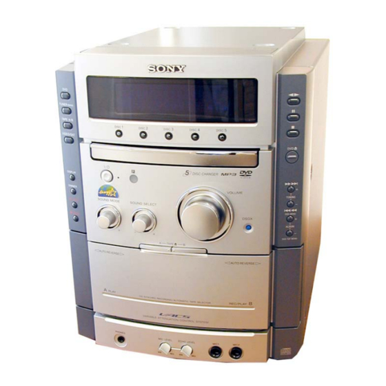
DISPLAY SIDE Hi-Fi COMPONENT SYSTEM
x
ao
u163
y
i
http://www.xiaoyu163.com
HCD-NXM4D
2 9
8
Model Name Using Similar Mechanism
DVD
DVD Mechanism Type
Section
Base Unit Name
Optical Pick-up Name
TAPE
Model Name Using Similar Mechanism
Q Q
Section
3
6 7
1 3
1 5
SPECIFICATIONS
S VIDEO OUT (4-pin/mini-DIN jack):
COMPONENT VIDEO OUT:
PHONES (stereo mini jack): accepts headphones of 8 ohms or
FRONT SPEAKER:
SURROUND SPEAKER:
CENTER SPEAKER :
SUB WOOFER SPEAKER: Use only the supplied speaker
co
.
9 4
2 8
l
NEW
CDM81A-DVBU60
DVBU60
DBU-3
HCD-CPX22
0 5
8
2 9
9 4
2 8
Y: 1 Vp-p, unbalanced,
Sync negative, C: 0.286 Vp-p, load
impedance 75 ohms
Y: 1 Vp-p, 75 ohms
PB, PR: 0.7 Vp-p, 75 ohms
more
Use only the supplied speaker
SS-NXM4D
Use only the supplied speaker
SS-RS400S
Use only the supplied speaker
SS-CT400S
SS-WG4D
– Continued on next page –
m
9 9
9 9
Advertisement
Table of Contents

Related Manuals for Sony HCD-NXM4D


Summary of Contents for Sony HCD-NXM4D
- Page 1 HCD-NXM4D 3 7 63 1515 0 SERVICE MANUAL Ver. 1.2 2005.05 • HCD-NXM4D is the Amplifier, DVD player, tape deck and tuner section in DHC-NXM4D. Model Name Using Similar Mechanism DVD Mechanism Type CDM81A-DVBU60 Section Base Unit Name DVBU60...
- Page 2 Tape deck section Recording system 4-track 2-channel stereo CAUTION Frequency response 50 – 13,000 Hz (±3 dB), using Sony Use of controls or adjustments or performance of procedures TYPE I cassette other than those specified herein may result in hazardous radiation exposure.
-
Page 3: Table Of Contents
HCD-NXM4D 3 7 63 1515 0 TABLE OF CONTENTS SERVICING NOTES 7-7. Printed Wiring Board – RF Board – ....... 36 ..........4 7-8. Schematic Diagram – RF Board – ........37 7-9. Printed Wiring Board – DVD Mechanism Board – ..38 GENERAL 7-10. -
Page 4: Servicing Notes
HCD-NXM4D SECTION 1 SERVICING NOTES 3 7 63 1515 0 • MODEL IDENTIFICATION NOTES ON HANDLING THE OPTICAL PICK-UP BLOCK – Back Panel – OR BASE UNIT The laser diode in the optical pick-up block may suffer electrostatic break-down because of the potential difference generated by the charged electrostatic load, etc. -
Page 5: General
HCD-NXM4D SECTION 2 GENERAL This section is extracted 3 7 63 1515 0 from instruction manual. LOCATING THE CONTROLS List of button locations and reference pages M a in unit BUTTON DESCRIP TIONS ALPHA BETICAL ORDER ?/1 (power) 1 A –... - Page 6 HCD-NXM4D This section is extracted from instruction manual. 3 7 63 1515 0 Rem ot e c ont rol ALPHABETICA L ORDER BUTTON DESCRIPTIONS ?/1 (power) 1 A – E F – Z nN (play) 6 ALBUM + 7...
-
Page 7: Disassembly
HCD-NXM4D SECTION 3 DISASSEMBLY 3 7 63 1515 0 • This set can be disassembled in the order shown below. 3-1. DISASSEMBLY FLOW 3-2.CASE (Page 8) 3-3.BACK PANEL (Page 8) 3-4.DVD SECTION (Page 9) 3-5.MAIN BOARD 3-10.VIDEO BOARD (Page 10) -
Page 8: Case
HCD-NXM4D 3 7 63 1515 0 Note: Follow the disassembly procedure in the numerical order given. 3-2. CASE 4 two screws (sumitite (B3)) 5 screw 7 CASE (sumitite (B3)) 2 three screws (CASE 3 TP2) 3 two screws (sumitite (B3)) -
Page 9: Dvd Section
HCD-NXM4D 3 7 63 1515 0 3-4. DVD SECTION 5 two screws (sumitite (B3)) 4 screw (+BVTP 3 X8 ) 6 DVD section 7 connector (CN102) 3 CNP372 2 CNP202 1 CNP200 L 13942296513 u163 http://www.xiaoyu163.com... -
Page 10: Main Board
HCD-NXM4D 3 7 63 1515 0 3-5. MAIN BOARD qs CNP110 qd CNP109 qa CNP112 4 MAIN board 0 connector (CN101) 1 two screws (sumitite (B3)) 3 connector (CN103) 5 CNP303 6 connector (CN108) 2 connector 8 connector (CN102) -
Page 11: Front Amp Boardm Sur Amp Board
HCD-NXM4D 3 7 63 1515 0 3-7. FRONT AMP BOARD, SUR AMP BOARD 5 screw (+BVTP 3 X8 ) 6 two screws 8 SUR AMP board (+BVTP 3 X8 ) 7 screw (+BVTP 3 X8 ) 9 connector (CN503) q;... -
Page 12: Tape Mechanism Deck
HCD-NXM4D 3 7 63 1515 0 3-8. TAPE MECHANISM DECK 4 two screws (+BVTP 2.6X8) 5 tape mechanism deck 3 two screws L 13942296513 (+P 2.6X3) 3-9. PANEL BOARD 5 screw (+BVTP 2.6X8) 3 screw (+BVTP 2.6X8) 4 bracket (main) 2 screw (+BVTP 2.6X8) -
Page 13: Video Board
HCD-NXM4D 3 7 63 1515 0 3-10. VIDEO BOARD 4 VIDEO board 2 screw (+BVTP 3 X8 ) 3 screw 1 CNP1101 (+BVTP 3 X8 ) 3-11. DMB07 BOARD, DVD MECHANISM DECK (CDM81A-DVBU60) L 13942296513 qs DVD mechanism deck... -
Page 14: Tray
HCD-NXM4D 3 7 63 1515 0 3-12. TRAY 2 two screws (+BTP 2.6X8) 1 two screws 3 bracket (+BTP 2.6X8) 5 tray L 13942296513 3-13. MOTOR BOARD, M761 (LD/ST MOTOR), M762 (BU U/D MOTOR) 1 screw (+BTP 2.6X8) 3 screw (+BTP 2.6X8) -
Page 15: Base Unit (Dvbu60)
HCD-NXM4D 3 7 63 1515 0 3-14. BASE UNIT (DVBU60) 1 two floating screws (+PTPWH2.6) 2 base unit (DVBU60) L 13942296513 3-15. RF BOARD 4 CNP101 3 RF board 1 screw (+BTP 2.6 X6 ) 2 screw (+BTP 2.6 X6 ) u163 http://www.xiaoyu163.com... -
Page 16: Optical Pick-Up (Dbu-3)
HCD-NXM4D 3 7 63 1515 0 3-16. OPTICAL PICK-UP (DBU-3) 5 step screw 0 insulator 6 step screw 8 optical pick-up qa insulator (DBU-3) 4 step screw 9 insulator 3 holder (DBU1) assy L 13942296513 1 screw 2 two screws (+BTP 2.6 X8 ) -
Page 17: Test Mode
HCD-NXM4D SECTION 4 TEST MODE 3 7 63 1515 0 [Change-over of AM Tuner Step between 9 kHz and 10 kHz] [GC Test Mode] • A step of AM channels can be changed over between 9 kHz • All fluorecent segments and LEDs are tested. - Page 18 HCD-NXM4D 3 7 63 1515 0 7. Press the [CD SYNC] button while “TAPE A” or “TAPE B” [DVD Repeat 5 Times Limit Release Mode] is selected, to perform AMS check. “EDG[ ]” is displayed. A number appears inside[ ].
-
Page 19: Mechanical Adjustments
HCD-NXM4D 3 7 63 1515 0 DVD OSD Test Mode • Example display [GENERAL DESCRIPTION] ### Syscon Diagnosis ### The Test Mode allows you to make diagnosis and adjustment easily using the remote commander and monitor TV. The instructions, Diag All Check diagnostic results, etc. - Page 20 HCD-NXM4D 3 7 63 1515 0 0-2-5. Region Model destination code is displayed. (2 digits number) Note: During adjustment of each disc, the measurement for disc type judg- ment is made. As automatic adjustment does not judge the disc type unlike conventional models, take care not to insert wrong type 0-3.
- Page 21 HCD-NXM4D 3 7 63 1515 0 1-3. DVD-DL (dual layer) In using the manual operation menu, take care of the following Press the [3] key on the remote commander and insert a DVD dual points. These commands do not provide protection, thus requiring layer disc following the message.
- Page 22 HCD-NXM4D 3 7 63 1515 0 Mirr Count : The number of times which mirror [1] LD : Turn on/off the laser. counts between disc surface and record [2] Focus : Search the focus and turn on the focus.
- Page 23 HCD-NXM4D 3 7 63 1515 0 [1] Focus Offset : Adjusts focus offset. [2] Focus Gain : Adjusts focus gain. EEPROM Data 2/2 CDRW DVDRW [3] TRK. Offset coares : Focus Gain Trk. Gain Adjusts tracking offset of the RF amp...
- Page 24 HCD-NXM4D 3 7 63 1515 0 2-9. SACD Water Mark Check (Not used) xxxxhxxm : The laser on total hours. Data below minutes are omitted. SACD Water Mark Check : Error number. : Error code. : Not used. PSP AMP •...
- Page 25 HCD-NXM4D 3 7 63 1515 0 aa: Initialization is completed or not. VERSION INFORMATION : Complete. On the Test Mode Menu screen, selecting [6] displays the ROM other number : Not complete. version and region code. bb: Operating status of mechanism deck at an error occurred.
-
Page 26: Electrical Adjustments
HCD-NXM4D SECTION 5 SECTION 6 3 7 63 1515 0 MECHANICAL ADJUSTMENTS ELECTRICAL ADJUSTMENTS Precaution DECK SECTION 0 dB=0.775 V 1. Clean the following parts with a denatured alcohol-moistened swab: 1. Demagnetize the record/playback head with a head record/playback heads pinch rollers demagnetizer. -
Page 27: Video Section
HCD-NXM4D 3 7 63 1515 0 2. Turn the adjustment screw and check output peaks. If the peaks VIDEO SECTION do not match for L-CH and R-CH, turn the adjustment screw so that outputs match within 1dB of peak. - Page 28 HCD-NXM4D 3 7 63 1515 0 RFMON Level Check Perform a RFMON level check before exchanging optical pick-up. Connection: oscilloscope JL005(RFMON) –RF board (side B) – – JL005 (RFMON) RFMON signal waveform VOLT/DIV: 200 mV TIME/DIV: 500 ns RFMON level L 13942296513 •...
-
Page 29: Diagrams
HCD-NXM4D SECTION 7 3 7 63 1515 0 DIAGRAMS 7-1. CIRCUIT BOARD LOCATION SUR AMP board MAIN board PANEL board DISC SW board VOL board switching regulator FRONT AMP board HP board L 13942296513 SW(2) board SW(1) board RELAY board... - Page 30 HCD-NXM4D 3 7 63 1515 0 For schematic diagrams. Note on Printed Wiring Boards: Note: • X : parts extracted from the component side. • All capacitors are in µF unless otherwise noted. (p: pF) • : Pattern from the side which enables seeing.
-
Page 31: Block Diagram - Dvd Dsp (1/2) Section
HCD-NXM4D 3 7 6 3 1 5 1 5 0 7-2. BLOCK DIAGRAM – DVD DSP (1/2) SECTION – OPTICAL PICK-UP IC509 BLOCK IC001 CD DECODER (DBU-3) DVD/CD RF AMP SERVO DSP DVDRFP RFAC 50 RFAC IC701 DVD DECODER... -
Page 32: Block Diagram - Dvd Dsp (2/2) Section
HCD-NXM4D 3 7 6 3 1 5 1 5 0 7-3. BLOCK DIAGRAM – DVD DSP (2/2) SECTION – IC302 LRCK D/A CONVERTER IC207 VOUT7 DM-L DVD SYSTEM PROCESSOR VOUT8 DM-R DVD DSP (1/2) SECTION 177-174 SDDATA0-SDDATA7, (Page 31) -
Page 33: Block Diagram - Tuner/Tape Deck Section
HCD-NXM4D 3 7 6 3 1 5 1 5 0 7-4. BLOCK DIAGRAM – TUNER/TAPE DECK SECTION – MAIN FL-OUT SECTION IC101 (Page 34) INPUT SELECT SWITCH SURR-L ELECTRICAL VOLUMEI MAIN SECTION (Page 34) MAIN L-OUT DPL-2 SECTION MD BUS... -
Page 34: Block Diagram - Main Section
HCD-NXM4D 3 7 6 3 1 5 1 5 0 7-5. BLOCK DIAGRAM – MAIN SECTION – CN201 TUNER/TAPE DECK ANALOG-IN-L ANALOG-IN-L ANALOG-IN-L SECTION Q102 DVD DSP(1/2) (Page 33) SECTION MUTE (Page 31) ANALOG-IN-R R-CH DM-L L OUT L-OUT... -
Page 35: Block Diagram - Amp Section
HCD-NXM4D 3 7 6 3 1 5 1 5 0 7-6. BLOCK DIAGRAM – AMP SECTION – IC501 POWER AMP TM502 CN501 FRONT Q505 R-CH OVER TUNER/TAPE R-CH LOAD DECK DETECT SECTION SUB WOOFER (Page 33) Q509 SPEAKER Q506... -
Page 36: Printed Wiring Board - Rf Board
HCD-NXM4D 3 7 6 3 1 5 1 5 0 7-7. PRINTED WIRING BOARD – RF SECTION – • See page 29 for Circuit Boards Location. (SIDE A) (SIDE B) RF BOARD RF BOARD OPTICAL PICK-UP BLOCK (DBU-3) DMB07... -
Page 37: Schematic Diagram - Rf Board
HCD-NXM4D 3 7 6 3 1 5 1 5 0 7-8. SCHEMATIC DIAGRAM – RF BOARD – • See page 63 for IC Block Diagram. • See page 62 for Waveforms. 1 3 9 4 2 2 9 6 5 1 3... -
Page 38: Printed Wiring Board - Dvd Mechanism Board
HCD-NXM4D 3 7 6 3 1 5 1 5 0 7-9. PRINTED WIRING BOARD – DVD MECHANISM BOARD – • See page 29 for Circuit Boards Location. MOTOR BOARD SENSOR BOARD M761 M762 1-861-240- (12) (LD/ST MOTOR) (BU U/D MOTOR) -
Page 39: Schematic Diagram - Dvd Mechanism Board
HCD-NXM4D 3 7 6 3 1 5 1 5 0 7-10. SCHEMATIC DIAGRAM – DVD MECHANISM BOARD – • See page 66 for IC Block Diagram. 1 3 9 4 2 2 9 6 5 1 3 (1/3) (Page 51) -
Page 40: Printed Wiring Board - Dmb07 Board (Side A)
HCD-NXM4D 3 7 6 3 1 5 1 5 0 7-11. PRINTED WIRING BOARD – DMB07 BOARD (Side A) – • See page 29 for Circuit Boards Location. MAIN VIDEO BOARD BOARD (Page50) (Page48) (SIDE A) DMB07 BOARD • Semiconductor Location Ref. -
Page 41: Printed Wiring Board - Dmb07 Board (Side B)
HCD-NXM4D 3 7 6 3 1 5 1 5 0 7-12. PRINTED WIRING BOARD – DMB07 BOARD (Side B) – • See page 29 for Circuit Boards Location. (SIDE B) DMB07 BOARD • Semiconductor Location Ref. No. Location D392... -
Page 42: Schematic Diagram - Dmb07 Board (1/6)
HCD-NXM4D 3 7 6 3 1 5 1 5 0 7-13. SCHEMATIC DIAGRAM – DMB07 (1/6) BOARD – • See page 64 for IC Block Diagram. • See page 62 for Waveforms. 1 3 9 4 2 2 9 6 5 1 3... -
Page 43: Schematic Diagram - Dmb07 Board (2/6)
HCD-NXM4D 3 7 6 3 1 5 1 5 0 7-14. SCHEMATIC DIAGRAM – DMB07 (2/6) BOARD – • See page 64 for IC Block Diagram. • See page 71 for IC Pin Function Description. • See page 62 for Waveforms. -
Page 44: Schematic Diagram - Dmb07 Board (3/6)
HCD-NXM4D 3 7 6 3 1 5 1 5 0 7-15. SCHEMATIC DIAGRAM – DMB07 (3/6) BOARD – • See page 65 for IC Block Diagram. • See page 74 for IC Pin Function Description. • See page 62 for Waveforms. -
Page 45: Schematic Diagram - Dmb07 Board (4/6)
HCD-NXM4D 3 7 6 3 1 5 1 5 0 7-16. SCHEMATIC DIAGRAM – DMB07 (4/6) BOARD – • See page 67 for IC Pin Function Description. • See page 62 for Waveforms. 1 3 9 4 2 2 9 6 5 1 3... -
Page 46: Schematic Diagram - Dmb07 Board (5/6)
HCD-NXM4D 3 7 6 3 1 5 1 5 0 7-17. SCHEMATIC DIAGRAM – DMB07 (5/6) BOARD – 1 3 9 4 2 2 9 6 5 1 3 w w w u 1 6 3 HCD-NXM4D http://www.xiaoyu163.com... -
Page 47: Schematic Diagram - Dmb07 Board (6/6)
HCD-NXM4D 3 7 6 3 1 5 1 5 0 7-18. SCHEMATIC DIAGRAM – DMB07 (6/6) BOARD – • See page 66 for IC Block Diagram. 1 3 9 4 2 2 9 6 5 1 3 w w w... -
Page 48: Printed Wiring Board - Video Board
HCD-NXM4D 3 7 6 3 1 5 1 5 0 7-19. PRINTED WIRING BOARD – VIDEO BOARD – • See page 29 for Circuit Boards Location. DMB07 BOARD (Page40) VIDEO BOARD 1 3 9 4 2 2 9 6 5 1 3... -
Page 49: Schematic Diagram - Video Board
HCD-NXM4D 3 7 6 3 1 5 1 5 0 7-20. SCHEMATIC DIAGRAM – VIDEO BOARD – • See page 62 for Waveforms. 1 3 9 4 2 2 9 6 5 1 3 w w w u 1 6 3 HCD-NXM4D http://www.xiaoyu163.com... -
Page 50: Printed Wiring Boards - Main Board
HCD-NXM4D 3 7 6 3 1 5 1 5 0 7-21. PRINTED WIRING BOARD – MAIN BOARD – • See page 29 for Circuit Boards Location. RELAY BOARD DMBO7 BOARD VOL BOARD DMBO7 BOARD (Page38) (page40) (Page56) (Page40) MAIN BOARD... -
Page 51: Schematic Diagram - Main Board (1/3)
HCD-NXM4D 3 7 6 3 1 5 1 5 0 7-22. SCHEMATIC DIAGRAM – MAIN BOARD (1/3) – 1 3 9 4 2 2 9 6 5 1 3 w w w u 1 6 3 HCD-NXM4D http://www.xiaoyu163.com... -
Page 52: Schematic Diagram - Main Board (2/3)
HCD-NXM4D 3 7 6 3 1 5 1 5 0 7-23. SCHEMATIC DIAGRAM – MAIN BOARD (2/3) – 1 3 9 4 2 2 9 6 5 1 3 w w w u 1 6 3 HCD-NXM4D http://www.xiaoyu163.com... -
Page 53: Schematic Diagram - Main Board (3/3)
HCD-NXM4D 3 7 6 3 1 5 1 5 0 7-24. SCHEMATIC DIAGRAM – MAIN BOARD (3/3)– • See page 76 for IC Pin Function Description. • See page 62 for Waveforms. 1 3 9 4 2 2 9 6 5 1 3... -
Page 54: Printed Wiring Boards - Panel Board
HCD-NXM4D 3 7 6 3 1 5 1 5 0 7-25. PRINTED WIRING BOARD – PANEL BOARD – • See page 29 for Circuit Boards Location. PANEL BOARD MAIN BOARD R1096 (Page 50) 1 3 9 4 2 2 9 6 5 1 3 •... -
Page 55: Schematic Diagram - Panel Board
HCD-NXM4D 3 7 6 3 1 5 1 5 0 7-26. SCHEMATIC DIAGRAM – PANEL BOARD – 1 3 9 4 2 2 9 6 5 1 3 (3/3) (Page 53) w w w u 1 6 3 HCD-NXM4D... -
Page 56: Printed Wiring Board - Disc Sw, Vol, Hp Board
HCD-NXM4D 3 7 6 3 1 5 1 5 0 7-27. PRINTED WIRING BOARD – DISC SW, VOL, HP BOARD – • See page 29 for Circuit Boards Location. HP BOARD DISC SW BOARD PHONES FRONT AMP BOARD (Page 58) -
Page 57: Schematic Diagram - Disc Sw, Vol, Hp Board
HCD-NXM4D 3 7 6 3 1 5 1 5 0 7-28. SCHEMATIC DIAGRAM – DISC SW, VOL, HP BOARD – • See page 66 for IC Block Diagram. 1 3 9 4 2 2 9 6 5 1 3... -
Page 58: Printed Wiring Board - Front Amp Board
HCD-NXM4D 3 7 6 3 1 5 1 5 0 7-29. PRINTED WIRING BOARD – FRONT AMP BOARD – • See page 29 for Circuit Boards Location. M962 MAIN BOARD DC FAN (Page50) • Semiconductor Location Ref. No. Location Ref. -
Page 59: Schematic Diagram - Front Amp Board
HCD-NXM4D 3 7 6 3 1 5 1 5 0 7-30. SCHEMATIC DIAGRAM – FRONT AMP BOARD – 1 3 9 4 2 2 9 6 5 1 3 w w w u 1 6 3 HCD-NXM4D http://www.xiaoyu163.com... -
Page 60: Printed Wiring Board - Suramp Board
HCD-NXM4D 3 7 6 3 1 5 1 5 0 7-31. PRINTED WIRING BOARD – SUR AMP BOARD – • See page 29 for Circuit Boards Location. SUR AMP BOARD • Semiconductor Location Ref. No. Location D511 D512 D601... -
Page 61: Schematic Diagram - Sur Amp Board
HCD-NXM4D 3 7 6 3 1 5 1 5 0 7-32. SCHEMATIC DIAGRAM – SUP AMP BOARD – 1 3 9 4 2 2 9 6 5 1 3 w w w u 1 6 3 HCD-NXM4D http://www.xiaoyu163.com... - Page 62 HCD-NXM4D 3 7 6 3 1 5 1 5 0 • WAVEFORMS – MAIN BOARD – – DMB07 BOARD – – RF BOARD – – VIDEO BOARD – IC1101 0 CY IN IC1101 wa Y OUT IC001 1 DVD RFP...
-
Page 63: Ic Block Diagram
HCD-NXM4D 3 7 63 1515 0 7-33. IC Block Diagram – RF Board – IC001 SP3723CAFOPM 64 63 62 61 60 59 55 54 53 52 FAST ATTACK INPUT OUTPUT HOLD FULL WAVE AGC CHARGE INHIBIT RECTIFER PUMP PROGRAMMABLE... - Page 64 HCD-NXM4D 3 7 63 1515 0 – DMB07 Board – IC509 CXD3068Q 59 58 57 56 55 54 53 52 51 50 49 48 47 46 45 44 43 42 41 DVDD2 ASYE DIGITAL ASYMMETRY CORRECTOR DIGITAL DOUT LRCK...
- Page 65 HCD-NXM4D 3 7 63 1515 0 – DMB07 Board – IC903 BR24C16F-WE2 1 A0 16 K bit EEPROM ARRAY 11 bit 8 bit 2 A1 ADDRESS SLAVE WORD DATA 11 bit DECODER ADDRESS REGISTER REGISTER START STOP 3 A2...
- Page 66 HCD-NXM4D 3 7 63 1515 0 – DMB07 Board – IC302 PCM1609KPTR 32 31 30 36 35 34 33 VCC3 FUNCTION AGND3 CONTROL VCC4 INTERFACE AGND4 SYSTEM SCKI CLOCK SCKO MANAGER VOUT8 AGND6 VCC5 LRCK AGND5 TEST 4X/8X ENHANCED...
- Page 67 HCD-NXM4D 3 7 63 1515 0 • IC Pin Function Descriptions • IC207 ZIVA5X-C2F (DVD SYSTEM PROCESSOR) (DMB07 BOARD) Pin No. Pin Name Description VDDP — Power supply terminal (+3.3V) (I/O signal) Address bus 3 to 11 HD15 to HD7...
- Page 68 HCD-NXM4D 3 7 63 1515 0 Pin No. Pin Name Description 88 to 95 MD20 to MD27 SDRAM data GND25 — Ground terminal (SDRAM I/O signal) MDQM3 Byte read /write mask signal 3 output VDD25 — Power supply terminal (+3.3V) (SDRAM I/O signal)
- Page 69 HCD-NXM4D 3 7 63 1515 0 Pin No. Pin Name Description LRCK LRCK signal output for audio BCK signal output for audio DATA0(DM) Audio data(Down Mix signal) output DATA1(FLR) Audio data(Front L/R signal) output VDDP — Power supply terminal (+3.3V) (I/O signal) GNDP —...
- Page 70 HCD-NXM4D 3 7 63 1515 0 Pin No. Pin Name Description Data output Data input TMS signal input TCK signal input RESET ZIVA reset input BUS CLK Not used — Ground terminal (inside core) — Power supply terminal (+1.8V) (inside core)
- Page 71 HCD-NXM4D 3 7 63 1515 0 • IC701 TMC57929PGF-RDP (DVD DECODER) (DBM07 Board) Pin No. Pin Name Description 1, 2 D5, D6 Two-way data bus with CXP973064-245R — Ground Two-way data bus with CXP973064-245R Address signal input from CXP973064-245R —...
- Page 72 HCD-NXM4D 3 7 63 1515 0 Pin No. Pin Name Description VDDS — Power supply (+5V) 59, 60 HA0, HA2 Not used (Pull up) — Ground (open) 62, 63 HCS0, HCS1 Not used — Power supply (+3.3V) DASP Not used...
- Page 73 HCD-NXM4D 3 7 63 1515 0 Pin No. Pin Name Description 128, 129 VCCA3, VCCA2 — Power supply (+3.3V) Signal output from the charge pump for phase comparator PDHVCC Middle point voltage input terminal for RF PLL Signal output from the charge pump for frequency comparator...
- Page 74 HCD-NXM4D 3 7 63 1515 0 • IC901 CXP973064-245R (MECHANISM CONTROLLER) (DBM07 Board) Pin No. Pin Name Description NO_USE Not used (open) SDEN Serial data enable signal output to SP3723CAFOPM DOCTRL/ Digital out on/off control signal output to CXD3068Q...
- Page 75 HCD-NXM4D 3 7 63 1515 0 Pin No. Pin Name Description CONTROL_1 Not used (open) GFS_DVD Guard frame sync signal input from TMC57929PGF-RDP MUTE_CD Muting on/off control signal output to CXD3068Q MUTE_2D Muting on/off control signal output to FAN8035L...
- Page 76 HCD-NXM4D 3 7 63 1515 0 • IC401 M3062CMEN-A01FPUO (SYSTEM CONTROL) (MAIN Board) Pin No. Pin Name Description M61530 CLK Serial clock output to M61530RP M61530 DATA Serial data output to M61530RP MIC IN MIC detect signal input SIRCS...
- Page 77 HCD-NXM4D 3 7 63 1515 0 Pin No. Pin Name Description TUNED IN Tuning detecton signal input from tuner unit ST-CE PLL chip enable signal output to tuner unit ST-DOUT PLL serial data output to tuner unit ST-DIN PLL serial data input from tuner unit...
-
Page 78: Exploded Views
HCD-NXM4D Ver. 1.2 SECTION 8 EXPLODED VIEWS 3 7 63 1515 0 NOTE: • -XX, -X mean standardized parts, so they may • Abbreviation The components identified by mark 0 or have some differences from the original one. : 120 V AC Area in E model dotted line with mark 0 are critical for •... -
Page 79: Front Panel Section
HCD-NXM4D Ver. 1.2 3 7 63 1515 0 8-2. FRONT PANEL SECTION not supplied not supplied L 13942296513 not supplied not supplied not supplied not supplied Ref. No. Part No. Description Remarks Ref. No. Part No. Description Remarks 4-252-535-11 KNOB (VOL) -
Page 80: Chassis Section
HCD-NXM4D 3 7 63 1515 0 8-3. CHASSIS SECTION CDM81A-DVBU60 not supplied not supplied M962 not supplied not supplied L 13942296513 not supplied The components identified by mark 0 or dotted line with mark 0 are critical for safety. -
Page 81: Dvd Mechanism Deck Section-1 (Cdm81A-Dvbu60)
HCD-NXM4D 3 7 63 1515 0 8-4. DVD MECHANISM DECK SECTION-1 (CDM81A-DVBU60) L 13942296513 Ref. No. Part No. Description Remarks Ref. No. Part No. Description Remarks 4-251-849-01 LEVER (SW2) X-4954-450-1 PULLEY (240) ASSY 4-251-991-01 SPRING (SW2), TORSION 3-053-844-01 YOKE... -
Page 82: Dvd Mechanism Deck Section-2 (Cdm81A-Dvbu60)
HCD-NXM4D 3 7 63 1515 0 8-5. DVD MECHANISM DECK SECTION-2 (CDM81A-DVBU60) not supplied not supplied M761 M762 L 13942296513 S771 not supplied not supplied Ref. No. Part No. Description Remarks Ref. No. Part No. Description Remarks 4-251-870-01 BELT (BU) -
Page 83: Dvd Mechanism Deck Section-3 (Cdm81A-Dvbu60)
HCD-NXM4D 3 7 63 1515 0 8-6. DVD MECHANISM DECK SECTION-3 (CDM81A-DVBU60) not supplied DVBU60 not supplied not supplied L 13942296513 S781 not supplied Ref. No. Part No. Description Remarks Ref. No. Part No. Description Remarks 4-985-672-01 SCREW (+PTPWHM2.6), FLOATING... -
Page 84: Base Unit (Dvbu60)
HCD-NXM4D 3 7 63 1515 0 8-7. BASE UNIT (DVBU60) L 13942296513 The components identified by mark 0 or dotted line with mark 0 are critical for safety. Replace only with part number specified. Ref. No. Part No. Description Remarks Ref. -
Page 85: Electrical Parts List
HCD-NXM4D SECTION 9 ELECTRICAL PARTS LIST DMB07 3 7 63 1515 0 DISC SW NOTE: • Due to standardization, replacements in the • COILS The components identified by mark 0 uH: µH parts list may be different from the parts... - Page 86 HCD-NXM4D DMB07 3 7 63 1515 0 Ref. No. Part No. Description Remarks Ref. No. Part No. Description Remarks C243 1-164-943-11 CERAMIC CHIP 0.01uF C323 1-107-820-11 CERAMIC CHIP 0.1uF C324 1-107-820-11 CERAMIC CHIP 0.1uF C244 1-164-943-11 CERAMIC CHIP 0.01uF...
- Page 87 HCD-NXM4D DMB07 3 7 63 1515 0 Ref. No. Part No. Description Remarks Ref. No. Part No. Description Remarks C552 1-216-295-91 SHORT CHIP C764 1-164-943-11 CERAMIC CHIP 0.01uF C553 1-164-940-11 CERAMIC CHIP 0.0033uF 10% C556 1-117-370-11 CERAMIC CHIP 10uF...
- Page 88 HCD-NXM4D DMB07 3 7 63 1515 0 Ref. No. Part No. Description Remarks Ref. No. Ref. No. Part No. Part No. Description Description Remarks Remarks D394 8-719-988-61 DIODE 1SS355TE-17 IC904 6-704-753-01 IC SN74AHC2G74HDCUR D500 8-719-988-61 DIODE 1SS355TE-17 IC906 6-700-407-01 IC SM8707GV-G-E2...
- Page 89 HCD-NXM4D DMB07 3 7 63 1515 0 Ref. No. Part No. Description Remarks Ref. No. Part No. Description Remarks R250 1-216-864-11 SHORT CHIP R353 1-216-864-11 SHORT CHIP R251 1-216-864-11 SHORT CHIP R362 1-216-833-11 METAL CHIP 1/10W R253 1-216-829-11 METAL CHIP 4.7K...
- Page 90 HCD-NXM4D DMB07 3 7 63 1515 0 Ref. No. Part No. Description Remarks Ref. No. Part No. Description Remarks R586 1-218-747-11 METAL CHIP 200K 0.5% 1/10W R765 1-216-837-11 METAL CHIP 1/10W R587 1-216-864-11 SHORT CHIP R767 1-216-841-11 METAL CHIP...
- Page 91 HCD-NXM4D DMB07 FRONT AMP 3 7 63 1515 0 Ref. No. Part No. Description Remarks Ref. No. Part No. Description Remarks R996 1-216-864-11 SHORT CHIP C538 1-131-992-91 CERAMIC CHIP 100000PF 35V (EA) R997 1-216-864-11 SHORT CHIP C539 1-131-992-91 CERAMIC CHIP...
- Page 92 HCD-NXM4D FRONT AMP 3 7 63 1515 0 Ref. No. Part No. Description Remarks Ref. No. Part No. Description Remarks 0 R524 < IC > 1-217-637-00 FUSIBLE 1/4W IC501 6-706-124-01 IC STK413-420 R525 1-249-677-31 CARBON 1.5K 1/2W IC850 6-703-610-01 IC RT8H015C-T112-1...
- Page 93 HCD-NXM4D FRONT AMP 3 7 63 1515 0 Ref. No. Part No. Description Remarks Ref. No. Part No. Description Remarks R582 1-216-841-11 METAL CHIP 1/10W C1064 1-162-964-11 CERAMIC CHIP 0.001uF R583 1-249-625-31 CARBON 1/2W (EA) C1066 1-162-949-11 CERAMIC CHIP...
- Page 94 HCD-NXM4D MAIN 3 7 63 1515 0 Ref. No. Part No. Description Remarks Ref. No. Part No. Description Remarks J1061 1-770-226-11 JACK (LARGE TYPE) (MIC 2) 1-124-261-00 ELECT 10uF J1063 1-750-032-11 JACK (DIA. 3.5) (PHONES) 1-124-261-00 ELECT 10uF < SHORT >...
- Page 95 HCD-NXM4D MAIN 3 7 63 1515 0 Ref. No. Part No. Description Remarks Ref. No. Part No. Description Remarks C146 1-162-969-11 CERAMIC CHIP 0.0068uF 10% C239 1-126-925-11 ELECT 470uF C147 1-162-927-11 CERAMIC CHIP 100PF C148 1-162-927-11 CERAMIC CHIP 100PF...
- Page 96 HCD-NXM4D MAIN 3 7 63 1515 0 Ref. No. Part No. Description Remarks Ref. No. Part No. Description Remarks C417 1-104-656-11 ELECT 2200uF 6.3V D395 8-719-988-61 DIODE 1SS355TE-17 C462 1-104-658-91 ELECT 100uF D396 8-719-988-61 DIODE 1SS355TE-17 C463 1-164-156-11 CERAMIC CHIP 0.1uF...
- Page 97 HCD-NXM4D MAIN 3 7 63 1515 0 Ref. No. Part No. Description Remarks Ref. No. Part No. Description Remarks JR119 1-216-864-11 SHORT CHIP Q101 8-729-120-28 TRANSISTOR 2SC1623-L5L6 Q102 6-550-889-01 TRANSISTOR 2SC5938-T112-1B JR120 1-216-864-11 SHORT CHIP JR121 1-216-864-11 SHORT CHIP...
- Page 98 HCD-NXM4D MAIN 3 7 63 1515 0 Ref. No. Part No. Description Remarks Ref. No. Part No. Description Remarks 1-216-825-11 METAL CHIP 2.2K 1/10W R121 1-216-861-11 METAL CHIP 2.2M 1/10W 1-216-833-11 METAL CHIP 1/10W 1-216-821-11 METAL CHIP 1/10W R122...
- Page 99 HCD-NXM4D MAIN 3 7 63 1515 0 Ref. No. Part No. Description Remarks Ref. No. Part No. Description Remarks R209 1-216-825-11 METAL CHIP 2.2K 1/10W R290 1-216-821-11 METAL CHIP 1/10W R210 1-216-825-11 METAL CHIP 2.2K 1/10W R291 1-216-825-11 METAL CHIP 2.2K...
- Page 100 HCD-NXM4D MAIN 3 7 63 1515 0 Ref. No. Part No. Description Remarks Ref. No. Part No. Description Remarks R379 1-216-833-11 METAL CHIP 1/10W R452 1-216-809-11 METAL CHIP 1/10W R380 1-216-833-11 METAL CHIP 1/10W R453 1-216-809-11 METAL CHIP 1/10W...
- Page 101 HCD-NXM4D MAIN MOTOR PANEL 3 7 63 1515 0 Ref. No. Part No. Description Remarks Ref. No. Part No. Description Remarks R958 1-216-809-11 METAL CHIP 1/10W < IC > R959 1-216-809-11 METAL CHIP 1/10W IC1020 6-705-745-01 IC M66005-0131AHPRB0T R969...
- Page 102 HCD-NXM4D PANEL RELAY 3 7 63 1515 0 Ref. No. Part No. Description Remarks Ref. No. Part No. Description Remarks S1030 1-762-875-21 SWITCH, KEYBOARD (DVD Z) C008 1-107-826-11 CERAMIC CHIP 0.1uF C009 1-107-826-11 CERAMIC CHIP 0.1uF S1031 1-762-875-21 SWITCH, KEYBOARD (X)
- Page 103 HCD-NXM4D SENSOR SUR AMP 3 7 63 1515 0 Ref. No. Part No. Description Remarks Ref. No. Part No. Description Remarks < TRANSISTOR > C604 1-126-947-11 ELECT 47uF C605 1-126-961-11 ELECT 2.2uF Q001 8-729-903-46 TRANSISTOR 2SB1132-P Q002 8-729-903-46 TRANSISTOR 2SB1132-P...
- Page 104 HCD-NXM4D SUR AMP SW (1) SW (2) VIDEO 3 7 63 1515 0 Ref. No. Part No. Description Remarks Ref. No. Part No. Description Remarks R613 1-216-841-11 METAL CHIP 1/10W C1106 1-126-960-11 ELECT C1107 1-126-960-11 ELECT R614 1-218-482-11 METAL CHIP...
- Page 105 HCD-NXM4D Ver. 1.2 VIDEO 3 7 63 1515 0 Ref. No. Part No. Description Remarks Ref. No. Part No. Description Remarks R1102 1-216-809-11 METAL CHIP 1/10W MISCELLANEOUS R1103 1-216-833-11 METAL CHIP 1/10W ************* R1104 1-218-285-11 METAL CHIP 1/10W R1105...
- Page 106 HCD-NXM4D 3 7 63 1515 0 MEMO L 13942296513 u163 http://www.xiaoyu163.com...
- Page 107 HCD-NXM4D 3 7 63 1515 0 E Model Australian Model SERVICE MANUAL Ver. 1.1 SUPPLEMENT-1 Subject: CDM81 DISASSEMBLY L 13942296513 u163 9-877-971-81 http://www.xiaoyu163.com...
- Page 108 HCD-NXM4D SECTION 1 3 7 63 1515 0 CDM81 DISASSEMBLY 1-1. DISASSEMBLY FLOW • This set can be disassembled in the order shown below. • The dotted square with arrow ( ) prompts you to move to the next job when all of the works within the dotted square ) are completed.
- Page 109 HCD-NXM4D 3 7 63 1515 0 1-2. GEAR (SUB TRAY 1), GEAR (SUB TRAY 2) PRECAUTION DURING GEAR (SUB TRAY 1/2) INSTALLATION 1 five screws (+PTPWH 2.6 × 8) Align the marks of the gears as shown in the illustration.
- Page 110 HCD-NXM4D 3 7 63 1515 0 1-4. STOCKER SECTION 2 stocker section 1 Rotate the gear (SS3) in the direction of the arrow. L 13942296513 1-5. CAM (STOCKER) PRECAUTION DURING CAM (STOCKER) INSTALLATION Before installing the cams (stocker), fix the gear (stocker 3) in...
- Page 111 HCD-NXM4D 3 7 63 1515 0 1-6. GEAR (STOCKER 3) PRECAUTION DURING GEAR (STOCKER 3) INSTALLATION 1 screw (+PTPWH 2.6 × 8) Be sure to align the rib of the gear (stocker 3) with the groove of the rotary encoder.
- Page 112 HCD-NXM4D 3 7 63 1515 0 1-8. GEAR (BU1) 1 belt (sub tray) PRECAUTION DURING GEAR (BU1) INSTALLATION 4 screw 2 screw Before re-assembling, slide the cam (BU) in the direction of (+PTPWH 2.6 × 8) (+PTPWH 2.6 × 8) the arrow.
- Page 113 HCD-NXM4D 3 7 63 1515 0 MEMO L 13942296513 u163 http://www.xiaoyu163.com...
- Page 114 HCD-NXM4D 3 7 63 1515 0 REVISION HISTORY Clicking the version allows you to jump to the revised page. Also, clicking the version at the upper right on the revised page allows you to jump to the next revised page.
Need help?
Do you have a question about the HCD-NXM4D and is the answer not in the manual?
Questions and answers