Table of Contents
Advertisement
QQ
3 7 63 1515 0
RX-SL100/RX-SL100RDS
TE
L 13942296513
I CONTENTS
To Service Personnel .......................................... 2
Front Panels ............................................................ 4
Rear Panels .......................................................... 5~6
Remote Control Panels ...................................... 6
Specifications .................................................... 7~10
Internal View ......................................................... 10
www
.
1 0 0 8 7 6
http://www.xiaoyu163.com
AV RECEIVER/AV AMPLIFIER
This manual has been provided for the use of authorized YAMAHA Retailers and their service personnel.
It has been assumed that basic service procedures inherent to the industry, and more specifically YAMAHA Products, are already
known and understood by the users, and have therefore not been restated.
WARNING:
Failure to follow appropriate service and safety procedures when servicing this product may result in personal
injury, destruction of expensive components, and failure of the product to perform as specified. For these reasons,
we advise all YAMAHA product owners that any service required should be performed by an authorized
YAMAHA Retailer or the appointed service representative.
IMPORTANT:
The presentation or sale of this manual to any individual or firm does not constitute authorization, certification or
recognition of any applicable technical capabilities, or establish a principle-agent relationship of any form.
The data provided is believed to be accurate and applicable to the unit(s) indicated on the cover. The research, engineering, and
service departments of YAMAHA are continually striving to improve YAMAHA products. Modifications are, therefore, inevitable
and specifications are subject to change without notice or obligation to retrofit. Should any discrepancy appear to exist, please
contact the distributor's Service Division.
WARNING:
Static discharges can destroy expensive components. Discharge any static electricity your body may have
accumulated by grounding yourself to the ground buss in the unit (heavy gauge black wires connect to this buss).
IMPORTANT:
Turn the unit OFF during disassembly and part replacement. Recheck all work before you apply power to the unit.
........... 11~13
........................................ 35
x
ao
u163
y
i
http://www.xiaoyu163.com
2 9
8
SERVICE MANUAL
IMPORTANT NOTICE
Q Q
3
6 7
1 3
1 5
Display Data ........................................................... 37
Ic Data ................................................................. 38~43
Block Diagram ................................................. 44~45
Pin Connection Diagram .................................... 46
Printed Circuit Board .................................. 47~57
SCHEMATIC DIAGRAM ........................................ 59~65
Parts List ........................................................... 67~81
Remote Control .............................................. 82~83
14~35
co
.
9 4
2 8
0 5
8
2 9
9 4
2 8
m
P.O.Box 1, Hamamatsu, Japan
9 9
9 9
36
Advertisement
Table of Contents

Related Manuals for Yamaha rx-sl100


Summary of Contents for Yamaha rx-sl100
-
Page 1: Service Manual
This manual has been provided for the use of authorized YAMAHA Retailers and their service personnel. It has been assumed that basic service procedures inherent to the industry, and more specifically YAMAHA Products, are already known and understood by the users, and have therefore not been restated. -
Page 2: To Service Personnel
RX-SL100/RX-SL100RDS 3 7 63 1515 0 I TO SERVICE PERSONNEL 1. Critical Components Information AC LEAKAGE Components having special characteristics are marked s and WALL EQUIPMENT TESTER OR OUTLET UNDER TEST EQUIVALENT must be replaced with parts having specifications equal to those originally installed. - Page 3 RX-SL100/RX-SL100RDS 3 7 63 1515 0 About Lead Free Solder / The P.C.B.s installed in this unit are soldered using the following solder. Component Side / Foil Side / DIGITAL P.C.B. Lead Solder / Lead Solder / INPUT P.C.B.
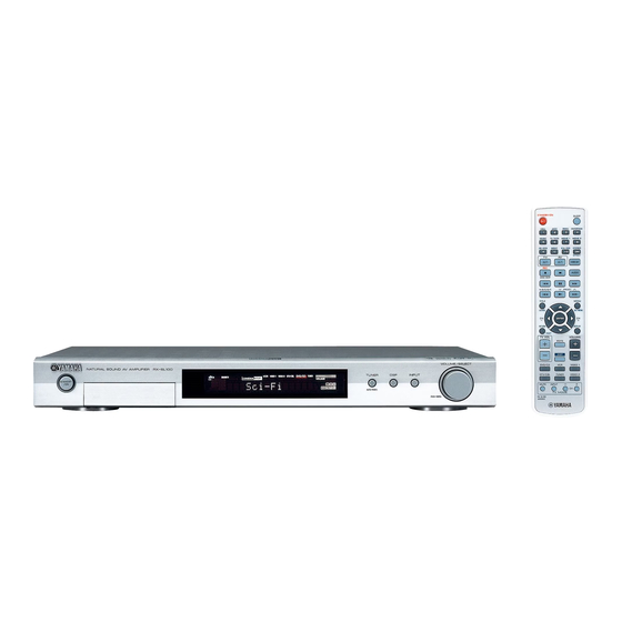
- Page 4 RX-SL100/RX-SL100RDS 3 7 63 1515 0 I FRONT PANELS RX-SL100 (U, C, A, L, R, T, K models) RX-SL100 (J model) L 13942296513 RX-SL100RDS (B, G models) u163 http://www.xiaoyu163.com...
- Page 5 RX-SL100/RX-SL100RDS 3 7 63 1515 0 I REAR PANELS RX-SL100 (U, C models) RX-SL100 (A model) RX-SL100 (L model) L 13942296513 RX-SL100 (R model) RX-SL100 (T model) RX-SL100 (K model) u163 http://www.xiaoyu163.com...
- Page 6 RX-SL100/RX-SL100RDS 3 7 63 1515 0 RX-SL100 (J model) RX-SL100RDS (B, G models) I REMOTE CONTROL PANELS RX-SL100 RX-SL100RDS L 13942296513 u163 http://www.xiaoyu163.com...
-
Page 7: Specifications
RX-SL100/RX-SL100RDS 3 7 63 1515 0 I SPECIFICATIONS I Audio Section Residual Noise (IHF-A network) FRONT L/R ........... 150 µV or less Minimum RMS Output Power (Power Amp. Section) Channel Separation (Vol -30 dB, Effect Off) (1 kHz) DVD/CD, etc. (Input 5.1 k-ohms shorted, 1 kHz/10 kHz) FRONT L/R ........ - Page 8 Power Consumption U, C models ............100 W A, B, G, L, R, T, K models ......... 100 W "SILENT CINEMA" is a trademark of YAMAHA CORPORATION. J model ............... 145 W Standby Power Consumption (reference data) U, C, R, J models ..........0.8 W A, L, T, K models ..........
- Page 9 RX-SL100/RX-SL100RDS 3 7 63 1515 0 • Set Menu Table L 13942296513 u163 ∞ http://www.xiaoyu163.com...
-
Page 10: Internal View
RX-SL100/RX-SL100RDS 3 7 63 1515 0 • The variable range of the parameter (Min/Max/Step) Unit Pro Logic II / IIx Parameter Unit DSP LEVEL -6 / +3 / 1 PLII / PLIIx PLII / PLIIx DELAY 1 / 99 / 1... -
Page 11: Disassembly Procedures
RX-SL100/RX-SL100RDS 3 7 63 1515 0 I DISASSEMBLY PROCEDURES * The description below uses RX-SL100RDS (G model) as a representative model. (Remove parts in the order as numbered.) Disconnect the power cable from the AC outlet. 1. Removal of Top Cover (Fig. 1) a. - Page 12 RX-SL100/RX-SL100RDS 3 7 63 1515 0 5. Removal of Rear Panel (Fig. 3) a. Remove 1 screw (7) and 3 screws (8). b. Remove the Rear Panel rearward. c. Remove CB4, CB6, CB51, CB404 and CB406. 6. Removal of INPUT (1) and POWER (9) P.C.B. (Fig. 4) a.
- Page 13 RX-SL100/RX-SL100RDS 3 7 63 1515 0 DIGITAL P.C.B. CB303 – POWER (1) P.C.B. CB5: DIGITAL P.C.B. CB303 – POWER (1) P.C.B. CB5: MFA18400 (18P 400mm) MFA18400 (18P 400mm) DIGITAL P.C.B. CB306 – INPUT (1) P.C.B. CB409: DIGITAL P.C.B. CB306 – INPUT (1) P.C.B. CB409:...
- Page 14 RX-SL100/RX-SL100RDS 3 7 63 1515 0 I SELF DIAGNOSIS FUNCTION (DIAG) There are 15 DIAG menu items, each of which has sub- menu items. Listed in the table below are menu items and sub-menu items. No DIAG menu sub-menu DSP THROUGH 1.
- Page 15 RX-SL100/RX-SL100RDS 3 7 63 1515 0 No DIAG menu sub-menu 11 IF STATUS 1. INSIDE STATUS 1 (5 Byte) 2. INSIDE STATUS 2 (3 Byte) 3. CHANNEL STATUS 1 (5 Byte) 4. CHANNEL STATUS 2 (5 Byte) 5. CHANNEL STATUS 3 (5 Byte) 6.
- Page 16 RX-SL100/RX-SL100RDS 3 7 63 1515 0 • Starting DIAG Press the “STANDBY/ON” key while simultaneously pressing the “INPUT” key. • Starting DIAG in the protection cancel mode If the protection function works and causes hindrance to trouble diagnosis, cancel the protection function as described below, and it will be possible to enter the DIAG mode.
- Page 17 RX-SL100/RX-SL100RDS 3 7 63 1515 0 • Display provided when DIAG started The FL display of the main unit displays the protection function history data and the version (1 alphabet) and the DIAG menu [sub-menu (ANALOG BYPASS) of DIAG menu No.1 DSP THROUGH] a few seconds later.
- Page 18 RX-SL100/RX-SL100RDS 3 7 63 1515 0 When there is a history of protection function due to excessive UCD amplifier temperature Version (1 alphabet) Voltage display in % Cause: The temperature of the UCD amplifier is excessive. Supplementary information: The abnormal voltage is displayed in % based on 5V as 500%.
- Page 19 RX-SL100/RX-SL100RDS 3 7 63 1515 0 • Operation procedure of DIAG menu and SUB-MENU Entering Menu Select Mode There are 15 MENU items, each of which has some SUB- MENU items. To select a DIAG MENU item or a SUB-MENU item, press the "TUNER"...
- Page 20 RX-SL100/RX-SL100RDS 3 7 63 1515 0 • Details of DIAG menu With full-bit output specified in some modes, it is possible to execute 0dBFS output without head margin in each channel. 1. DSP THROUGH Sub DSP of YSS938 is selected for MAIN L/R output.
- Page 21 RX-SL100/RX-SL100RDS 3 7 63 1515 0 YSS FULL BIT • The signal is output in digital full bit without including the head margin. The SWFR signal is output but not in digital full bit. Reference data INPUT: DVD ANALOG...
- Page 22 RX-SL100/RX-SL100RDS 3 7 63 1515 0 2. RAM THROUGH The main L/R signal is output from Sub DSP of YSS938. The CT, RC, RL/RR, FL/FR signals are output through Sub DSP - DRAM. RAM 0dB Reference data INPUT: DVD ANALOG...
- Page 23 RX-SL100/RX-SL100RDS 3 7 63 1515 0 3. PRO LOGIC PRO LOGIC I Reference data INPUT: DVD ANALOG SWFR: 50 Hz, Others: 1 kHz SPEAKER OUTPUT (1 kHz) SUBWOOFER Input level Volume FRONT L/R CENTER SURROUND L/R SURROUND BACK OUTPUT (50 Hz) - ∞...
- Page 24 RX-SL100/RX-SL100RDS 3 7 63 1515 0 Neo:6 Reference data INPUT: DVD ANALOG SWFR: 50 Hz, Others: 1 kHz SPEAKER OUTPUT (1 kHz) SUBWOOFER Input level Volume FRONT L/R CENTER SURROUND L/R SURROUND BACK OUTPUT (50 Hz) - ∞ - ∞...
- Page 25 RX-SL100/RX-SL100RDS 3 7 63 1515 0 4. SPEAKERS SET The input signal is automatically identified and switched in the priority order of dts → DOLBY DIGITAL → AAC → PCM AUDIO → Analog (A/D) according to the signal detection.
- Page 26 RX-SL100/RX-SL100RDS 3 7 63 1515 0 Reference data INPUT: DVD ANALOG (Both ch) SPEAKER OUTPUT (1 kHz) SUBWOOFER Sub-menu Input level Volume FRONT L/R CENTER SURROUND L/R SURROUND BACK OUTPUT (50 Hz) - ∞ - ∞ - ∞ - ∞...
- Page 27 RX-SL100/RX-SL100RDS 3 7 63 1515 0 6. OTHER INPUT The signal input through the 6CH INPUT terminals is output. (Not applied to this model.) EXTERNAL DECODER 7. DISPLAY CHECK This program is used to check the FL display section. The display condition varies as shown below according to the sub-menu operation.
- Page 28 RX-SL100/RX-SL100RDS 3 7 63 1515 0 8. MANUAL TEST The noise generator built into the DSP outputs the test noise through the channels specified by the sub-menu. The noise frequency for LFE is 35 to 250 Hz. Other than that, the center frequency is 800 Hz.
- Page 29 RX-SL100/RX-SL100RDS 3 7 63 1515 0 • PRESET STATIONS / STATION FM FACTORY PRESET DATA (MHz) STATION AM FACTORY PRESET DATA (kHz) PAGE NO. U, C R, T, K, A, B, G, L PAGE NO. U, C, R, T, K A, B, G, L 87.5...
- Page 30 RX-SL100/RX-SL100RDS 3 7 63 1515 0 IMP SW (Impedance) Not applied to this model. K0/K1 (Panel key of main unit) A/D of the key fails to function properly when the standard value is deviated. In this case, check the constant of partial pressure resistor, solder condition, etc.
- Page 31 RX-SL100/RX-SL100RDS 3 7 63 1515 0 11. IF STATUS (Input function status) Using the sub-menu, the status data is displayed one after another in the hexadecimal notation. During signal processing, the status before execution of this menu is maintained.
- Page 32 RX-SL100/RX-SL100RDS 3 7 63 1515 0 <5th byte> Signal processing status information *2: With digital signals other than 32 kHz, 44.1 kHz and 48 kHz, through processing method is used for reproducible signals. bit7 MUTE request bit3 – bit6 Red dts flashing bit2 Through &...
- Page 33 RX-SL100/RX-SL100RDS 3 7 63 1515 0 12. DSP RAM CHECK This menu is used to self-diagnose whether or not the bus connection for the YSS938 and the external RAM is made properly. During signal processing, the status before execution of this menu is maintained.
- Page 34 RX-SL100/RX-SL100RDS 3 7 63 1515 0 14. SOFT SW This menu is used to switch the function settings on P.C.B. through the software so as to activate the product. The protection function follows the P.C.B. settings. When connected to AC or in the maker preset state, the unit is initialized to the P.C.
- Page 35 RX-SL100/RX-SL100RDS 3 7 63 1515 0 15. MICROPROCESSOR INFORMATION The version, checksum and the port specified by the microprocessor are displayed. The signal is processed using EFFECT OFF. The checksum is obtained by adding the data at every 8 bits for each program area and expressing the result as a 4-figure hexadecimal data.
-
Page 36: Amp Adjustment
RX-SL100/RX-SL100RDS 3 7 63 1515 0 I AMP ADJUSTMENT Condition • Start adjustment 5 sec or more after the power is turned • Headphones are not plugged in. • No input signal. Equipment required Screwdriver with angled shank as shown below... - Page 37 RX-SL100/RX-SL100RDS 3 7 6 3 1 5 1 5 0 I DISPLAY DATA G V101 : HNA-16SM08T (WB569700) G ANODE CONNECTION 13G~1G PATTERN AREA 5-11 G PIN CONNECTION PIN NO. 28 27 26 25 24 23 22 21 20 19 18 17 16 15 14 13 12 11 10 9 CONNECTION NP NP NP NP NP NP NP NP NX 15G 14G 13G 12G 11G 10G 9G 8G 7G 6G 5G 4G 3G 2G 1G NP NP F1 F1 PIN NO.
- Page 38 RX-SL100/RX-SL100RDS 3 7 6 3 1 5 1 5 0 I IC DATA IC304: YSS938 (DIGITAL P.C.B) IC304: YSS938 (DIGITAL P.C.B) Name Function Crystal oscillator connecting terminal Crystal oscillator connecting terminal (24.576MHz) SELI1 Built-in selector input 1 (Unconnected) (AXD)
- Page 39 RX-SL100/RX-SL100RDS 3 7 6 3 1 5 1 5 0 IC304: YSS938 (DIGITAL P.C.B) IC304: YSS938 (DIGITAL P.C.B) Name Function Name Function SDWCKI1 Word clock input terminal for SDIB, SDOB interface (Unconnected) (WCKG) RAMA5 Sub DSP: External memory address terminal 5...
- Page 40 RX-SL100/RX-SL100RDS 3 7 6 3 1 5 1 5 0 IC307: M30805SGP (DIGITAL P.C.B) IC307: M30805SGP (DIGITAL P.C.B) 16bit µ-COM (Main CPU) 16bit µ-COM (Main CPU) Pin Pin Name Type Function Name Detail Of Function TxD4 S-OUT CS493x TxD...
- Page 41 RX-SL100/RX-SL100RDS 3 7 6 3 1 5 1 5 0 IC307: M30805SGP (DIGITAL P.C.B) IC307: M30805SGP (DIGITAL P.C.B) 16bit µ-COM (Main CPU) 16bit µ-COM (Main CPU) Pin Pin Name Type Function Name Detail Of Function Pin Pin Name Type...
- Page 42 RX-SL100/RX-SL100RDS 3 7 6 3 1 5 1 5 0 IC317: YGV619 (DIGITAL P.C.B) IC317: YGV619 (DIGITAL P.C.B) Video Display Video Display Name Function Name Function AVSS1 Ground for Analog Logic of PLLDCK (GND) CPU Data Bus (Unconnected) AVDD1 Power Supply for Analog Logic of PLLDCK (+3.3 V)
- Page 43 RX-SL100/RX-SL100RDS 3 7 6 3 1 5 1 5 0 IC317: YGV619 (DIGITAL P.C.B) IC317: YGV619 (DIGITAL P.C.B) Video Display Video Display Name Function Name Function /RAS SDRAM Row Address Strobe DRO0 Digital R Output (Unconnected) /SCS Chip Select for SDRAM Access...
- Page 44 RX-SL100/RX-SL100RDS 3 7 6 3 1 5 1 5 0 I BLOCK DIAGRAM (U, C, A, L, R, T, K, J models) • See page 64 → IC402 FL/FR (DSP THROUGH) SCHEMATIC DIAGRAM SELECTOR MUTE [Front] POWER (5) IC419 TC74H4053AF •...
- Page 45 RX-SL100/RX-SL100RDS 3 7 6 3 1 5 1 5 0 I BLOCK DIAGRAM (B, G models) • See page 64 → IC402 FL/FR (DSP THROUGH) SCHEMATIC DIAGRAM SELECTOR MUTE POWER (5) [Front] IC419 TC74H4053AF • See page 62 →...
- Page 46 RX-SL100/RX-SL100RDS 3 7 6 3 1 5 1 5 0 I PIN CONNECTION DIAGRAM • ICs • Diodes 1N4002S 1SR154 MA8110-H SB01-05Q µPC29M33T-E1 NJM78M12FA NJM78M05DL1A 0NJM79M12DL1A NJM79M05DL1A PQ05RA1 1SS355 MA8120-M 1SS380 MA8270-M MA8047-M RB051L-40 Anode MA8056-M RB501V-40 MA8062-H UDZ5.1B MA8062-M UDZ7.5B...
- Page 47 RX-SL100/RX-SL100RDS 3 7 6 3 1 5 1 5 0 I PRINTED CIRCUIT BOARD (Foil side) DIGITAL P. C. B. (Lead Type Device) DIGITAL P. C. B. (Surface Mount Device) B, G models only INPUT (1) POWER (12) INPUT (2)
- Page 48 RX-SL100/RX-SL100RDS 3 7 6 3 1 5 1 5 0 I PRINTED CIRCUIT BOARD (Foil side) INPUT (1) P. C. B. (Lead Type Device) INPUT (2) P. C. B. (Lead Type Device) U, C, A, L, R, T, K, J...
- Page 49 RX-SL100/RX-SL100RDS 3 7 6 3 1 5 1 5 0 I PRINTED CIRCUIT BOARD (Foil side) INPUT (1) P. C. B. (Surface Mount Device) INPUT (2) P. C. B. (Surface Mount Device) 1 3 9 4 2 2 9 6 5 1 3 Ref.
- Page 50 RX-SL100/RX-SL100RDS 3 7 6 3 1 5 1 5 0 I PRINTED CIRCUIT BOARD (Foil side) POWER (1) MAIN (1) P. C. B. (Lead Type Device) MAIN (4) UCD-B UCDG UCD+B ENABLE UCH2OUT AGND_CH1 UCDG_CH2 UCH1IN UCH1OUT AGND_CH1 UCDG_CH1...
- Page 51 RX-SL100/RX-SL100RDS 3 7 6 3 1 5 1 5 0 I PRINTED CIRCUIT BOARD (Foil side) POWER (1) MAIN (3) P. C. B. (Lead Type Device) MAIN (4) UCD-B UCDG UCD_TH UCD+B ENABLE UCH6OUT DGND UCDG_CH6 UCH5IN UCDG_CH6 AGND_CH5...
- Page 52 RX-SL100/RX-SL100RDS 3 7 6 3 1 5 1 5 0 I PRINTED CIRCUIT BOARD (Foil side) POWER (1) P. C. B. (Lead Type Device) DIGITAL S3.3BK FROM_RST S3.3V S5BK SGND RESET PW_DN POW_RY MAIN TRANSFORMER AC_PRT DC_PRT -27V STBY_CTRL 1 3 9 4 2 2 9 6 5 1 3 +10.6V...
- Page 53 RX-SL100/RX-SL100RDS 3 7 6 3 1 5 1 5 0 I PRINTED CIRCUIT BOARD (Foil side) POWER (1) P. C. B. (Surface Mount Device) 1 3 9 4 2 2 9 6 5 1 3 POWER (3) P. C. B.
- Page 54 RX-SL100/RX-SL100RDS 3 7 6 3 1 5 1 5 0 I PRINTED CIRCUIT BOARD (Foil side) POWER (4) P. C. B. (Lead Type Device) DIGITAL INPUT (1) VOLUME / SELECT INPUT TUNER 1 3 9 4 2 2 9 6 5 1 3 POWER (5) P.
- Page 55 RX-SL100/RX-SL100RDS 3 7 6 3 1 5 1 5 0 I PRINTED CIRCUIT BOARD (Foil side) POWER (4) P. C. B. (Surface Mount Device) 49 48 16 17 1 3 9 4 2 2 9 6 5 1 3 POWER (5) P.
- Page 56 RX-SL100/RX-SL100RDS 3 7 6 3 1 5 1 5 0 I PRINTED CIRCUIT BOARD (Foil side) POWER (9) P. C. B. (Lead Type Device) POWER (10) P. C. B. (Lead Type Device) B, G models only INPUT (1) INPUT (1)
- Page 57 RX-SL100/RX-SL100RDS 3 7 6 3 1 5 1 5 0 I PRINTED CIRCUIT BOARD (Foil side) POWER (9) P. C. B. (Surface Mount Device) POWER (10) P. C. B. (Surface Mount Device) Ref. No. Location D301 D302 D303 IC261...
- Page 58 RX-SL100/RX-SL100RDS SCHEMATIC DIAGRAM (DIGITAL) Page 63 Page 64 Page 64 Page 60 Page 65 to POWER (1) to POWER (5) to POWER (4) to INPUT (1) to POWER (12) IC301: CY62256LL-70SNCT Static RAM RGB ENCODER INPUT BUFFER 512x512 ARRAY...
- Page 59 RX-SL100/RX-SL100RDS SCHEMATIC DIAGRAM (INPUT 1/2) # All voltages are measured with a 10MΩ/V DC electronic volt meter. Page 59 Page 64 Page 59 Page 65 Page 65 to DIGITAL to POWER (4) to DIGITAL # Components having special characteristics are marked s and must be...
- Page 60 RX-SL100/RX-SL100RDS SCHEMATIC DIAGRAM (INPUT 2/2) DIGITAL INPUT IC551, 552: TC74HCU04AFEL Hex Inverters # All voltages are measured with a 10MΩ/V DC electronic volt meter. # Components having special characteristics are marked s and must be replaced with parts having specifications equal to those originally installed.
- Page 61 RX-SL100/RX-SL100RDS SCHEMATIC DIAGRAM (MAIN) Page 63 Page 63 Page 63 Page 63 Page 63 Page 63 IC691~693: NJM2068MD-TE2 to POWER (3) to POWER (1) to POWER (3) to POWER (1) to POWER (3) to POWER (1) Dual OP-Amp. –IN –...
- Page 62 RX-SL100/RX-SL100RDS SCHEMATIC DIAGRAM (POWER 1/3) SURROUND L SURROUND BACK CENTER FRONT L 11.5 42.2 11.9 42.2 11.9 12.3 12.3 42.3 -41.9 13.0 AC 61.7 13.0 12.3 -28.3 -27.7 -40.5 -40.5 12.8 10.8 12.6 15.5 12.6 AC 13.5 11.4 11.9 12.6...
- Page 63 RX-SL100/RX-SL100RDS SCHEMATIC DIAGRAM (POWER 2/3) FL DISPLAY STANDBY/ON -23.6 -25.7 -23.7 -25.6 -25.7 -27.6 -20.3 -23.8 -25.7 -21.7 -23.7 -27.6 -23.6 -27.8 -23.7 FL DRIVER -23.8 -27.6 -19.8 -23.8 -23.8 -23.7 -23.7 -19.9 -20.0 -20.0 -27.6 -18.1 -25.7 -25.7 -18.0...
- Page 64 RX-SL100/RX-SL100RDS SCHEMATIC DIAGRAM (POWER 3/3) Page 59 to DIGITAL 10.8 10.8 10.7 x: NOT USED O: USED / APPLICABLE 10.8 10.8 IC303~304: BA7613N Video Signal Selector MUTE 6dB Amp. 75ohm Driver Logic IC301: BD3842FS-E2 Function Switch IC261: TC74HC4051AFEL IC281: LA7108M...
-
Page 65: Parts List
RX-SL100/RX-SL100RDS PARTS LIST 3 7 63 1515 0 I ELECTRICAL PARTS I WARNING Components having special characteristics are marked s and must be replaced with parts having specifications equal to those originally installed. ABBREVIATIONS IN THIS LIST ARE AS FOLLOWS: C.A.EL.CHP... - Page 66 RX-SL100/RX-SL100RDS 3 7 63 1515 0 P.C.B. DIGITAL L 13942296513 u163 ✻ New Parts http://www.xiaoyu163.com...
- Page 67 RX-SL100/RX-SL100RDS 3 7 63 1515 0 P.C.B. DIGITAL & P.C.B. INPUT L 13942296513 u163 ✻ New Parts http://www.xiaoyu163.com...
- Page 68 RX-SL100/RX-SL100RDS 3 7 63 1515 0 P.C.B. INPUT L 13942296513 u163 ✻ New Parts http://www.xiaoyu163.com...
- Page 69 RX-SL100/RX-SL100RDS 3 7 63 1515 0 P.C.B. INPUT L 13942296513 u163 ✻ New Parts http://www.xiaoyu163.com...
- Page 70 RX-SL100/RX-SL100RDS 3 7 63 1515 0 P.C.B. INPUT L 13942296513 u163 ✻ New Parts http://www.xiaoyu163.com...
- Page 71 RX-SL100/RX-SL100RDS 3 7 63 1515 0 P.C.B. MAIN L 13942296513 u163 ✻ New Parts http://www.xiaoyu163.com...
- Page 72 RX-SL100/RX-SL100RDS 3 7 63 1515 0 P.C.B. MAIN L 13942296513 u163 ✻ New Parts http://www.xiaoyu163.com...
- Page 73 RX-SL100/RX-SL100RDS 3 7 63 1515 0 P.C.B. POWER L 13942296513 u163 ✻ New Parts http://www.xiaoyu163.com...
- Page 74 RX-SL100/RX-SL100RDS 3 7 63 1515 0 P.C.B. POWER L 13942296513 u163 ✻ New Parts http://www.xiaoyu163.com...
- Page 75 RX-SL100/RX-SL100RDS 3 7 63 1515 0 P.C.B. POWER L 13942296513 u163 ✻ New Parts http://www.xiaoyu163.com...
- Page 76 RX-SL100/RX-SL100RDS 3 7 63 1515 0 P.C.B. POWER L 13942296513 u163 ✻ New Parts http://www.xiaoyu163.com...
- Page 77 RX-SL100/RX-SL100RDS 3 7 6 3 1 5 1 5 0 P.C.B. POWER & Chip Parts Chip Parts 1 3 9 4 2 2 9 6 5 1 3 w w w u 1 6 3 ✻ New Parts ✻ New Parts...
- Page 78 RX-SL100/RX-SL100RDS 3 7 6 3 1 5 1 5 0 I EXPLODED VIEW I MECHANICAL PARTS B, G models 8 (2) 1-20 8 (6) 8 (12) 8 (9) 1-20 1-13 1-40 1-12 1-13 1-11 1-20 1-10 1-11 8 (4)
- Page 79 RX-SL100/RX-SL100RDS 3 7 63 1515 0 L 13942296513 u163 ✻ New Parts http://www.xiaoyu163.com...
- Page 80 RX-SL100/RX-SL100RDS 3 7 63 1515 0 I REMOTE CONTROL P0D2 P1A2 3.0V 47µF P0D3 P0D1 P1B0/INT P0D0 P0E0 P0C3 P0E1 P0C2 2Ω (1/4W) P0E2 P0C1 MIE554A2 P0E3 P0C0 AV STANDBY/ON SKIP (–) DOWN VOLUME (+) TV MUTE P0B3 VIDEO 2 TV STANDBY/ON SEARCH (+) 27Ω...
- Page 81 RX-SL100/RX-SL100RDS 3 7 63 1515 0 RX-SL100 RX-SL100RDS Function TUNER STANDBY/ON 7A-1F – SLEEP 7A-57 – 7A-88 7A-E5 7A-89 7A-E6 7A-8A 7A-E7 7A-8B 7A-E8 7A-8C 7A-E9 7A-8D 7A-EA 7A-8E 7A-EB 7A-8F 7A-EC 7A-90 – 7A-95 – 7A-97 – ENTER 7A-56 –...
- Page 82 3 7 63 1515 0 RX-SL100/RX-SL100RDS L 13942296513 u163 http://www.xiaoyu163.com...
Need help?
Do you have a question about the rx-sl100 and is the answer not in the manual?
Questions and answers