Table of Contents
Advertisement
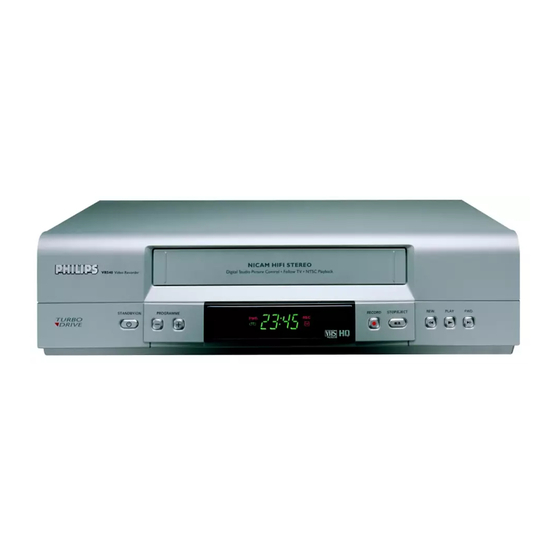
Video Cassette Recorder
Service
Service
Service
Service Manual
Contents
Chapter
Sec. 1:
Adjustment Procedure
Schematic Diagrams and CBA's
Exploded Views
Mechanical and Electrical Parts Lists
Sec. 2: Standard Maintenance
Mechanism Alignment Procedures
Disassembly / Assembly of Mechanism
Deck Exploded Views
Safety regulations require that the set be restored to its original
condition and that parts which are identical with those specified
be used.
Published by BK 2003 Video Service Department
VR540
Survey of versions:
/02
PAL B/G, VPS/PDC
/07
PAL I, Ireland
/16
PAL B/G, Spain
/39
SECAM L,L' & PAL B/G, I
/58
PAL/SECAM B/G, D/K
Printed in Japan
c Copyright reserved
/02/07/16
Subject to modification
GB
3103 785 22140
Advertisement
Chapters
Table of Contents

Related Manuals for Philips VR-540-02


Summary of Contents for Philips VR-540-02
- Page 1 Video Cassette Recorder Service Service VR540 /02/07/16 Service Service Manual Contents Survey of versions: PAL B/G, VPS/PDC Chapter PAL I, Ireland PAL B/G, Spain Sec. 1: Adjustment Procedure SECAM L,L' & PAL B/G, I Schematic Diagrams and CBA's Exploded Views PAL/SECAM B/G, D/K Mechanical and Electrical Parts Lists Sec.
-
Page 2: Table Of Contents
MAIN SECTION VIDEO CASSETTE RECORDER Sec. 1: Main Section I Adjustment Procedures I Schematic Diagrams and CBA’s I Exploded Views I Mechanical and Electrical Parts List TABLE OF CONTENTS IMPORTANT SAFETY PRECAUTIONS ............1-1-1 STANDARD NOTES FOR SERVICING. -
Page 3: Important Safety Precautions
IMPORTANT SAFETY PRECAUTIONS Product Safety Notice I. Also check areas surrounding repaired locations. J. Use care that foreign objects (screws, solder drop- Some electrical and mechanical parts have special lets, etc.) do not remain inside the set. safety-related characteristics which are often not evi- K. - Page 4 Safety Check after Servicing Chassis or Secondary Conductor Examine the area surrounding the repaired location for damage or deterioration. Observe that screws, parts, and wires have been returned to their original posi- Primary Circuit Terminals tions. Afterwards, do the following tests and confirm the specified values to verify compliance with safety standards.
-
Page 5: Standard Notes For Servicing
STANDARD NOTES FOR SERVICING Circuit Board Indications How to Remove / Install Flat Pack-IC a. The output pin of the 3 pin Regulator ICs is indi- 1. Removal cated as shown. With Hot-Air Flat Pack-IC Desoldering Machine:. (1) Prepare the hot-air flat pack-IC desoldering Top View Bottom View machine, then apply hot air to the Flat Pack-IC... - Page 6 With Soldering Iron: (4) Bottom of the flat pack-IC is fixed with glue to the CBA; when removing entire flat pack-IC, first apply (1) Using desoldering braid, remove the solder from all soldering iron to center of the flat pack-IC and heat pins of the flat pack-IC.
- Page 7 2. Installation Instructions for Handling Semi-conductors (1) Using desoldering braid, remove the solder from the foil of each pin of the flat pack-IC on the CBA Electrostatic breakdown of the semi-conductors may so you can install a replacement flat pack-IC more occur due to a potential difference caused by electro- easily.
-
Page 8: Function Indicator Symbols
FUNCTION INDICATOR SYMBOLS Note: The following symbols will appear on the indicator panel to indicate the current mode or operation of the VCR. On-screen modes will also be momentarily displayed on the tv screen when you press the operation buttons. Display panel "... -
Page 9: Preparation For Servicing
PREPARATION FOR SERVICING How to Enter the Service Mode About Optical Sensors Caution: An optical sensor system is used for the Tape Start and End Sensors on this equipment. Carefully read and follow the instructions below. Otherwise the unit may operate erratically. What to do for preparation Insert a tape into the Deck Mechanism Assembly and press the PLAY button. -
Page 10: Operating Controls And Functions
VCR. Buttons with TV feature To call up additional TV functions. STANDBY/ON y y To switch VCR or Philips TV on or off, interrupt menu function. STATUS/EXIT To access or remove the VCR’s on-screen status display. To exit on-screen menus. Or, to access or remove a status display or menu of Philips TV. - Page 11 Front of the device STANDBY/ON PROGRAMME RECORD STOP/EJECT PLAY STANDBY/ON To switch off or on, interrupt a function. PROGRAMME+ PROGRAMME- To select the programme number. During normal or slow motion playback, press to adjust the tracking. RECORD To record the TV channel selected at this moments. When tape playback is stopped, press to fast forward the tape at hight speed.
-
Page 12: Signal Name Abbreviations
SIGNAL NAME ABBREVIATIONS Signal Name Function Signal Name Function C-SYNC Composite Synchronized Pulse SCART 1 8Pin Output Control 8POUT-1 CLKSEL Clock Select (GND) Signal SECAM or MESECAM Chroma SCART 2 8Pin Output Control 8POUT-2 COLOR-IN Video Input Signal at Super Signal Impose A-COM... - Page 13 Signal Name Function Signal Name Function KEY-1 Key Scan Input Signal 1 Supply Reel S-REEL Rotation Signal KEY-2 Key Scan Input Signal 2 SC2-IN Input Signal from Pin 8 of SCART2 Deck Mode Position Detector LD-SW Signal Tape Start Position Detector ST-S Signal LINE MUTE...
-
Page 14: Cabinet Disassembly Instructions
CABINET DISASSEMBLY INSTRUCTIONS 1. Disassembly Flowchart (1): Identification (location) No. of parts in the figures (2): Name of the part This flowchart indicates the disassembly steps to gain (3): Figure Number for reference access to item(s) to be serviced. When reassembling, (4): Identification of parts to be removed, unhooked, follow the steps in reverse order. - Page 15 (S-2) (S-1) (S-3) (S-1) (S-2) (S-2) (S-4) [3]VCR Chassis Unit (S-3) (S-2) [1] Top Case (S-1) Fig. 1 (L-2) (L-2) Fig. 3 [4] Jack CBA (S-5) [2] Front Desolder Assembly (L-1) Fig. 2 Fig. 4 1-7-2 HE470DC...
- Page 16 [7] Cylinder Shield Cylinder Assembly FE Head (S-7) SW507 AC Head LD-SW Assembly [6] Main CBA [5] Deck Assembly [5] Deck Assembly Cam Gear [6] Main CBA Hole Shaft (S-6) Hole LD-SW [6] Main CBA (S-6) Fig. 6 TOP VIEW From Capstan Motor From...
-
Page 17: Electrical Adjustment Instructions
ELECTRICAL ADJUSTMENT INSTRUCTIONS General Note: "CBA" is an abbreviation for Head Switching Position Adjustment "Circuit Board Assembly." Purpose: NOTE: To determine the Head Switching point during 1.Electrical adjustments are required after replacing playback. circuit components and certain mechanical parts. Symptom of Misadjustment: It is important to do these adjustments only after all repairs and replacements have been com- May cause Head Switching noise or vertical jitter... - Page 18 Adjustment Points and Test Points Main CBA Top View AUDIO BLOCK POWER SUPPLY TUNER BLOCK BLOCK Hi-Fi BLOCK VIDEO BLOCK V-OUT POWER SYSCON/TIMER SERVO BLOCK BLOCK TP507 TP502 SENS-INH RF-SW TP301 C-PB VR501 TP501 SW-P TEST POINT INFORMATION : Indicates a test point with a jumper wire across a hole in the PCB. TEST POINTS NOT USED IN ELECTRICAL ADJUSTMENTS Test Point Used in:...
-
Page 19: Block Diagrams
BLOCK DIAGRAMS Servo/System Control Block Diagram NOTE FOR WIRE CONNECTORS: TEST POINT INFORMATION 1. PREFIX SYMBOL "CN" MEANS CONNECTOR. :INDICATES A TEST POINT WITH A JUMPER WIRE ACROSS A HOLE IN THE PCB. (CAN DISCONNECT AND RECONNECT.) :USED TO INDICATE A TEST POINT WITH A COMPONENT LEAD ON FOIL SIDE. :USED TO INDICATE A TEST POINT WITH NO TEST PIN. -
Page 20: Video Block Diagram
Video Block Diagram NOTE FOR WIRE CONNECTORS: TEST POINT INFORMATION 1. PREFIX SYMBOL "CN" MEANS CONNECTOR. :INDICATES A TEST POINT WITH A JUMPER WIRE ACROSS A HOLE IN THE PCB. (CAN DISCONNECT AND RECONNECT.) :USED TO INDICATE A TEST POINT WITH A COMPONENT LEAD ON FOIL SIDE. 2. -
Page 21: Audio Block Diagram
Audio Block Diagram NOTE FOR WIRE CONNECTORS: TEST POINT INFORMATION 1. PREFIX SYMBOL "CN" MEANS CONNECTOR. :INDICATES A TEST POINT WITH A JUMPER WIRE ACROSS A HOLE IN THE PCB. (CAN DISCONNECT AND RECONNECT.) :USED TO INDICATE A TEST POINT WITH A COMPONENT LEAD ON FOIL SIDE. 2. - Page 22 Hi-Fi Audio Block Diagram NOTE FOR WIRE CONNECTORS: TEST POINT INFORMATION 1. PREFIX SYMBOL "CN" MEANS CONNECTOR. :INDICATES A TEST POINT WITH A JUMPER WIRE ACROSS A HOLE IN THE PCB. (CAN DISCONNECT AND RECONNECT.) :USED TO INDICATE A TEST POINT WITH A COMPONENT LEAD ON FOIL SIDE. 2.
- Page 23 Power Supply Block Diagram CAUTION CAUTION ! NOTE : FOR CONTINUED PROTECTION AGAINST FIRE HAZARD, Fixed voltage (or Auto voltage selectable ) power supply circuit is used in this unit. The voltage for parts in hot circuit is measured using If Main Fuse (F001) is blown, check to see that all components in the power supply REPLACE ONLY WITH THE SAME TYPE T1.6AL/250V FUSE.
-
Page 24: Schematic Diagrams / Cba's And Test Points
Main 1/6 Schematic Diagram Parts Location Guide SCHEMATIC DIAGRAMS / CBA'S AND TEST POINTS Standard Notes Notes: Ref No. Position Ref No. Position Ref No. Position WARNING 1. Do not use the part number shown on these draw- CAPACITORS CONNECTORS RESISTORS ings for ordering. - Page 25 Main 1/6 Schematic Diagram Comparison Chart of IC501 KEY VOLTAGE CHART MODE: SP/REC PLAY MODE Pin No. Models and Marks KEY 1 (72PIN) KEY 2 (73 PIN) “ “ = SMD REC MODE Voltage (2.5) MODEL MARK 0.00 ~ 0.51V POWER STOP/EJECT INDICATES THAT THE VOLTAGE...
- Page 26 Main 2/6 Schematic Diagram Comparison Chart of MODE: SP/REC “ “ = SMD PLAY MODE Models and Marks REC MODE (2.5) MODEL MARK INDICATES THAT THE VOLTAGE VR540/02 THE SAME VOLTAGE FOR VR540/07 IS NOT CONSISTENT HERE. BOTH PLAY & REC MODES. VR540/16 1-10-5 HE470SCM2...
- Page 27 MAIN 2/6 Schematic Diagram Parts Location Guide Ref No. Position Ref No. Position CAPACITORS RESISTORS C538 R538 C540 R539 C561 R540 C562 R541 C701 R542 C702 R543 C703 R544 C704 R545 C706 R546 C707 R547 C708 R548 C716 R549 C717 R566 CONNECTORS R701...
- Page 28 MAIN 3/6 Schematic Diagram Parts Location Guide Ref No. Position Ref No. Position Ref No. Position Ref No. Position CAPACITORS CAPACITORS TRANSISTORS RESISTORS C251 C347 Q352 R402 C252 C351 Q401 R403 C253 C352 Q402 R404 C254 C401 Q403 R407 C302 C402 Q405 R408...
- Page 29 Main 3/6 Schematic Diagram MODE: SP/REC “ “ = SMD PLAY MODE REC MODE (2.5) INDICATES THAT THE VOLTAGE THE SAME VOLTAGE FOR IS NOT CONSISTENT HERE. BOTH PLAY & REC MODES. 1-10-9 1-10-10 HE470SCM3...
- Page 30 Main 4/6 & Jack Schematic Diagram MODE: SP/REC “ “ = SMD PLAY MODE REC MODE (2.5) THE SAME VOLTAGE FOR INDICATES THAT THE VOLTAGE BOTH PLAY & REC MODES. IS NOT CONSISTENT HERE. HE470SCM4 1-10-11 1-10-12...
- Page 31 MAIN 4/6 Schematic Diagram Parts Location Guide Ref No. Position CAPACITORS C157 C158 CONNECTORS CL151 CL152 DIODES D153 D154 D155 D156 TRANSISTORS Q153 RESISTORS R158 TEST POINTS JACK Schematic Diagram Parts Location Guide Ref No. Position Ref No. Position CAPACITORS TRANSISTORS C101 Q101...
- Page 32 MAIN 5/6 Schematic Diagram Parts Location Guide Ref No. Position Ref No. Position Ref No. Position CAPACITORS DIODES RESISTORS C002 D051 BB-3 R009 C003 D052 CC-3 R011 C004 D053 BB-2 R012 C005 D055 CC-3 R013 C006 D056 AA-2 R014 C007 D057 BB-2 R015...
- Page 33 Main 5/6 Schematic Diagram Comparison Chart of Models and Marks MODEL MARK CAUTION ! CAUTION ! VR540/02 MODE: SP/REC PLAY MODE VR540/07 For continued protection against fire hazard, Fixed voltage ( or Auto voltage selectable ) power supply circuit is used in this unit. REC MODE VR540/16 replace only with the same type fuse.
- Page 34 Main 6/6 Schematic Diagram MODE: SP/REC PLAY MODE REC MODE (2.5) INDICATES THAT THE VOLTAGE THE SAME VOLTAGE FOR BOTH PLAY & REC MODES. IS NOT CONSISTENT HERE. “ “ = SMD MAIN 6/6 Schematic Diagram Parts Location Guide Ref No. Position Ref No.
- Page 35 AFV Schematic Diagram Comparison Chart of MODE: SP/REC “ “ = SMD PLAY MODE REC MODE Models and Marks (2.5) MODEL MARK INDICATES THAT THE VOLTAGE THE SAME VOLTAGE FOR IS NOT CONSISTENT HERE. BOTH PLAY & REC MODES. VR540/02 VR540/07 VR540/16 AFV Schematic Diagram...
- Page 36 Main CBA Parts Location Guide Ref No. Position Ref No. Position Ref No. Position Ref No. Position Ref No. Position Ref No. Position Ref No. Position Ref No. Position Ref No. Position CAPACITORS CAPACITORS CAPACITORS CAPACITORS COILS RESISTORS RESISTORS RESISTORS RESISTORS C002 C337...
- Page 37 Main CBA Top View CAUTION ! CAUTION ! BECAUSE A HOT CHASSIS GROUND IS PRESENT IN THE POWER For continued protection against fire hazard, Fixed voltage ( or Auto voltage selectable ) power supply circuit is used in this unit. SUPPLY CIRCUIT , AN ISOLATION TRANSFORMER MUST BE USED.
- Page 38 Main CBA Bottom View CAUTION ! BECAUSE A HOT CHASSIS GROUND IS PRESENT IN THE POWER CAUTION ! For continued protection against fire hazard, SUPPLY CIRCUIT , AN ISOLATION TRANSFORMER MUST BE USED. Fixed voltage ( or Auto voltage selectable ) power supply circuit is used in this unit. replace only with the same type fuse.
- Page 39 Jack CBA Top View Jack CBA Parts Location Guide Ref No. Position Ref No. Position CAPACITORS TRANSISTORS C101 Q101 C102 Q102 C103 RESISTORS C104 R101 C105 R103 C107 R104 C108 R106 C109 R108 C110 R109 C111 R110 C112 R112 C113 R113 C115 R115...
- Page 40 AFV CBA Top View AFV CBA Bottom View AFV CBA Parts Location Guide Ref No. Position CAPACITORS CONNECTORS DIODES COILS BHC400F01091 RESISTORS CRYSTAL OSCILLATORS 1-10-29 1-10-30...
-
Page 41: Waveforms
WAVEFORMS (TP751 of Main CBA) V-OUT E-E 10usec 50mV x 10 (TP751 of Main CBA) UPPER (TP302 of Main CBA) LOWER V-OUT 0.1V x 10 RF-SW 0.5V x 10 50usec (TP301 of Main CBA) UPPER (TP302 of Main CBA) LOWER C-PB 10mV x 10 RF-SW... -
Page 42: Wiring Diagram
WIRING DIAGRAM NOTE FOR WIRE CONNECTORS: 1. PREFIX SYMBOL "CN" MEANS CONNECTOR. AC CORD FRONT REAR (CAN DISCONNECT AND RECONNECT.) 2. PREFIX SYMBOL "CL" MEANS WIRE-SOLDER VIDEO AUDIO AUDIO AUDIO AUDIO HOLES OF THE PCB. (WIRE IS SOLDERED DIRECTLY.) IN (R) IN (L) OUT (R) OUT (L) -
Page 43: System Control Timing Charts
SYSTEM CONTROL TIMING CHARTS Mode SW : LD-SW LD-SW Position detection A/D Input voltage Limit Symbol (Calculated voltage) 3.76V~4.50V (4.12V) 4.51V~5.00V (5.00V) 0.00V~0.25V (0.00V) 1.06V~1.50V (1.21V) 0.66V~1.05V (0.91V) 1.99V~2.60V (2.17V) 1.51V~1.98V (1.80V) 3.20V~3.75V (3.40V) 0.26V~0.65V (0.44V) 4.51V~5.00V (5.00V) 2.61V~3.19V (2.97V) Note : Note: RS: Loading FWD (LM-FWD “H”, LM-REV “L”) - Page 44 Still/Slow Control Frame Advance Timing Chart 1) SP Mode 18 RF-SW The first rise of RF-SW after a rise in F-AD signal F-AD (Internal Signal) "H" "H" "Z" C-DRIVE "L" "L" Stop detection (T2) Acceleration Detection (T1) Slow Tracking Value PB CTL Reversal Limit Value 20ms...
- Page 45 2) LP/SLP Mode 18 RF-SW The first rise of RF-SW after a rise in F-AD signal F-AD (Internal Signal) "H" "H" "Z" C-DRIVE "L" "L" Stop detection (T2) Acceleration Detection (T1) Slow Tracking Value PB CTL Reversal Limit Value 20ms 78 C-F/R 16 H-A-SW 15 ROTA...
- Page 46 EJECT ST-S/ END-S "OFF" CASS.LOAD LD-FWD 0.2S LD-REV 0.7S LD-FWD 0.4S LD-FWD 0.5S LD-REV STOP(A) PLAY LD-FWD PLAY LD-FWD LD-REV 0.2S LD-FWD PLAY PLAY PAUSE (SLOW) LD-FWD STILL(SLOW) PLAY LD-REV 0.2S LD-FWD PLAY STOP /EJECT LD-REV STOP(A) Fig. 3 1-13-4 HE470TI...
- Page 47 STOP(A) STOP LD-REV 0.2S LD-FWD STOP /EJECT LD-FWD 2.5S LD-FWD 0.5S LD-REV STOP(A) LD-REV 0.2S LD-FWD STOP /EJECT LD-FWD 2.5S LD-FWD 0.5S LD-REV STOP(A) LD-FWD PAUSE LD-FWD 2.5S Short REV LD-REV 0.2S LD-FWD REC PAUSE REC or PAUSE STOP /EJECT LD-FWD 1.0S LD-REV...
-
Page 48: Ic Pin Function Descriptions
IC PIN FUNCTION DESCRIPTIONS IC501( SERVO / SYSTEM CONTROL IC ) Signal Active Function Name Level “H” ≥ 4.5V, “L” ≤ 1.0V N.U. Not Used Signal Active Function Name Level SCART 2 RGB 27 OUT RGB- Through Control L/Hi-z THROUGH Input Signal from Signal SC2-IN... - Page 49 Signal Active Signal Active Function Function Name Level Name Level N.U. Not Used CTL Amp Gain 84 OUT FF/REW- Switching Signal (FF/ N.U. Not Used REW=”L”) Composite N.U. Not Used PULSE C-SYNC Synchronized Pulse P-DOWN- Power Voltage Down 59 OUT 8POUT-1 SCART 1 8Pin Detector Signal Output Control Signal Capstan Motor...
-
Page 50: Lead Identifications
LEAD IDENTIFICATIONS 2SC1815-BL(TPE2) LM339DT BN1L4M-T 2SC1815-Y(TPE2) KIA339F EL BN1F4M-T 2SC1815-GR(TPE2) BA1F4M-T 2SC3266-Y (TPE2) KTA1266(GR) 2SC2120-Y(TPE2) KTC3199(Y,GR,BL) KTC3203(Y) 2SC2785(J.H.F.K) 2SC1815-BL(TPE2) KRA103M 2SA1020(Y) KRC103M KTC3205(Y) KRA104M 2SA1015-GR(TPE2) KTA1281(Y) LA71750AM-MTB QSZAC0RMB143 E C B E C B QSZAD0RMB143 BR24C02F-W CAT24WC02JI LTV-817(B.C)-F EL817(A,B,C) KTA1504GR-RTK FS1KM-18A KTA1504Y-RTK FS1KM-14A... -
Page 51: Electrical Parts List
PRODUCT SAFETY NOTE: Products marked with a h have special characteristics important to safety. Before replacing any of these components, read carefully the product safety notice in this service manual. Don't degrade the safety of the product through improper servicing. NOTES: Parts that not assigned part numbers (-----------) are not available. - Page 52 ELECTRICAL PARTS LIST Pos. 12 NC Description C304 ELECTROLYTIC CAP. 1UF/50V M H7 C305 CHIP CERAMIC CAP. F Z 0.1UF/50V C307 CHIP CERAMIC CAP. B K 0.047UF/50V C308 CHIP CERAMIC CAP. B K 0.022UF/50V C309 CHIP CERAMIC CAP. F Z 0.1UF/50V C310 CHIP CERAMIC CAP.
- Page 53 ELECTRICAL PARTS LIST Pos. 12 NC Description C454 ELECTROLYTIC CAP. 22UF/10V M H7 C455 CHIP CERAMIC CAP. F Z 0.1UF/50V C456 CHIP CERAMIC CAP. F Z 0.1UF/50V C457 ELECTROLYTIC CAP. 10UF/16V M H7 C458 ELECTROLYTIC CAP. 4.7UF/25V M H7 C459 CHIP CERAMIC CAP.
- Page 54 ELECTRICAL PARTS LIST Pos. 12 NC Description C701 CHIP CERAMIC CAP. B K 0.047UF/50V C702 CHIP CERAMIC CAP. F Z 0.1UF/50V C703 ELECTROLYTIC CAP. 10UF/16V M H7 C704 CHIP CERAMIC CAP. B K 0.01UF/50V C706 CHIP CERAMIC CAP. B K 1000PF/50V C707 ELECTROLYTIC CAP.
- Page 55 ELECTRICAL PARTS LIST Pos. 12 NC Description FH002 4822 256 10461 FUSE HOLDER MSF-015 FP562 9965 000 09307 LED DISPLAY LFU-4421-2001A IC’s IC001 4822 130 11655 PHOTOCOUPLER LTV-817B-F IC301 9965 000 12180 IC:Y/C/A LA71750AM-MTB IC451 9965 000 16618 IC:HIFI LA72648M IC501 9965 000 16619 MICROCONTROLLER 16BIT M37762MCA-AB3GP...
- Page 56 ELECTRICAL PARTS LIST Pos. 12 NC Description RESISTORS R001 9965 000 08653 CARBON RES. 1/2W K 5.6M OHM R002 9965 000 08635 METAL OXIDE FILM RES. 1W J 150K OHM R003 CARBON RES. 1/4W J 1M OHM R004 CARBON RES. 1/4W J 1M OHM R005 CARBON RES.
- Page 57 ELECTRICAL PARTS LIST Pos. 12 NC Description R325 CHIP RES.(1608) 1/10W J 33 OHM R326 CHIP INDUCTOR MLG1608B18NJT000 R330 CHIP RES.(1608) 1/10W J 5.6M OHM R331 CHIP RES.(1608) 1/10W J 10K OHM R332 CHIP INDUCTOR MLG1608B18NJT000 R351 CHIP RES.(1608) 1/10W J 180 OHM R352 CHIP RES.(1608) 1/10W J 150 OHM R355...
- Page 58 ELECTRICAL PARTS LIST Pos. 12 NC Description R505 CHIP RES.(1608) 1/10W J 10K OHM R506 CHIP RES.(1608) 1/10W J 10K OHM R509 CHIP RES.(1608) 1/10W J 4.7K OHM R510 CHIP RES.(1608) 1/10W J 10K OHM R511 CHIP RES.(1608) 1/10W J 100K OHM R513 CHIP RES.(1608) 1/10W J 1.8K OHM R514...
- Page 59 ELECTRICAL PARTS LIST Pos. 12 NC Description R782 CHIP RES.(1608) 1/10W J 33K OHM R783 CHIP RES.(1608) 1/10W J 15K OHM R784 CHIP RES.(1608) 1/10W J 10M OHM R785 CHIP RES.(1608) 1/10W J 10M OHM R786 CHIP RES.(1608) 1/10W J 2.2K OHM R787 CHIP RES.(1608) 1/10W J 2.2K OHM R851...
- Page 60 ELECTRICAL PARTS LIST Pos. 12 NC Description L102 4822 526 10685 BEAD CORE B16 RH 3.5X10X1.3 TRANSISTORS Q101 4822 130 42959 TRANSISTOR KTA1266(GR) Q102 4822 130 42959 TRANSISTOR KTA1266(GR) RESISTORS R101 CARBON RES. 1/4W J 820 OHM R103 CARBON RES. 1/4W J 820 OHM R104 CARBON RES.
-
Page 61: Exploded Views
EXPLODED VIEWS Front Panel 1-17-1 HE470FEX... - Page 62 Cabinet 2L011 2B18 2L011 2L011 2L011 JACK CBA 2L011 2L012 2L022 2L042 2L021 2L021 2L051 2L021 2L021 2L022 2L041 2L021 SENSOR CBA AFV CBA 2L031 2L041 MAIN CBA 2L099 2B46 1-17-2 HE470CEX...
- Page 63 Packing Some Ref. Numbers are not in sequence. [ A,C ] X20A X20B X20C X20D X36A X36B X36C X45A [ B ] [ B ] X36D X36E X36F X45B X20E X20F X20G X20H X36G X36H X36I X45C X36J X36K X20I X20J X20K [ A,C ]...
- Page 64 PRODUCT SAFETY NOTE: Products marked with a h have special characteristics important to safety. Before replacing any of these components, read carefully the product safety notice in this service manual. Don’t degrade the safety of the product through improper servicing. MECHANICAL PARTS LIST Pos.
- Page 65 DECK MECHANISM SECTION VIDEO CASSETTE RECORDER Sec. 2: Deck Mechanism Section I Standard Maintenance I Mechanism Alignment Procedures I Disassembly / Assembly of Mechanism I Deck Exploded Views I Deck Parts List TABLE OF CONTENTS STANDARD MAINTENANCE ............. . 2-1-1 SERVICE FIXTURE AND TOOLS .
-
Page 66: Standard Maintenance
STANDARD MAINTENANCE Service Schedule of Components H: Hours : Check I: Change Deck Periodic Service Schedule Ref.No. Part Name 1,000 H 2,000 H 3,000 H 4,000 H Cylinder Assembly Loading Motor Assembly Pulley Assembly B587 Tension Lever Assembly AC Head Assembly B573,B574 Reel S, Reel T Capstan Motor... - Page 67 Cleaning Cleaning of Audio Control Head Clean the head with a cotton swab. Cleaning of Video Head Procedure Clean the head with a head cleaning stick or chamois 1.Remove the top cabinet. cloth. 2.Dip the cotton swab in 90% isopropyl alcohol and Procedure clean the audio control head.
-
Page 68: Service Fixture And Tools
SERVICE FIXTURE AND TOOLS J-1-1, J-1-2 Ref. No. Name Part No. Adjustment J-1-1 Alignment Tape FL6A Electrical Adjustments J-1-2 Alignment Tape FL6N8 Azimuth and X Value Adjustment of Audio Control (2 Head model) Head / Adjustment of Envelope Waveform FL6NS8 (4 Head model) Guide Roller Adj.Screwdriver Available... -
Page 69: Mechanical Alignment Procedures
MECHANICAL ALIGNMENT PROCEDURES Explanation of alignment for the tape to correctly run B. Method to place the Cassette Holder in the tape- starts on the next page. Refer to the information below loaded position without a cassette tape on this page if a tape gets stuck, for example, in the 1. - Page 70 1.Tape Interchangeability Alignment Note: To do these alignment procedures, make sure that the Tracking Control Circuit is set to the center position every time a tape is loaded or unloaded. (Refer to page 2-3-4, procedure 1-C, step 2.) Equipment required: Dual Trace Oscilloscope VHS Alignment Tape (FL6NS8) Guide Roller Adj.
- Page 71 1-A. Preliminary/Final Checking and 3. Check to see that the tape runs without creasing at Alignment of Tape Path Take-up Guide Post [4] or without snaking between Guide Roller [3] and AC Head. (Fig. M3 and M5) Purpose: 4. If creasing or snaking is apparent, adjust the Tilt To make sure that the tape path is well stabilized.
- Page 72 6. Press CH DOWN button on the unit until the CTL 1-D. Azimuth Alignment of Audio/Con- waveform has shifted from its original position (not trol/ Erase Head the position achieved in step 5, but the position of Purpose: CTL waveform in step 4) by approximately -2msec. To correct the Azimuth alignment so that the Audio/ Make sure that the envelope is simply attenuated Control/Erase Head meets tape tracks properly.
-
Page 73: Disassembly/Assembly Procedures Of Deck Mechanism
DISASSEMBLY/ASSEMBLY PROCEDURES OF DECK MECHANISM Before following the procedures described below, be sure to remove the deck assembly from the cabinet. (Refer to CABINET DISASSEMBLY INSTRUCTIONS on page 1-7-1.) All the following procedures, including those for adjustment and replacement of parts, should be done in Eject mode;... - Page 74 REMOVAL INSTALLATION STEP START- REMOVE/*UNHOOK/ /LOC. PART ADJUSTMENT Fig. No. UNLOCK/RELEASE/ CONDITION UNPLUG/DESOLDER Loading Arm (SP) (+)Refer to Alignment [34] [26] DM2,DM14 Assembly Sec.Pg.2-4-9 Loading Arm (TU) (+)Refer to Alignment [35] [34] DM2,DM14 Assembly Sec.Pg.2-4-9 M Brake (TU) Assembly [36] [16],[26] DM1,DM15 (HI)
- Page 75 Top View [44] [45] [49] [46] [14] [13] [11] [15] [38] [10] [12] [37] [36] [43] [32] [41] [31] [40] [42] Fig. DM1 Bottom View [19] [35] [34] [25] [23] [24] [26] [27] [22] [28] [20] [33] Fig. DM2 2-4-3 U27HSDA...
- Page 76 (S-1) (S-1) (L-1) (L-3) (L-2) (P-1) Fig. DM5 [49] Fig. DM3 [50] Pin D (L-12) Pin C Pull up Slide Pin A Pin B Slot A (S-2) Slots B Slot A First, while pushing the locking tab as shown in the right, slide and pull up the right side on [2] to release Pin A and Pin B from the slots A.
- Page 77 (S-4) (S-5) [14] (S-6) [15] Desolder from bottom (S-3) Lead with White Stripe Belt View for A Fig. DM7 Fig. DM9 Adj. Screw [11] [17] (L-4) (L-5) (P-3) [16] [13] [18] [12] (P-4) [10] (P-2) (S-7) Pin of [12] Pin of [10] Fig.
- Page 78 [26] (S-8) (C-3) (S-9) (L-8) [23] (L-7) [24] (C-5) (C-4) (C-2) [28] [25] [29] [30] [19] Cap Belt [27] Fig. DM11 turn (C-1) [22] [20] (L-6) [31] [21] Position of Mode Lever when installed Pin of [37] Pin of [33] Pin of [36] Bottom View [26]...
- Page 79 (P-5) [45] [33] [44] Refer to the Alignment [46] Section, Page 2-4-9. (L-11) [35] [32] (L-9) [34] Fig. DM16 Fig. DM14 [38] [36] [43] (P-6) turn [39] (L-10) turn [47] [48] [42] Slide turn Fig. DM17 [37] (C-7) [41] (C-6) [40] Fig.
-
Page 80: Alignment Procedures Of Mechanism
ALIGNMENT PROCEDURES OF MECHANISM The following procedures describe how to align the Alignment 1 individual gears and levers that make up the tape load- Loading Arm (SP) and (TU) Assembly ing/unloading mechanism. Since information about the state of the mechanism is provided to the System Install Loading Arm (SP) and (TU) Assembly so that Control Circuit only through the Mode Switch, it is their triangle marks point to each other as shown in... -
Page 81: Deck Exploded Views
DECK EXPLODED VIEWS Deck Mechanism View 1 Mark Description Floil G-684G or Multemp MH-D (Blue grease) SLIDUS OIL #150 B494 L1467 L1191 B553 B411 B567 L1053 B410 L1051 Chassis Assembly Top View (Lubricating Point) B501 L1450 L1450 L1466 B121 B126 B492 B571 Chassis Assembly... - Page 82 Deck Mechanism View 2 Mark Description Floil G-684G or Multemp MH-D (Blue grease) SLIDUS OIL #150 B587 B521 B487 SANKOUL FG84M (Yellow grease) B416 B591 B590 B522 B499 L1406 B148 B573 B508 B574 B592 B585 B558 B518 B564 B557 B414 B572 B565 L1151...
- Page 83 Deck Mechanism View 3 Mark Description Floil G-684G or Multemp MH-D (Blue grease) SLIDUS OIL #150 L1321 B347 L1321 B355 B354 B483 B425 B482 B562 B300 B563 B313 B529 B360 B359 B361 B555 B303 Some Ref. Numbers are not in sequence. B514 2-5-3 U27HSDEX...
-
Page 84: Deck Parts List
DECK PARTS LIST DECK PARTS LIST Pos. 12 NC Description Pos. 12 NC Description 9965 000 16630 CYL. ASS. MK12 PAL 4HD HIFI B521 9965 000 16662 REV BRAKE SPRING MK12 9965 000 12202 LOADING MOTOR ASS. MK11 B522 9965 000 08483 TG POST ASS.
Need help?
Do you have a question about the VR-540-02 and is the answer not in the manual?
Questions and answers