Table of Contents
Advertisement
Quick Links
Advertisement
Table of Contents

Related Manuals for EPOX P55-TX 2


Summary of Contents for EPOX P55-TX 2
- Page 1 82430TX PCIset P55-TX 2 ISA PCI M a in B o a rd with Onboard PCI IDE and Super Multi-I/O. TRADEMARK All products and company names are trademarks or registered trademarks of their respective holders. The specification is subject to change without notice.
- Page 2 In no event shall EPoX be liable for any loss or profits, loss of business, loss of use or data, interruption of business or for...
-
Page 3: Package Checklist
Package Checklist Please make sure your package contain all items listed below before your installation. If you find any damaged items or missing items, please contact your retailer. One Mainboard One manual One IDE ribbon cable One floppy ribbon cable One PS/2 to AT Keyboard Connector adapter... -
Page 4: Table Of Contents
Contents page Chapter 1 - Introduction ........... 1-1 System Block Diagram ..........1-3 P55-TX 2 Layout ............1-4 Chapter 2 - Hardware Design ......... 2-1 2-1 Overview ..............2-1 2-2 Connectors and Jumpers ..........2-3 2-3 Real Time Clock Battey Replacement ......2-7 2-4 System Memory Configuration ........2-8... -
Page 5: Read Me First
Read me first 1. The "LOAD SETUP DEFAULTS" function loads the system default data directly from ROM and initializes the associated hardware properly. This function is necessary when you accept this mainboard, or the system CMOS data will corrupt. ROM PCI/ISA BIOS CMOS SETUP UTILITY AWARD SOFTWARE, INC. -
Page 6: Chapter 1 - Introduction
Introduction 1-1 Chapter 1 Introduction The P55-TX 2 mainboard is a high performance system hardware based on Intel Pentium processor and is equipped with four PCI slots, four stan- dard ISA slots, a PnP Super I/O controller and two dual-port PCI-IDE connec- tors for the future expansion. - Page 7 1-2 P55-TX 2 Supports a USB connector. Utilizes a Lithium battery which provides environmental protection and longer life-time. Supports a CPU temperature alarm so that when CPU's cooling fan is malfunc- tioning or CPU overheats, CPU will automatically slow down.
-
Page 8: System Block Diagram
Introduction 1-3 Pentium processor HOST BUS MA[11:0] > Control SRAM MTXC < CONTROL > TAG Contro HOST Bridge < MD[63:0] > < 324 BGA PCI Slots IDE CD-ROM PIIX4 PCI BUS I/O Bridge IDE HDD Port_A Port_B 324 BGA Graphics Universal Serial Bus BIOS Flash EPROM... -
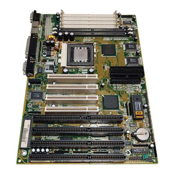
Page 9: P55-Tx 2 Layout
1-4 P55-TX 2 P55-TX 2 Layout SIMM 4 SIMM 3 SIMM 2 BANK2 SIMM 1 DIMM2 DIMM1 See Page MTXC See Page Secondary IDE Primary IDE See Page FDD CONN. PCI#4 See Page USB Conn. Winboand 83877F J 1 0... -
Page 10: Overview
Super I/O controller provides the standard PC I/O functions: a floppy interface, two 16-byte FIFO serial ports and an EPP/ECP capable parallel port. The P55-TX 2 layout is shown in the previous page for user's reference. Care must be taken when insert- ing memory modules, inserting CPU or even plugging PCI card into the associated slots to avoid damaging any circuits or sockets on board. - Page 11 P55-TX 2 The P55-TX 2 supports Award Plug & Play BIOS for the ISA and PCI cards. The BIOS can be located in Flash EPROM. The advantage of having Flash EPROM is much easier to replace BIOS code if necessary.
-
Page 12: Connectors And Jumpers
Hardware Design 2-2 Connectors and Jumpers This section describes all of the connectors and jumpers equipped in the mainboard. Please refer to Figure 1-1 for the location of each connector and jumper.The figure in the following means connecting pin 1&2 and means connecting pin 2&3. - Page 13 P55-TX 2 System Power ON/OFF Switch (For ATX Power Suppply Connector) Pressing the button once will switch the system on and enter the SLEEP MODE(Suspend mode). While in the SLEEP MODE, a keystrobe or mouse movement (mouse driver exists) will instantly "wake up"the system.
- Page 14 Hardware Design USB CONNECTOR: Reserved for USB port Adapter (refer to APPENDIX B:I/O Connectors) I/O back panel connector: PS/2 PS/2 COM2 COM1 parallel port Mouse Keyboard JP4:CPU Clock Rate Select. (Easy One Jumper Setting Only) Pentium Processor P54C / P55C Cyrix 6x86 / 6x86L / M2 AMD K5 / K6 IBM 6x86...
- Page 15 P55-TX 2 CPU Vcore voltage selection for Pentium MMX / AMD K6 / Cyrix 6X86L 1-6 : 2.0V for AMD K6 fast processor (Reserved) 2.0V 2-7 : 2.8V for Pentium P55C(MMX)/Cyrix 6X86L(Dual Voltage) 2.8V 2.9V 3-8 : 2.9V for AMD K6 PR166/PR200 or 6X86MX-PR166/PR200/ 3.2V...
-
Page 16: Real Time Clock Battey Replacement
Hardware Design Real Time Clock Battery Replacement The battery can be replaced by a Sanyo / Panasonic CR2032, or other equivalent coin lithium battery. Please follow the steps below to replace the battery. 2.Insert 1.Remove... -
Page 17: System Memory Configuration
P55-TX 2 2-4 System Memory Configuration The P55-TX 2 supports different types of settings for the system memory. Jumper JP7 for SDRAM hardware setting is for memory configuration. The following figures show all possible memory combinations. SIMM4 > BANK 1... -
Page 18: Cache Memory Configuration
DIMM module is 3.3V/Unbuffered to supports Intel Pentium Processor System or 5V Fast Page, EDO DRAM. * P55-TX 2 Supports and extends many memory configurations on its 2 SIMM and 2 DIMM sites. The memory size of any configuration can be combined flexibly. -
Page 19: Integrated Pci Bridge
Revision 2.1 Compliant and contains a Universal Serial Bus interface with both host and hub control functions. P55-TX 2 reserves a USB connector to provide two USB ports for serial transfer at 12 or 1.5 Mbit/sec. This supports legacy keyboard and mouse software with USB-Base Keyboard and mouse. - Page 20 ATX Form-Factor Overvirw The P55-TX 2 is base on ATX form-factor with a board size 8.2" x 12" (208mm x 305mm). The ATX from-factor is essentially an enlarged baby-AT basedboard rotated 90 degrees within an ATX chassis and uses ATX power supply. The changes make pentium processor able to locate away from the expansion slots and all onboard I/Os able to hold full length add-on cards.
- Page 21 3-2 P55-TX 2 The P55-TX 2 is equipped with a standard I/O back pannel featuring a serial port, PS/2 mouse port, PS/2 keyboard port, parallel port, and secondary serial port (refer to Figure 3-2 ). PS/2 PS/2 COM2 COM1 parallel port...
-
Page 22: External Madem Ring-In Power-On And Keyboard Power-On Functions
On the basis of bounded functions in I/O chipset, the two serial ports are able to support the External Modem Ring-in Power ON function. Once users connect the external modem to COM1 or COM2, the P55-TX 2 mainboard allows them to turn on their system through the remote and host's dial-up control. -
Page 23: Chapter 4 - Award Bios Setup
AWARD BIOS 4-1 Chapter 4 Award BIOS Setup Award's ROM BIOS provides a built-in Setup program which allows user to modify the basic system configuration and hardware parameters. The modified data will be stored in a battery-backed CMOS RAM so data will be retained even when the power is turned off. -
Page 24: Standard Cmos Setup
This menu shows all of the manufacturer's default values of P55-TX 2. Again, user can move the cursor by pressing direction keys and <PgDn> or <PgUp> keys to modify the parameters. Pressing [F1] key to display help message of the selected item. - Page 25 AWARD BIOS 4-3 ROM PCI/ISA BIOS(2A59IPA9) BIOS FEATURES SETUP AWARD SOFTWARE, INC. Virus Warning : Disabled Video BIOS Shadow : Enabled CPU Internal Cache : Enabled C8000-CBFFF Shadow : Disabled External Cache : Enabled CC000-CFFFF Shadow : Disabled Quick Power On Self Test : Enabled D0000-D3FFF Shadow...
- Page 26 4-4 CHAPTER 4 Quick Power On Self Test:This category speeds up Power On Self Test (POST) after you power on the computer. If it is set to Enabled, BIOS will shorten or skip some check items during POST. The default is Enabled. Enabled : Enable quick POST.
- Page 27 AWARD BIOS 4-5 Gate A20 Option This refers to the way the system addresses memory above 1MB (extended memory). The default value is Fast. Normal The A20 signal is controlled by keyboard controller or chipset hardware. Fast : The A20 signal is controlled by Port 92 or chipset specific method. Typematic Rate Setting This determines the keystroke repeat rate.
-
Page 28: Chipset Features Setup
4-6 CHAPTER 4 C8000 - CBFFF Shadow : CC000 - CFFFF Shadow: D0000 - D3FFF Shadow: D4000 - D7FFF Shadow: D8000 - DBFFF Shadow: DC000 - DFFFF Shadow: These categories determine whether other expansion card optional ROM will be copied to RAM by 16K byte or 32K byte per unit and the size depends on chipset. If you install other expansion cards with ROMs on them, you will need to know which addresses the ROMs use to shadow themselves specifically. - Page 29 AWARD BIOS 4-7 Note: When you insert slow memory modules in the system and set a faster timing, the system may hang up. DRAM Timing: The default value is 60ns. 60ns : 2 (faster) Burst Wait State, for 60~70ns Fast Page Mode/EDO DRAM. 70ns : 3 (slower) Burst Wait State, for 70ns Fast Page Mode/EDO DRAM.
-
Page 30: Power Management Setup
4-8 CHAPTER 4 : The default value is enabled. Video BIOS Cacheable Enabled : This field Enables the Video BIOS Cacheable to speed up the VGA Performance. Disabled: Disables the Video BIOS Cacheable function. 8/16 Bit I/O Recovery Time: The default value is 1. 8 Bit I/O Recovery Time: This field defines the recovery time from 1 to 8 for 8- bit I/O. - Page 31 AWARD BIOS 4-9 ROM PCI/ISA BIOS (2A59IPA9) POWER MANAGEMENT SETUP AWARD SOFTWARE, INC. Power Management : User Define ** Reload Global Timer Events ** PM Control by APM : Yes IRQ [3-7, 9-15], NMI : Enabled Video off Method : V/H SYNC+Blank Primary IDE 0 : Disabled Video off After : Standby...
- Page 32 4-10 CHAPTER 4 B. Time-out parameters : HDD Standby The HDD Standby timer can be set from 1 to 15 minute(s). System Doze The "System Doze" mode timer starts to count when no "PM event" occurres. The valid time-out setting is from 1 minute up to 1 hour. System Standby The "Standby"...
-
Page 33: Plug & Play/Pci Configuration
AWARD BIOS 4-11 The P55-TX 2 supports HDD Power Down, Doze and standby power saving functions when Intel Pentium Processor is installed. In addition, the suspend function is supported when the JP14's sleep (sleep ref. Figure1-1) is closed to enter the green function. - Page 34 4-12 CHAPTER 4 ROM PCI/ISA BIOS(2A59CPA9) PNP/PCI CONFIGURATION AWARD SOFTWARE, INC. PNP OS Installed : NO PCI IDE IRQ Map To : PCI-AUTO Resources Controlled By : Manual Primary IDE INT# Reset Configuration Data : Disabled Secondary IDE INT# IRQ-3 assigned to : Legacy ISA IRQ-4...
- Page 35 AWARD BIOS 4-13 Used MEM base addr and Used MEM Length : The default value is N/A. The Used MEM base addr (CB00, CC00, D000, D400, D800, DC00) and Used MEM Length (8K, 16K, 32K, 64K) support some specific ISA Legacy cards with requested memory space below 1M address.
-
Page 36: Integrated Peripherals
4-14 CHAPTER 4 Integrated Peripherals ROM PCI/ISA BIOS(2A59IPA9) INTEGRATED PERIPHERALS WARD SOFTWARE, INC. IDE HDD Block Mode : Enabled Onboard Parallel Mode : ECP / EPP IDE Primary Master PIO : Auto ECP Mode Ise DMA IDE Primary Slave PIO : Auto Parallel Port EPP Type : EPP1.9... - Page 37 AWARD BIOS 4-15 IDE Primary Master PIO: The default value is Auto. Auto : BIOS will automatically detect the Onboard Primary Master PCI IDE HDD Accessing mode. Mode0~4 : Manually set the IDE Accessing mode. IDE Primary Slave PIO: The default value is Auto. Auto : BIOS will automatically detect the Onboard Primary Slave PCI IDE HDD Accessing mode.
-
Page 38: Load Setup Defaults
4-16 CHAPTER 4 Onboard UART 2 Mode:The default value is standard. This field allows the user to select the COM2 port that can support a serial Infrared Interface. Standard:Support a Serial Infrared Interface IrDA. HPSIR:Support a HP Serial Infrared Interface formats. ASKIR:Support a Sharp Serial Infrared Interface formats. -
Page 39: Change Supervisor Or User Password
AWARD BIOS 4-17 ROM PCI/ISA BIOS(2A59IPA9) CMOS SETUP UTILITY AWARD SOFTWARE, INC. STANDARD CMOS SETUP SUPERVISOR PASSWORD BIOS FEATURES SETUP USER PASSWORD CHIPSET FEATURES SETUP IDE HDD AUTO DETECTION POWER MANAGEMENT SETUP HDD LOW LEVEL FORMAT PNP/PCI CONFIGURA ETUP Load SETUP Default (Y/N)? INTEGRATED PERIPH SAVING LOAD SETUP DEFAULTS... -
Page 40: Ide Hdd Auto Detection
4-18 CHAPTER 4 4-9 IDE HDD Auto Detection The "IDE HDD AUTO DETECTION" utility is a very useful tool especially when you do not know which kind of hard disk type you are using. You can use this utility to detect the correct disk type installed in the system automatically. - Page 41 AWARD BIOS 4-19 LBA (Logical Block Addressing) mode: A new HDD accessing method to overcome the 528 Megabyte bottleneck. The numbers of cylinders, heads and sectors shown in the setup may not be the numbers physically contained in the HDD. During HDD accessing, the IDE controller will transform the logical address described by sector, head and cylinder into its own physical address inside the HDD.
-
Page 42: Hdd Low Level Format
4-20 CHAPTER 4 Note: To support LBA or LARGE mode of HDDs, there must be some softwares involved. All these softwares are located in the Award HDD Service Routine (1NT 13h). It may be failed to access a HDD with LBA (LARGE) mode selected if you are running under an Operating System which replaces the whole 1NT 13h. -
Page 43: Chapter 5 - Technical Information
TECHNICAL INFORMATION 5-1 Chapter 5 Technical Information 5-1 I/O & MEMORY MAP MEMORY MAP Address Range Size Description [00000-7FFFF] 512K Conventional memory [80000-9FBFF] 127K Extended Conventional memory [9FC00-9FFFF] Extended BIOS data area if PS/2 mouse is installed [A0000-C7FFF] 160K Available for Hi DOS memory [C8000-DFFFF] Available for Hi DOS memory and adapter ROMs [E0000-EEFFF]... -
Page 44: Time & Dma Channels Map
5-2 CHAPTER 5 5-2 Time & DMA Channels Map TIME MAP: TIMER Channel 0 System timer interrupt. TIMER Channel 1 DRAM REFRESH request. TIMER Channel 2 SPEAKER tone generator. DMA CHANNELS : DMA Channel 0 Available. DMA Channel 1 Onboard ECP (Option). DMA Channel 2 FLOPPY DISK (SMC CHIP). -
Page 45: Rtc & Cmos Ram Map
TECHNICAL INFORMATION 5-3 5-4 RTC & CMOS RAM Map RTC & CMOS : Seconds. Second alarm. Minutes. Minutes alarm. Hours. Hours alarm. Day of week. Day of month. Month. Year. Status register A. Status register B. Status register C. Status register D. Diagnostic status byte. -
Page 46: Appendix A: Post Codes
5-4 CHAPTER 5 Appendix A: POST Codes ISA POST codes are typically output to port address 80h. POST(hex) DESCRIPTION 01-02 Reserved. Turn off OEM specific cache, shadow. 1.Initialize EISA registers (EISA BIOS only). 2.Initialize all the standard devices with default values Standard devices includes. -DMA controller (8237). - Page 47 TECHNICAL INFORMATION 5-5 POST(hex) DESCRIPTION Initialization of the BIOS Data Area. (40:ON - 40:FF) 1.Program some of the Chipset's value according to Setup (Early Setup Value Program). 2.Measure CPU speed for display and decide the system clock speed. 3.Video initialization including Monochromc, CGA and EGA/VGA. If no display device found, the speaker will beep up.
- Page 48 5-6 CHAPTER 5 POST(hex) DESCRIPTION 1.Display the Award Plug & Play BIOS Extension message (PnP BIOS only). 2.Program all onboard super I/O chips (if any) including COM ports, LPT ports, FDD port ... according to setup value. 33-3B Reserved. Set flag to allow users to enter CMOS Setup Utility. 1.Initialize Keyboard.
- Page 49 TECHNICAL INFORMATION 5-7 POST(hex) DESCRIPTION 1.Initialize all ISA ROMs. 2.Later PCI initializations (PCI BIOS only). -Assign IRQ to PCI devices. -Initialize all PCI ROMs. 3.PnP Initialzations. (PnP BIOS only) -Assign IO, Memory, IRQ & DMA to PnP ISA devices. -Initialize all PnP ISA ROMs. 4.Program shadows RAM according to Setup settings.
-
Page 50: Appendix B: I/O Connectors
5-8 CHAPTER 5 Appendix B: I/O Connectors JP13 : PS/2 Mouse Connector: Signal Name Data (Red Wire) Clock (Blue Wire) (Green Wire) (Yellow Wire) JP10/COM1, JP11/COM2 : Serial Ports Connector Signal Name Signal Name SOUT J8 : Parallel Port Connector Signal Name Signal Name STROBE-... - Page 51 TECHNICAL INFORMATION 5-9 J7 : Floppy Disk Connector Signal Name Signal Name Ground FDHDIN Ground Reserved Ground FDEDIN Ground Index- Ground Motor Enable Ground Drive Select B- Ground Drive Select A- Ground Motor Enable Ground DIR- Ground STEP- Ground Write Data Ground Write Gate Ground...
- Page 52 5-10 CHAPTER 5 ATX Power Supply Connector: Signal Name Signal Name 3.3V 3.3V -12.0V 3.3V PS-ON 5.0V 5.0V -5.0V PW-OK 5.0V 5VSB 5.0V 12.0V CN1: USB Connector: USB Port 1 USB Port 2 PS/2 Mouse Figure 5-1 USB Port Adapter...
Need help?
Do you have a question about the P55-TX 2 and is the answer not in the manual?
Questions and answers