Table of Contents
Advertisement
SERVICE MANUAL
• This set is the Amplifier and CD player
section in CMT-RB5.
Main Unit
Amplifier section
For the U.S. model
AUDIO POWER SPECIFICATIONS
POWER OUTPUT AND TOTAL HARMONIC
DISTORTION:
With 4-ohm loads, both channels driven, from
120 – 10,000 Hz; rated 15 watts per channel
minimum RMS power, with no more than 10%
total harmonic distortion from 250 milliwatts to
rated output.
US, Canadian and Mexican models:
Continuous RMS power output (reference):
15 + 15 watts
(4 ohms at 1 kHz, 10% THD)
European and Australian models:
DIN power output (Rated):12 + 12 watts
(4 ohms at 1 kHz, DIN)
Continuous RMS power output (Reference):
15 + 15 watts
(4 ohms at 1 kHz,
10% THD)
Music power output (Reference):
28 + 28 watts
Other models:
The following measured at 220 V AC, 50/60 Hz
DIN power output (rated): 10 + 10 watts
(4 ohms at 1 kHz, DIN)
Continuous RMS power output (reference):
12 + 12 watts
(4 ohms at 1 kHz, 10% THD)
The following measured at 240 V AC, 50/60 Hz
DIN power output (rated): 12 + 12 watts
(4 ohms at 1 kHz, DIN)
Continuous RMS power output (reference):
15 + 15 watts
(4 ohms at 1 kHz, 10% THD)
HCD-RB5
Model Name Using Similar Mechanism NEW
CD Mechanism Type
Base Unit Name
Optical Pick-up Name
SPECIFICATIONS
Inputs
MD/VIDEO (AUDIO) IN (phono jacks):
voltage 500/250 mV, impedance
47 kilohms
Outputs
MD/VIDEO (AUDIO) OUT (phono jack):
voltage 250 mV, impedance
1 kilohm
PHONES (stereo minijack):
accepts headphones of 8 ohms or
more.
SPEAKER:
accepts impedance of 4 to
16 ohms.
CD DIGITAL OUT OPTICAL:
Optical
CD player section
System
Compact disc and digital audio
system
Laser
Semiconductor laser (λ=780 nm)
Emission duration: continuous
MAX. 44.6 µW*
Laser output
*This output is the value measured
at a distance of 200 mm from the
objective lens surface on the
Optical Pick-up Block with 7 mm
aperture.
Frequency response
2 Hz – 20 kHz
Tuner section
FM stereo, FM/AM superheterodyne tuner
FM tuner section
Tuning range
US, Canadian model:
87.5 – 108.0 MHz
(100 kHz step)
Other models:
87.5 – 108.0 MHz
(50 kHz step)
Antenna
FM lead antenna
Antenna terminals
75 ohms unbalanced
Intermediate frequency
10.7 MHz
MICRO Hi-Fi COMPONENT SYSTEM
US Model
Canadian Model
AEP Model
UK Model
E Model
Australian Model
Chinese Model
CDM55C-K6BD38
BU-K6BD38
KSM-213DCP
AM tuner section
Tuning range
US, Canadian model:
530 – 1,710 kHz
(with the interval set at 10 kHz)
531 – 1,710 kHz
(with the interval set at 9 kHz)
European model:
531 – 1,602 kHz
(with the interval set at 9 kHz)
Other models:
531 – 1,602 kHz
(with the interval set at 9 kHz)
530 – 1,710 kHz
(with the interval set at 10 kHz)
Antenna
AM loop antenna
External antenna terminals
Intermediate frequency
450 kHz
General
Power requirements
US, Canadian model:
120 V AC, 60 Hz
European model:
230 V AC, 50/60 Hz
Australian model:
220 – 240 V AC, 50/60 Hz
Korea, Chinese model:
220 V AC, 50/60 Hz
Mexican model:
120 V AC, 60 Hz
Other models:
110 – 120 V or 220 – 240 V AC,
50/60 Hz
Adjustable with voltage selector
Power consumption
US, Canadian and Mexican models:
50 watts
Other models:
45 watts
Approx. 180 × 130 × 315 mm
Dimensions (w/h/d)
incl. projecting parts and controls
Mass
Approx. 4.0 kg
Supplied accessories
Remote (1)
Size AA (R6) batteries (2)
AM loop antenna (1)
FM lead antenna (1)
Speaker cords (2)
Design and specifications are subject to change
without notice.
Advertisement
Table of Contents

Related Manuals for Sony HCD-RB5


Summary of Contents for Sony HCD-RB5
-
Page 1: Specifications
HCD-RB5 SERVICE MANUAL US Model Canadian Model AEP Model UK Model E Model Australian Model Chinese Model • This set is the Amplifier and CD player section in CMT-RB5. Model Name Using Similar Mechanism NEW CD Mechanism Type CDM55C-K6BD38 Base Unit Name... -
Page 2: Table Of Contents
TABLE OF CONTENTS 1. GENERAL ·········································································· 4 NOTES ON HANDLING THE OPTICAL PICK-UP BLOCK OR BASE UNIT 2. DISASSEMBLY ································································ 6 The laser diode in the optical pick-up block may suffer electrostatic break-down because of the potential difference generated by the 3. -
Page 3: Leakage Test
LES COMPOSANTS IDENTIFÉS PAR UNE MARQUE 0 SUR LES DIAGRAMMES SCHÉMATIQUES ET LA LISTE DES PIÈCES SONT CRITIQUES POUR LA SÉCURITÉ DE FONCTIONNEMENT. NE REMPLACER CES COMPOSANTS QUE PAR DES PIÈSES SONY DONT LES NUMÉROS SONT DONNÉS DANS CE MANUEL OU DANS LES SUPPÉMENTS PUBLIÉS PAR SONY. -
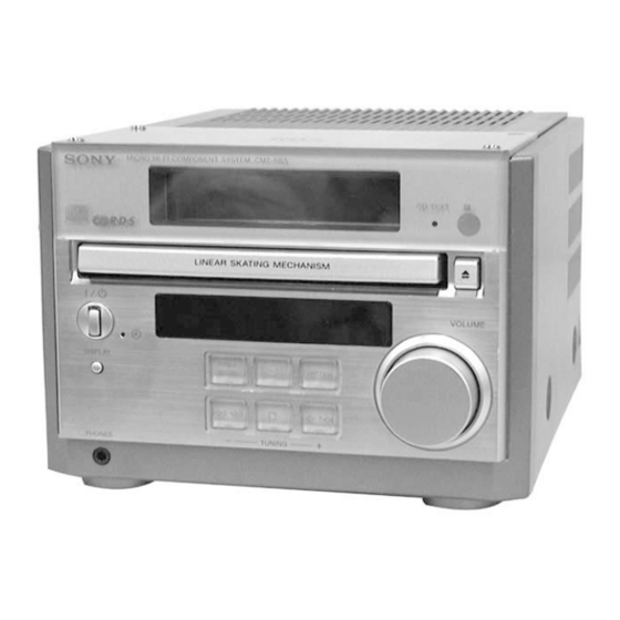
Page 4: General
SECTION 1 GENERAL LOCATION OF CONTROLS – Front Panel – 1 ?/1 button 2 DISPLAY button 3 TUNER/BAND button 4 7 button 5 FUNCTION button 6 Z button 7 VOLUME knob 8 J L button 9 s button q; l j button qa PHONE jack qs t indicator... - Page 5 This section is extracted from instruction manual. If you made a mistake Step 2: Setting the time Press m/M repeatedly until the incorrect item flashes, then set it again. You must set the time beforehand to use the timer To change the preset time functions.
-
Page 6: Disassembly
SECTION 2 DISASSEMBLY Note: Follow the disassembly procedure in the numerical order given. 2-1. CASE (TOP) 7 one screw (BVTP3 × 10) 8 case (left) qa case (top) q; one screw 6 two case screws (BVTP3 × 10) qs back panel 9 eight screws (BVTP3 ×... - Page 7 2-3. CD MECHANISM DECK (CDM55C-K6BD38) 3 screw (BVTP3 × 8) 4 CD mechanism deck (CDM55C-K6BD38) 1 wire (flat type) (19 core)(CN401) 2 connector (CN1) 2-4. BASE UNIT (BU-K6BD38) 1 floating screw (PTPWHM2.6) 2 base unit (BU-K6BD38)
- Page 8 2-5. LOADING BOARD 2 belt (CDM55) 1 Rotate the gear(B) in the direction of arrow A . 3 Pull the tray pushing B . 5 LOADING board 4 two screws (BTP2.6 × 6) 2-6. CAM (CDM55C-K6BD38) 3 spacer (55) 4 pulley (LDG) 6 gear (B) 5 gear (A) 1 torsion spring...
-
Page 9: Service Mode
SECTION 3 SERVICE MODE [Panel Test Mode] [Aging Mode] This mode can be used for operation check of CD section. Procedure: 1. Set to standby state. Procedure: 2. Press three buttons of s , ?/1 , and 7 simultaneously. 1. Load a CD disc. 3. -
Page 10: Electrical Adjustments
SECTION 4 ELECTRICAL ADJUSTMENTS Note : Clear RF signal waveform means that the shape “ ◊ ” can be clearly CD SECTION distinguished at the center of the waveform. Note : RF signal waveform 1. CD Block is basically designed to operate without adjustment. VOLT/DIV : 200mV Therefore, check each item in order given. -
Page 11: Diagrams
HCD-RB5 SECTION 5 DIAGRAMS NOTE FOR PRINTED WIRING BOARDS AND SCHEMATIC DIAGRAMS 5-1. Wavefoarms Note on Printed Wiring Board: Note on Schematic Diagram: – BD BOARD – – MAIN BOARD – • X : parts extracted from the component side. -
Page 12: Printed Wiring Board -Bd Section
HCD-RB5 • See page 11 for Circuit Boards Location. 5-3. PRINTED WIRING BOARD –BD SECTION– • Semiconductor Location Ref. No. Location IC101 IC102 IC103 TP(TE0) (VC) Q101 TP(FE0) (RF) TP(FE1) TP(AGC CON) TP(D GND) (XPCK) (Page 14) -
Page 13: Schematic Diagram -Bd Section
HCD-RB5 5-4. SCHEMATIC DIAGRAM –BD SECTION– • See page 11 for Waveforms. • See page 22 for IC Block Diagrams. -
Page 14: Main Section
HCD-RB5 • See page 11 for Circuit Boards Location. 5-5. PRINTED WIRING BOARDS –MAIN SECTION– There are a few cases that the part printed on this diagram isn’t mounted in this model. • Semiconductor Location Ref. No. Location Ref. No. Location... -
Page 15: Main Section(1/2)
HCD-RB5 5-6. SCHEMATIC DIAGRAM –MAIN SECTION(1/2)– • See page 11 for Waveforms. • See page 20 for IC Pin Function. PIN FUNCTION... -
Page 16: Main Section(2/2)
HCD-RB5 • See page 22 for IC Block Diagrams. 5-7. SCHEMATIC DIAGRAM –MAIN SECTION(2/2)–... -
Page 17: Power Section
HCD-RB5 5-8. PRINTED WIRING BOARDS –POWER SECTION– • See page 11 for Circuit Boards Location. There are a few cases that the part printed on this diagram isn’t mounted in this model. VOLTAGE SELECTOR 110-120V 220-240V (Page 14) (Page 14) -
Page 18: Panel Section
HCD-RB5 • See page 11 for Circuit Boards Location. 5-9. PRINTED WIRING BOARD –PANEL SECTION– There are a few cases that the part printed on this diagram isn’t mounted in this model. • Semiconductor Location Ref. No. Location D801 D805... -
Page 19: Panel Section
HCD-RB5 5-10. SCHEMATIC DIAGRAM –PANEL SECTION–... -
Page 20: Loading Section
HCD-RB5 • See page 11 for Waveforms. 5-11. SCHEMATIC DIAGRAM –LOADING SECTION– 5-13. IC Pin Function • MAIN BOARD IC601 M30622MAA-A64FP (SYSTEM CONTROLLER) Pin No. Pin Name Description STKPOWER Not used. OPEN B-SHUT Not used. OPEN SPEAKER RELAY FRONT-RELAY ON(H)/OFF(L) H.PHONE DETECT... - Page 21 Pin No. Pin Name Description TUNED TUNED IN(L)/OFF(H) ST-CE TUNER CHIP ENB ST-DOUT TUNER DATA OUT ST-DIN TUNER DATA IN ST-CLK TUNER CLOCK SENS From CXP2587 SENS HOLD MODE XLTAT CD LAT XRST CD RESET Not used. OPEN Not used. OPEN —...
-
Page 22: Ic Block Diagrams
5-14. IC BLOCK DIAGRAMS — BD BOARD — IC101 CXD2587Q ERROR DIGITAL CORRECTOR ASYMMETRY DIGITAL CORRECTION OPERATIONAL LRCK AMPLIFIER ANALOG SWITCH PCMD INTERFACE DEMODULATOR CONVERTER EMPH XVDD XTAI TIMING CLOCK XTAO LOGIC XTSL GENERATOR XVSS TES1 AVDD1 TEST AOUT1 SERVO DSP PWM GENERATOR AIN1 FRDR... -
Page 23: Exploded Views
SECTION 6 EXPLODED VIEWS NOTE: • -XX, -X mean standardized parts, so they may • Abbreviation The components identified by mark 0 or have some differences from the original one. CND : Canadian model. dotted line with mark 0 are critical for safety. •... -
Page 24: Front Panel Section
6-2. FRONT PANEL SECTION Supplied with MAIN board. z A : PANEL board z B : LED board z C : H.P. board supplied Ref. No. Part No. Description Remarks Ref. No. Part No. Description Remarks 4-230-213-01 WINDOW (TOP) 4-951-620-01 SCREW (2.6X8), +BVTP (US,CND,E,MX,AR,HK,SP,MY,KR,TW,AUS,CH) 4-933-134-11 SCREW (+PTPWH M2.6X8) 4-230-213-11 WINDOW (TOP) (AEP,UK,AED,EE,CIS) -
Page 25: Chassis Section
6-3. CHASSIS SECTION not supplied Supplied with MAIN board. z D : BACK PANEL board not supplied not supplied CDM55C-K6BD38 not supplied not supplied not supplied T901 not supplied not supplied not supplied Ref. No. Part No. Description Remarks Ref. No. Part No. - Page 26 6-4. CD MECHANISM DECK SECTION (CDM55C-K6BD38) not supplied M901 BU-K6BD38 Ref. No. Part No. Description Remarks Ref. No. Part No. Description Remarks 4-224-894-11 TRAY (CDM55D) 1-674-336-21 LOADING BOARD 4-220-229-01 LEVER (SW) 4-221-815-01 ROLLER 4-220-239-11 SPRING, TORSION 7-685-534-19 SCREW +BTP 2.6X8 TYPE2 N-S 4-221-816-11 BELT (CDM55) X-4953-195-1 PULLEY (AT) ASSY 4-220-234-01 PULLEY (LDG)
- Page 27 6-5. BASE UNIT SECTION (BU-K6BD38) Ref. No. Part No. Description Remarks Ref. No. Part No. Description Remarks 4-985-672-01 SCREW (+PTPWHM2.6), FLOATING 1-792-024-11 WIRE (FLAT TYPE) (16 CORE) 4-227-679-01 INSULATOR (213) 4-229-806-01 SPRING (213), COMPRESSION 0 203 8-820-116-01 OPTICAL PICK-UP KSM-213DCP/Z-NP X-4953-169-1 HOLDER (BU) ASSY A-4724-934-A BD BOARD, COMPLETE 4-951-620-01 SCREW (2.6X8), +BVTP...
-
Page 28: Electrical Parts List
SECTION 7 BACK PANEL ELECTRICAL PARTS LIST NOTE: • Due to standardization, replacements in the • Abbreviation • SEMICONDUCTORS parts list may be different from the parts CND : Canadian model. In each case, u: µ, for example: specified in the diagrams or the components : Australian model. - Page 29 H.P. LODAING Ref. No. Part No. Description Remarks Ref. No. Part No. Description Remarks C133 1-164-346-11 CERAMIC CHIP R158 1-216-111-00 METAL CHIP 390K 1/10W C140 1-164-346-11 CERAMIC CHIP R159 1-216-101-00 METAL CHIP 150K 1/10W C141 1-164-346-11 CERAMIC CHIP R162 1-216-101-00 METAL CHIP 150K 1/10W C143...
- Page 30 MAIN Ref. No. Part No. Description Remarks Ref. No. Part No. Description Remarks A-4475-310-A MAIN BOARD, COMPLETE (US,CND) C251 1-126-964-11 ELECT 10uF 20.00% 50V C252 1-136-172-00 MYLAR 0.39uF 5.00% 50V ********************* A-4475-315-A MAIN BOARD, COMPLETE (AEP,UK,AED,EE,CIS) C253 1-136-165-00 MYLAR 0.1uF 5.00% 50V C254 1-130-476-00 MYLAR...
- Page 31 MAIN Ref. No. Part No. Description Remarks Ref. No. Part No. Description Remarks C611 1-126-934-11 ELECT 220uF 20.00% 10V IC202 8-759-634-51 IC M5218AP C612 1-126-916-11 ELECT 1000uF 20.00% 6.3V IC301 8-759-333-24 IC LM1876TF C613 1-164-159-11 CERAMIC 0.1uF IC501 8-759-822-09 IC LB1641 IC551 8-759-635-63 IC M51943BSL-TP <...
- Page 32 MAIN Ref. No. Part No. Description Remarks Ref. No. Part No. Description Remarks R215 1-249-430-11 CARBON 1/4W R472 1-249-437-11 CARBON 1/4W R216 1-249-417-11 CARBON 1/4W F R501 1-247-807-31 CARBON 1/4W R217 1-249-417-11 CARBON 1/4W F R551 1-247-807-31 CARBON 1/4W R218 1-249-425-11 CARBON 4.7K 1/4W F...
- Page 33 MAIN PANEL Ref. No. Part No. Description Remarks Ref. No. Part No. Description Remarks R646 1-247-807-31 CARBON 1/4W PANEL BOARD R647 1-249-417-11 CARBON 1/4W F *********** R648 1-247-807-31 CARBON 1/4W (Supplied with MAIN board) R649 1-249-417-11 CARBON 1/4W F R650 1-247-807-31 CARBON 1/4W 4-212-590-22 HOLDER (FL)
- Page 34 HCD-RB5 PANEL Ref. No. Part No. Description Remarks Ref. No. Part No. Description Remarks R817 1-249-415-11 CARBON 1/4W F 1-757-267-11 WIRE, FLAT TYPE (19 CORE) R821 1-247-807-31 CARBON 1/4W 1-757-266-11 WIRE, FLAT TYPE (13 CORE) R822 1-247-807-31 CARBON 1/4W 1-769-980-11 WIRE (FLAT TYPE) (13 CORE)