Table of Contents
Advertisement
Service
Manual
HEAD UNIT(3 in 1)
FX-M2017
VEHICLE
DESTINATION
SAAB 9-5
EUROPE
- This service manual should be used together with the following manual(s):
Model No.
Order No.
CX-1011
CRT2406
CX-958
CRT2423
- Dolby noise reduction manufactured under license from Dolby Laboratories Licensing Corporation.
"Dolby" and the double-D symbol are trademarks of Dolby Laboratories Licensing Corporation.
CONTENTS
1. SAFETY INFORMATION ............................................2
2. EXPLODED VIEWS AND PARTS LIST .......................3
4. PCB CONNECTION DIAGRAM ................................30
5. ELECTRICAL PARTS LIST ........................................48
6. ADJUSTMENT..........................................................58
7. GENERAL INFORMATION .......................................64
7.1 DIAGNOSIS ........................................................64
7.1.1 TEST MODE ..............................................64
PIONEER CORPORATION
PIONEER ELECTRONICS (USA) INC.
Haven 1087 Keetberglaan 1, 9120 Melsele, Belgium
PIONEER EUROPE NV
PIONEER ELECTRONICS ASIACENTRE PTE.LTD. 253 Alexandra Road, #04-01, Singapore 159936
C PIONEER CORPORATION 2001
SAAB
PRODUCED AFTER
2001
Mech. Module Remarks
3L
Cassette Mech. Module:Mech.Description, Disassembly
S8.1
CD Mech. Module:Circuit Description, Mech.Description, Disassembly
4-1, Meguro 1-Chome, Meguro-ku, Tokyo 153-8654, Japan
P.O.Box 1760, Long Beach, CA 90801-1760 U.S.A.
ZSA
SAAB PART No.
ID No.
5038120
7.1.2 DISASSEMBLY .........................................65
7.1.3 PCB LOCATIONS ......................................70
7.2 IC .......................................................................72
7.3 EXPLANATION ...................................................78
7.3.1 OPERATIONAL FLOW CHART .................78
7.3.2 SYSTEM BLOCK DIAGRAM.....................79
7.3.3 JIG CONNECTION DIAGRAM..................79
8. OPERATIONS AND SPECIFICATIONS.....................80
ORDER NO.
CRT2741
X1B/EW
PIONEER MODEL No.
FX-M2017ZSA/X1B/EW
K-ZZY. AUG. 2001 Printed in Japan
Advertisement
Table of Contents

Subscribe to Our Youtube Channel
Related Manuals for Pioneer FX-M2017ZSA X1B


Summary of Contents for Pioneer FX-M2017ZSA X1B
-
Page 1: Table Of Contents
PIONEER ELECTRONICS (USA) INC. P.O.Box 1760, Long Beach, CA 90801-1760 U.S.A. Haven 1087 Keetberglaan 1, 9120 Melsele, Belgium PIONEER EUROPE NV PIONEER ELECTRONICS ASIACENTRE PTE.LTD. 253 Alexandra Road, #04-01, Singapore 159936 C PIONEER CORPORATION 2001 K-ZZY. AUG. 2001 Printed in Japan... -
Page 2: Safety Information
FX-M2017ZSA - CD Player Service Precautions 2. During disassembly, be sure to turn the power off 1. For pickup unit(CXX1285) handling, please refer since an internal IC might be destroyed when a con- to"Disassembly"(see page 65). nector is plugged or unplugged. During replacement, handling precautions shall be 3. -
Page 3: Exploded Views And Parts List
FX-M2017ZSA 2. EXPLODED VIEWS AND PARTS LIST 2.1 PACKING NOTE: - Parts marked by “*” are generally unavailable because they are not in our Master Spare Parts List. ∇ mark on the product are used for disassembly. - Screws adjacent to PACKING SECTION PARTS LIST Mark No. - Page 4 FX-M2017ZSA 2.2 EXTERIOR...
- Page 5 FX-M2017ZSA - EXTERIOR SECTION PARTS LIST Mark No. Description Part No. Mark No. Description Part No. 1 Screw BSZ26P050FMC 48 Insulator CNM5452 2 Screw BMZ30P050FMC 49 Insulator CNM5453 3 Connector UDE-039 50 Insulator CNM5135 51 Insulator CNM5136 4 Connector CDE4952 5 Case CNB1958 52 Insulator...
- Page 6 FX-M2017ZSA 2.3 CD MECHANISM MODULE...
- Page 7 FX-M2017ZSA - CD MECHANISM MODULE SECTION PARTS LIST Mark No. Description Part No. Mark No. Description Part No. 1 Control Unit CWX2411 46 ••••• 2 Connector(CN802) CKS2192 47 Ball CNR1189 48 Belt CNT1086 3 Connector(CN801) CKS2193 4 Connector(CN701) CKS2773 49 Roller CNV4509 5 Connector(CN101) CKS3486...
- Page 8 FX-M2017ZSA 2.4 CASSETTE MECHANISM MODULE...
- Page 9 FX-M2017ZSA - CASSETTE MECHANISM MODULE SECTION PARTS LIST Mark No. Description Part No. Mark No. Description Part No. 1 Screw BSZ20P040FMC 46 Pinch Roller ENV1518 2 Washer CBF1037 47 Pinch Holder Unit EXA1607 3 Washer CBG1003 48 Pinch Roller ENV1518 4 Screw EBA1028 49 Reel Unit...
-
Page 10: Block Diagram And Schematic Diagram
FX-M2017ZSA 3. BLOCK DIAGRAM AND SCHEMATIC DIAGRAM 3.1 BLOCK DIAGRAM TUNER MOTHER PCB TUNER UNIT FM IF FILTER FM IF FM IF OUT CN501 CF51 FM IF FM RF Q471 Q553 Q554 FM IF FM MIX CF52 CF53 FM ANT T551 AM ANT Q473... -
Page 11: Keyboard Unit
FX-M2017ZSA CONNECTOR PCB TEL AUDIO ISOLATOR CN801 CN852 TELG TELG IC 471 TELAU NJM4558MD TELAU CDML+ CDM+ CDML- CDM- ELECTRONIC VOLUME CONTROL FRONT AUDIO OUTPUT CDM- IC 401 CON C CDM+ 25 26 NJM4558MD IC 405 TU/TEL SN761029DL CANH 22 23 24 25 26 REAR AUDIO OUTPUT CANL 17 18 19 20 21... - Page 12 FX-M2017ZSA 3.2 OVERALL CONNECTION DIAGRAM(GUIDE PAGE) Note: When ordering service parts, be sure to refer to “EXPLODED VIEWS AND PARTS LIST” or “ELECTRICAL PARTS LIST”. TUNER MOTHER PCB Large size SCH diagram : FM, AM SIGNAL TUNER UNIT : TAPE SIGNAL : CD SIGNAL CN501 : AUDIO SIGNAL...
- Page 13 FX-M2017ZSA ELECTRONIC VOLUME AUDIO OUTPUT (UNBAL/BAL) R469 FM : -28dBs 6R8K AM : -28dBs FM : -6dBs CD : 3.8dBs AM : -6dBs TAPE : -7.9dBs CD : 7.8dBs TAPE : 0.6dBs R471 R470 C479 4R7K 4R7/16 IG VOLTAGE SENSOR CN852 UNIT CN701...
- Page 14 FX-M2017ZSA...
- Page 15 FX-M2017ZSA A-a D...
- Page 16 FX-M2017ZSA A-b B...
- Page 17 FX-M2017ZSA A-b B...
- Page 18 FX-M2017ZSA 3.3 TUNER UNIT TUNER UNIT : FM SIGNAL : AM SIGNAL PA4023B FM,AM FM,AM...
- Page 19 FX-M2017ZSA FM,AM...
-
Page 20: Cd Mechanism Module
FX-M2017ZSA 3.4 CD MECHANISM MODULE CONTROL UNIT PICKUP UNIT (SERVICE)(P8) CN101 RF-AMP, SE CL203IRXTU CL203IRXTU PHOTO UNIT(S8) CN802 Q1 CPT230SX-TU Q2 CPT230SX-TU SPINDLE MOTOR M3 CXB2562 CARRIAGE MOTOR M1 CXB2190 LOADING MOTOR CD DRIVER M2 CXB2195 CN801 BA05SFP 5V REGULATOR... - Page 21 FX-M2017ZSA SWITCHES: CONTROL UNIT S801 : HOME SWITCH..ON-OFF S802 : CLAMP SWITCH..ON-OFF The underlined indicates the switch position. MP, SERVO, DSP, DAC, LPF 16.934MHz CN701...
- Page 22 FX-M2017ZSA Note:1. The encircled numbers denote measuring pointes in the circuit diagram. 2. Reference voltage REFO:2.5V - Waveforms 1 RFI 1 CH1: RFI 1 CH1: RFI 0.5V/div. 0.5µs/div. 1V/div. 1V/div. 0.5ms/div. 0.5ms/div. 2 CH2: MIRR 2 CH2: MIRR Normal mode: play 5V/div.
- Page 23 FX-M2017ZSA 8 CH1: TE 8 CH1: TE 0 MD 0.2V/div. 0.5V/div. 0.5V/div. 0.1s/div. 20ms/div. 5ms/div. 9 CH2: TD ! CH2: SD 0.2V/div. 0.5V/div. Normal mode: play TEST mode: 100 Tracks jump(FWD) Normal mode: Play (12cm) → REFO → REFO → REFO →...
- Page 24 FX-M2017ZSA ( CH1: R OUT 6 CH1: FE 8 CH1: TE 1V/div. 0.2V/div. 0.2V/div. 0.2ms/div. 1ms/div. 1ms/div. ) CH2: L OUT 3 CH2: FD 9 CH2: TD 1V/div. 0.5V/div. 0.5V/div. Normal mode: Play (1kHz 0dB) Normal mode: During AGC Normal mode: During AGC →...
- Page 25 FX-M2017ZSA...
-
Page 26: Cassette Mechanism Module
FX-M2017ZSA 3.5 CASSETTE MECHANISM MODULE DECK UNIT CN252 C256 R258 C253 330P Rev-L R283 0R0 R256 220 R273 C254 330P Rev-R MSMODE PBFB2 R284 0R0 R272 PBRIN2 DRSW R271 IC251 TAPESW PBGND Fwd-R R282 0R0 MUTESW PBFIN2 C273 C252 330P R287 CXA2560Q NRSW... - Page 27 FX-M2017ZSA M1 MOTOR UNIT (MAIN MOTOR) EXA1491 CN255 CN256 REEL SENSE CN253 Q101 EGN1004 R375 S103 70µs S102 MODE R373 load S101 LOAD ESG1007x3 R290 SENSOR UNIT C403 R068 R403 82K CN254 C402 R402 18K 3900P C401 R401 4R7K MOTOR UNIT (SUB MOTOR) VCC2 EXA1623...
- Page 28 FX-M2017ZSA 3.6 SUB TUNER UNIT SUB TUNER UNIT TUNER MOTHER ASSY Consists of TUNER MOTHER PCB CONNECTOR PCB SUB TUNER UNIT CN551...
- Page 29 FX-M2017ZSA CN552...
-
Page 30: Pcb Connection Diagram
FX-M2017ZSA 4. PCB CONNECTION DIAGRAM 4.1 TUNER MOTHER PCB NOTE FOR PCB DIAGRAMS TUNER MOTHER PCB 1. The parts mounted on this PCB include all necessary parts for several destination. For further information for CN852 respective destinations, be sure to check with the schematic dia- gram. - Page 31 FX-M2017ZSA SIDE A CN251 CN901 CN902...
- Page 32 FX-M2017ZSA TUNER MOTHER PCB...
- Page 33 FX-M2017ZSA SIDE B...
- Page 34 FX-M2017ZSA 4.2 CONNECTOR PCB SIDE A CONNECTOR PCB CN801...
- Page 35 FX-M2017ZSA SIDE B CONNECTOR PCB...
- Page 36 FX-M2017ZSA 4.3 TUNER UNIT SIDE A TUNER UNIT...
- Page 37 FX-M2017ZSA SIDE B TUNER UNIT...
- Page 38 FX-M2017ZSA 4.4 KEYBOARD UNIT KEYBOARD UNIT SIDE A...
- Page 39 FX-M2017ZSA KEYBOARD UNIT SIDE B...
- Page 40 FX-M2017ZSA 4.5 VOLUME PCB(A) SIDE A VOLUME PCB(A) CN903 CN904 SIDE B VOLUME PCB(A)
- Page 41 FX-M2017ZSA 4.6 VOLUME PCB(B) SIDE A VOLUME PCB(B) CN906 SIDE B VOLUME PCB(B)
- Page 42 FX-M2017ZSA 4.7 CD MECHANISM MODULE SIDE A CONTROL UNIT PHOTO UNIT(S8)
- Page 43 FX-M2017ZSA SIDE B CONTROL UNIT...
- Page 44 FX-M2017ZSA 4.8 DECK UNIT SIDE A DECK UNIT CN651 CN251 C321 C273 SIDE B DECK UNIT HEAD ASSY IC,Q VR302 CN254 CN255 CN253 IC351 CN252 IC251 Q351 Q352 VR301 CN256...
- Page 45 FX-M2017ZSA 4.9 SENSOR UNIT SENSOR UNIT S101 LOAD S103 70µs S102 MODE CN256 REEL SENSE CN253...
- Page 46 FX-M2017ZSA 4.10 SUB TUNER UNIT SIDE A SUB TUNER UNIT...
- Page 47 FX-M2017ZSA SIDE B SUB TUNER UNIT...
-
Page 48: Electrical Parts List
FX-M2017ZSA 5. ELECTRICAL PARTS LIST NOTE: - Parts whose parts numbers are omitted are subject to being not supplied. - The part numbers shown below indicate chip components. Chip Resistor RS1/_S___J,RS1/__S___J Chip Capacitor (except for CQS..) CKS.., CCS.., CSZS..=====Circuit Symbol and No.===Part Name Part No. - Page 49 FX-M2017ZSA =====Circuit Symbol and No.===Part Name Part No. =====Circuit Symbol and No.===Part Name Part No. ------ ------------------------------------------ ------------------------- ------ ------------------------------------------ ------------------------- Diode RD7R5JS(B3) RESISTORS Diode ERA15-02VH Diode ERA15-02VH RS1/16S223J Diode ERA15-10VH RS1/10S823J Zener Diode RD16ES(B3) RS1/16S104J RS1/16S683J Diode 1SS133 RS1/16S222J Inductor LCTBR18K2125 Inductor...
- Page 50 FX-M2017ZSA =====Circuit Symbol and No.===Part Name Part No. =====Circuit Symbol and No.===Part Name Part No. ------ ------------------------------------------ ------------------------- ------ ------------------------------------------ ------------------------- RS1/10S473J RS1/10S273J RS1/10S473J RS1/10S273J RS1/10S562J RS1/10S473J RS1/10S222J RS1/10S473J RS1/10S222J RS1/10S562J RS1/10S152J RS1/10S562J RS1/10S472J RS1/10S562J RS1/10S102J RS1/10S562J RS1/10S102J RS1/10S472J RS1/10S102J RS1/10S472J RS1/10S562J RS1/10S472J...
- Page 51 FX-M2017ZSA =====Circuit Symbol and No.===Part Name Part No. =====Circuit Symbol and No.===Part Name Part No. ------ ------------------------------------------ ------------------------- ------ ------------------------------------------ ------------------------- RS1/10S473J RS1/10S473J RS1/10S473J RS1/10S152J RAB4C472J RS1/10S471J RS1/10S222J RS1/10S471J RS1/10S472J RS1/10S103J RS1/10S473J RS1/10S223J RS1/10S473J RD1/4PU223J RS1/10S222J RD1/4PU472J RS1/10S222J RD1/4PU223J RS1/10S222J RS1/10S222J RS1/10S222J RS1/10S472J...
- Page 52 FX-M2017ZSA =====Circuit Symbol and No.===Part Name Part No. =====Circuit Symbol and No.===Part Name Part No. ------ ------------------------------------------ ------------------------- ------ ------------------------------------------ ------------------------- CKSRYB222K50 CKSQYB472K50 CCSQCH470J50 CKSQYB474K16 CKSRYB223K25 CKSQYB474K16 CCSQPH120J50 CKSQYB224K16 CCSRCH5R0D50 CKSQYB224K16 CCSRCH5R0D50 CEALNP4R7M16 CCSRCH470J50 CEALNP4R7M16 CCSRTH150J50 CEAL2R2M50 CCSRTH330J50 CKSQYB104K50 CCSRTH180J50 CKSQYB104K50 CCSRTH120J50 CKSQYB184K16...
- Page 53 FX-M2017ZSA =====Circuit Symbol and No.===Part Name Part No. =====Circuit Symbol and No.===Part Name Part No. ------ ------------------------------------------ ------------------------- ------ ------------------------------------------ ------------------------- CKSQYB223K50 0.047F/5.5V CCL1040 CKSQYB104K50 CEAL100M16 CKSQYB223K50 CKSQYB103K50 CKSQYB223K50 CKSYB223K25 CKSQYB471K50 CKSQYB102K50 CKSQYB223K50 CKSQYB102K50 CKSQYB102K50 CKSQYB223K50 CKSQYB223K50 CKSQYB103K50 CKSQYB471K50 CKSQYB103K50 CKSQYB223K50 CKSQYB103K50 CKSQYB223K50...
- Page 54 FX-M2017ZSA =====Circuit Symbol and No.===Part Name Part No. =====Circuit Symbol and No.===Part Name Part No. ------ ------------------------------------------ ------------------------- ------ ------------------------------------------ ------------------------- CKSQYB103K50 Unit Number : EWM1037 CKSQYB223K50 Unit Name : Deck Unit CEAL4R7M35 CCSCH102J50 MISCELLANEOUS CCSCH102J50 CXA2560Q CCSCH102J50 PA2020A CCSCH102J50 Diode 1SS355 CCSCH102J50...
- Page 55 FX-M2017ZSA =====Circuit Symbol and No.===Part Name Part No. =====Circuit Symbol and No.===Part Name Part No. ------ ------------------------------------------ ------------------------- ------ ------------------------------------------ ------------------------- Unit Number : EWM1036 RS1/16S473J RS1/16S473J Unit Name : Sensor Unit RS1/16S154J RS1/16S0R0J MISCELLANEOUS RS1/16S0R0J Photo-reflector EGN1004 RS1/16S470J Switch(LOAD) ESG1007 RS1/16S912J Switch(MODE)
- Page 56 FX-M2017ZSA =====Circuit Symbol and No.===Part Name Part No. =====Circuit Symbol and No.===Part Name Part No. ------ ------------------------------------------ ------------------------- ------ ------------------------------------------ ------------------------- CCSRCH4R0C50 CKSQYB104K16 CCSRCH150J50 CCSRCH330J50 CKSRYB222K50 CCSRCH150J50 CKSRYB103K25 CKSRYB103K25 CKSRYB222K50 CEJA330M10 CKSRYB222K50 CKSRYB332K50 CEJA100M16 CKSQYB473K16 CCSRRH100D50 CCSRTH180J50 CCSRRH120J50 CKSRYB103K25 CKSRYB103K25 CKSYB104K16 CCSRRH201J50 CKSQYB104K16...
- Page 57 FX-M2017ZSA =====Circuit Symbol and No.===Part Name Part No. ------ ------------------------------------------ ------------------------- CEV101M6R3 CKSRYB104K16 CKSRYB104K16 CKSRYB104K16 CKSRYB104K16 CKSRYB332K50 CKSRYB104K16 CKSRYB104K16 CKSRYB392K50 CKSRYB104K16 CKSRYB104K16 CCSRCJ3R0C50 CCSRCH270J50 CKSRYB104K16 CCSRCH181J50 CCSRCH510J50 CKSRYB682K25 CEV220M6R3 CKSRYB103K25 CKSRYB224K10 CEV101M10 CCSQSL152J50 CCSQSL152J50 10µF/10V CCH1349 CKSQYB334K16 Unit Number : Unit Name : Photo Unit(S8) Photo-transistor...
-
Page 58: Adjustment
FX-M2017ZSA 6. ADJUSTMENT 6.1 TUNER, CASSETTE SECTION - Connection Diagram Lch+ 2.2kΩ Lch- mV Meter(1) Osilloscope Rch+ 2.2kΩ Rch- FUSE DC Regulated Power Supply 50Ω (37.5Ω) +13.2V FM SSG 50Ω (75Ω) Antenna Dummy Antenna Stereo Jack Modulator TUNER UNIT (SIDE A) TUNER UNIT Pin26 Pin 19(FMTV) - Page 59 FX-M2017ZSA FM ADJUSTMENT Modulation M:MONO MOD., 400Hz 30%(22.5kHz Dev.) S1:STEREO MOD., 1kHz, L or R=30%(20.25kHz+7.5kHz Dev.) NOTE:Before proceeding to further adjustments after switching power ON, let the tuner run for ten minutes to allow the circuits to stabilize. FM SSG Displayed Adjustment Adjustment Method...
- Page 60 FX-M2017ZSA 6.2 CD ADJUSTMENT 2) Test Mode 1) Precautions • This unit uses a single power supply (+5V) for the reg- This mode is used for adjusting the CD mechanism ulator. The signal reference potential, therefore, is module of the device. connected to REFO(approx.
- Page 61 FX-M2017ZSA - Flow Chart POWER Test Mode In Backup on Sourse CD Power ON (Adjustment for T.Offset) Power ON RF AMP Gain Select (Not adjustment for T.Offset) 00 00 00 Display 99 99 99 GG GG GG Display Power OFF Focus Close/ Focus Mode S Curve Check...
-
Page 62: Checking The Grating After Changing The Pickup Unit
FX-M2017ZSA 6.3 CHECKING THE GRATING AFTER CHANGING THE PICKUP UNIT • Note : The grating angle of the PU unit cannot be adjusted after the PU unit is changed. The PU unit in the CD mecha- nism module is adjusted on the production line to match the CD mechanism module and is thus the best adjusted PU unit for the CD mechanism module. - Page 63 FX-M2017ZSA Ech → Xch 20mV/div, AC Grating waveform Fch → Ych 20mV/div, AC 0° 30° 45° 60° 75° 90°...
-
Page 64: General Information
FX-M2017ZSA 7. GENERAL INFORMATION 7.1 DIAGNOSIS 7.1.1 TEST MODE - Error Messages If a CD is not operative or stopped during operation due to an error, the error mode is turned on and cause(s) of the error is indicated with a corresponding number. This arrangement is intended at reducing nonsense calls from the users and also for facilitating trouble analysis and repair work in servicing. -
Page 65: Disassembly
FX-M2017ZSA 7.1.2 DISASSEMBLY Removing the Case (not shown) 1. Remove the Case. Removing the CD Mechanism Module (Fig.1) Sub Tuner Unit CD Mechanism Module Remove the four screws. Disconnect the connector and then remove the CD Mechanism Module. Removing the Grille Assy (Fig.1) Remove the four screws and then remove the Grille Assy. - Page 66 FX-M2017ZSA Removing the Case (Fig.3) Case Remove the two screws and then remove the Case. Removing the Cassette Mechanism Module (Fig.3) Remove the four screws and then remove the Cassette Mechanism Module. Cassette Mechanism Module Fig.3 Connector PCB Removing the Connector PCB (Fig.4) Remove the screw.
- Page 67 FX-M2017ZSA - Removing the Upper Frame 1. Remove six Springs A, two Springs B and four Upper Frame Screws. 2. Remove two Tabs situated on rear side of the Upper Frame, remove two Arms on the front side, then remove two Tabs on the front side. - Removing the Carriage Mechanism Section 1.
- Page 68 FX-M2017ZSA - Removing the Guide Arm Assy Section 1. Remove a connector, a spring A and B Guide Arm Assy Section 2. Drive the Guide Arm Assy Section up aslant into rear side direction, then remove it from a Pin. Finally, drive the assembly approximately 45 degrees upward, then slide the assembly toward left side to remove it.
- Page 69 FX-M2017ZSA - Removing the Loading Motor and Carriage Motor Guide 1. Remove the Spring and two Screws A. 2. Dismount the Loading Motor. 3. Remove the Belt, a Screw B, two Screws C, a Guide Screw Unit Carriage Motor and a Screw Unit. 4.
-
Page 70: Pcb Locations
FX-M2017ZSA 7.1.3 PCB LOCATIONS CONNECTOR PCB SUB TUNER UNIT VOLUME PCB(A) VOLUME PCB(B) TUNER UNIT KEYBOARD UNIT TUNER MOTHER PCB CONTROL UNIT PHOTO UNIT(S8) SENSOR UNIT DECK UNIT... -
Page 71: Connector Function Description71
FX-M2017ZSA 7.1.4 CONNECTOR FUNCTION DESCRIPTION ANTENNA Pin name Pin name Pin name CANL +15 (IG) CANH CDMR- AMPMUT CDMR+ TELMUT TELGND ANTREM TELAU FUSE +30 (BU) CDML- CDML+... - Page 72 FX-M2017ZSA 7.2 IC *LC72146MQ2 REFERRENCE PHASE DETECTOR DIVIDER CHARGE PUMP POWER RESET SWALLOW COUNTER 1/16,1/17 4bits 12bits PROGRAMABLE DIVIDER DATA SHIFT REGISTER LATCH IC's marked by * are MOS type. Be careful in handling them because they are very liable to be damaged by electrostatic induction. - Pin Functions(PE5223B) Pin No.
- Page 73 FX-M2017ZSA Pin No. Pin Name Format Function and Operation Not used Cassette mechanism end sense input Read signal output Write signal output wait External wait signal input ASTB Timing output for external RAM RPCE RDS PLL chip enable output B.C/TUMUT Tuner mute output/Dolby C output telon Select output of external input...
- Page 74 FX-M2017ZSA - Pin Functions(PE5239A) Pin No. Pin Name Format Function and Operation Not used xrst CD LSI reset output Not used clamp Disc clamp sense input Not used EJET Loading motor eject control output LOAD Loading motor load control output CONT Servo driver power supply control output Not used...
- Page 75 FX-M2017ZSA - Pin Functions (UPD63711GC) Pin No. Pin Name Function and Operation D.GND Logic circuit GND RFOK RFOK signal output Reset signal input Command/parameter identification signal input Data strobe signal input Clock signal input for serial data input/output Serial data and status signal output Serial data input xtalen Crystal oscillation control pin...
- Page 76 FX-M2017ZSA Pin No. Pin Name Function and Operation TEST0 Test pin TEST1 Test pin ATEST Test pin A.GND Analog circuit GND Focus drive output Tracking drive output Sled drive output Spindle drive output DAC0 DAC output for adjustment DAC1 DAC output for adjustment DAC2 DAC output for adjustment DAC3...
- Page 77 FX-M2017ZSA - Pin Functions (BA5985FM) Pin No. Pin Name Function and Operation Loading driver FWD input OPIN1(+) CH1 pre-amplifier input OPIN1(−) CH1 pre-amplifier inverted input OPOUT1 CH1 pre-amplifier output OPIN2(+) CH2 pre-amplifier input OPIN2(−) CH2 pre-amplifier inverted input OPOUT2 CH2 pre-amplifier output Power supply VOL(−) Loading driver negative output...
-
Page 78: Explanation
FX-M2017ZSA 7.3 EXPLANATION 7.3.1 OPERATIONAL FLOW CHART BATT ON VDD=5V Pin 68 Initial Part Port settings TESTIN Pin 73 TESTIN=L Test mode Loading EPROM data BSEN Pin 62 BSEN=H igsen Pin 63 igsen=L Stand-by Start the proper source... -
Page 79: System Block Diagram
FX-M2017ZSA 7.3.2 SYSTEM BLOCK DIAGRAM DISPLAY by NOKIA SAAB PART No. FRONT CENTER 4617049 FRONT Lch 4616850 FRONT Rch DIVER UNIT FX-M2017ZSA/X1B/EW GM-2416ZSA/WL FRONT DOOR Lch by Fuba 4616926 FRONT DOOR Rch REAR DOOR Lch The diversity system is 4616934 REAR DOOR Rch optional. -
Page 80: Operations And Specifications
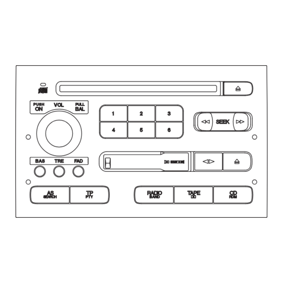
FX-M2017ZSA 8. OPERATIONS AND SPECIFICATIONS 8.1 OPERATIONS - RADIO PRESET RECALL PRESET CH.MEMORY POWER ON/OFF VOLUME MANUAL SEEK BALANCE BASS TREBLE FADER RADIO AUTO STORE BAND - TAPE POWER ON/OFF REWIND/FAST FORWARD VOLUME AUTO PROGRAM SEARCH BALANCE BLANK SKIP TAPE EJECT BASS DIRECTION TREBLE... -
Page 81: Specifications
FX-M2017ZSA - CD CD EJECT DISC SELECT (MULTI CD) POWER ON/OFF VOLUME TRACK UP/DOWN BALANCE REVERSE/FAST FORWARD MANUAL/SEEK CHANGE BASS TREBLE FADER RANDOM SINGLE/MULTI SELECT 8.2 SPECIFICATIONS Power source.............13.5V±0.1V TAPE Grounding system........Negative type Tape ........Compact cassette tape(C30-C90) Tape speed ..4.76 cm/sec.(+0.14 cm/sec.,-0.05 cm/sec.) Dimensions ....195.6(W) 118.2(H) 183.5(D)mm...
Need help?
Do you have a question about the FX-M2017ZSA X1B and is the answer not in the manual?
Questions and answers