Sony PCM-D50 Service Manual
Linear pcm recorder
Hide thumbs
Also See for PCM-D50:
- Service manual (78 pages) ,
- Operating instructions manual (60 pages) ,
- Specifications (2 pages)

Related Manuals for Sony PCM-D50


Summary of Contents for Sony PCM-D50
- Page 1 PCM-D50 SERVICE MANUAL US Model Canadian Model Ver. 1.3 2008.05 AEP Model E Model SPECIFICATIONS LINEAR PCM RECORDER Sony Corporation 9-887-869-04 2008E04-1 Audio Business Group © 2008.05 Published by Sony Techno Create Corporation...
- Page 3 ON THE SCHEMATIC DIAGRAMS AND IN PIÈCES SONT CRITIQUES POUR LA SÉCURITÉ DE FONC- THE PARTS LIST ARE CRITICAL TO SAFE OPERATION. TIONNEMENT. NE REMPLACER CES COM- POSANTS QUE PAR DES PIÈCES SONY DONT LES NUMÉROS SONT DON- REPLACE THESE COMPONENTS...
-
Page 4: Table Of Contents
PCM-D50 TABLE OF CONTENTS GENERAL ..............DISASSEMBLY 2-1. Panel (Front) Assy ............11 2-2. Ornamental Belt (Upper) Assy ........11 2-3. Backlight Board .............. 12 2-4. Power Board ..............12 2-5. REC VOL Assy, HP VOL Assy ........13 2-6. DA Board ................ 13 2-7. -
Page 5: General
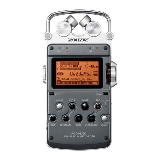
PCM-D50 SECTION 1 This section is extracted GENERAL from instruction manual. Identifying parts and controls Front Right side... - Page 6 PCM-D50 Built-in microphones (page 21) DIVIDE button (page 35) Peak level lamps (L/R) (page 24) PLAY/ENTER button/indicator Displays left and right peak levels of an (pages 31) audio signal input with -12dB (green) and STOP button (pages 25, 32) OVER (red) lamps.
- Page 7 PCM-D50 Identifying parts and controls (continued) Left side LIMITER switch (pages 22, 43) LOW CUT FILTER switch (pages 22, 43) Hole for attaching the tripod (not supplied) INPUT switch (pages 23, 28, 29, 30) When set to “ ” (microphone), records an...
- Page 8 PCM-D50 Display Time information Each time the DISPLAY button is pressed, the time information changes as follows (Flashes when the recorder is paused): Elapsed recording/playback time Remaining recordable time of the current memory (During playback: Remaining time of the current track)
- Page 9 PCM-D50 Identifying parts and controls (continued) Memory Stick indicator Displayed when the current memory is a “Memory Stick.” Folder number, track numbers Folders are classified into (a folder for recording and playback) and (a folder for playback only) (page 38). Track numbers are displayed as “current track number/total...
-
Page 10: Disassembly
PCM-D50 SECTION 2 DISASSEMBLY 2-1. PANEL (FRONT) ASSY (Page 11) 2-2. ORNAMENTAL BELT (UPPER) ASSY (Page 11) 2-3. BACKLIGHT BOARD 2-4. POWER BOARD (Page 12) (Page 12) 2-5. REC VOL ASSY, HP VOL ASSY (Page 13) 2-6. DA BOARD (Page 13) 2-7. -
Page 11: Panel (Front) Assy
PCM-D50 Note: 2-1. PANEL (FRONT) ASSY two screws (M 1.7) two cushions (panel) panel (front) assy two cushions (panel) two screws (M 1.7) 2-2. ORNAMENTAL BELT (UPPER) ASSY screw guard (MC) (M 1.4) ornamental belt (upper) assy two screws (M 1.4) screw (M 1.4) -
Page 12: Backlight Board
PCM-D50 2-3. BACKLIGHT BOARD two claws LCD assy BACKLIGHT board LCD unit (13 core) (CN4201) two screws P2 lock ace (M 1.7) Remove the two solders. white LCD assy two screws P2 lock ace (M 1.7) 2-4. POWER BOARD Remove the four solders. -
Page 13: Rec Vol Assy, Hp Vol Assy
PCM-D50 2-5. REC VOL ASSY, HP VOL ASSY Remove the six solders. white knob (VOL) orange yellow gray black HP VOL assy two screws precision pan (M 1.4) (EG) REC VOL assy CN3001 guard (VOL) screw 2-6. DA BOARD chassis (PWB) -
Page 14: Ad Board, Mic001, Mic002
PCM-D50 2-7. AD BOARD, MIC001, MIC002 MIC001 MIC002 Remove the six solders. MIC001 MIC002 black yellow yellow black two screws P2 lock ace (M 1.7) S3002 S3003 AD board screw (M2 grip) ground plate Remove the two solders. screw (M 1.7) 2-8. -
Page 15: Test Mode
PCM-D50 SECTION 3 TEST MODE 5. Flow Chart of the TEST MODE START 1. Setting and Exiting the TEST MODE After power-on, idle or sleep state LIMITER SW OFF Press [A-B]+[DIVIDE] at the same time LIMITER SW ON 2. Initial State of the TEST MODE and Exiting Method... - Page 16 PCM-D50 SERVICE MODE DSP Loop Version Key Check Lcd Contrast fi Display the current UI value. Display the key confirmed. Count down the number of the remaining keys. fi Cluster Num Key Chk+Format RTC Interrupt fi Battery Display the key confirmed.
- Page 17 PCM-D50 DCIN LCD Contrast Adjustment <DCIN> A/D : 84h DETECT : OK [STOP/MENU] : RET fi VBUS – DA BOARD (Side A) – VLCD DGND <VBUS> C4202 DETECT (5T735) : OK S4202 DETECT (M66592) : OK [STOP/MENU] : RET CN4201...
-
Page 18: Diagrams
PCM-D50 SECTION 4 DIAGRAMS THIS NOTE IS COMMON FOR PRINTED WIRING BOARDS AND SCHEMATIC DIAGRAMS. (In addition to this, the necessary note is printed in each block.) For Printed Wiring Boards. For Schematic Diagrams. Note: Note: • • All capacitors are in F unless otherwise noted. (p: pF) : Parts extracted from the component side. -
Page 34: Schematic Diagram - System Section (1/5)
GPIO PowerSW... - Page 45 PCM-D50 • IC Block Diagrams IC3001 ADA4841-2YRZ-R7 (AD Board (1/3)) IC3002 AD8662ARZ-REEL (AD Board (1/3)) IC3003 AD8662ARZ-REEL (AD Board (1/3)) IC3004 AD8662ARZ-REEL (AD Board (1/3)) IC4002 AD8662ARZ-REEL (DA Board) IC4004 AD8662ARZ-REEL (DA Board) OUTA –INA OUTB –INB +INA V– +INB...
- Page 46 PCM-D50 IC3401 NJU6366AF1(TE1) (AD Board (2/3)) 3-STATE BUFFER IC3403 NJU6311RB2(TE1) (AD Board (2/3)) 3-STATE OUTPUT SELECTOR BUFFER...
- Page 47 PCM-D50 IC3404 AK4114VQ-L (AD Board (2/3)) 48 47 46 45 44 43 42 41 40 39 38 CLOCK ERROR & IPS0/RX4 36 INT0 RECOVERY STATUS AVSS DETECT DIF0/RX5 TEST2 DIAF DIF1/RX6 DECODER AVSS 35 OCKS0/CSN/CAD0 AC_3/MPEG DIF2/RX7 34 OCKS1/CCLK/SCL DETECT...
- Page 48 PCM-D50 IC4005 AK4385ET-E2 (DA Board) 16 DZFL 15 DZFR 14 VDD 13 VCC MCLK 12 AOUTL+ INTERPOLATOR MODULATOR 11 AOUTL- BICK AUDIO DATA SDTI INTERFACE LRCK 10 AOUTR+ INTERPOLATOR MODULATOR 9 AOUTR- DE-EMPHASIS CLOCK SMUTE/CSN CONTROL DIVIDER ACKS/CCLK INTERFACE DIFD/CDTI...
- Page 49 PCM-D50 IC4202 TK11150CSCL-G (DA Board) IC4203 TK11150CSCL-G (DA Board) OVER HEAT & OVER CURRENT PROTECTION CONTROL CIRCUIT BANDGAP REFERENCE IC1401 LMC7101BIM5X (SYSTEM Board (3/5)) 4 IN–...
- Page 50 PCM-D50 IC2303 XC6215S01XNR (POWER Board (4/4)) IC1501 XC6215B312GR (SYSTEM Board (4/5)) IC1502 XC6215B312GR (SYSTEM Board (4/5)) 4 VIN ON/OFF EACH CONTROL CIRCUIT CURRENT LIMIT 3 VOUT ERROR AMP VOLTAGE REFERENCE IC2002 XC61CN6002NR (POWER Board (1/4)) VOUT VREF 3 NC...
- Page 51 PCM-D50 IC2003 XC61CC5002NR (POWER Board (1/4)) IC2005 XC61CC3602NR (POWER Board (1/4)) VOUT VREF 3 NC IC2101 XC9303B093KR (POWER Board (2/4)) SYNCHRONOUS EXT1 8 EXT2 BLANK LOGIC 7 GND ERROR AMP COMPARATOR PWM/PFM CONTROLLER RAMP WAVE VREF=0.9V GENERATOR 6 FB 5 NC...
- Page 52 PCM-D50 IC2102 XC9505B093AR (POWER Board (2/4)) PWM/PFM PWM/PFM EXT1 10 EXT2 CONTROLLER CONTROLLER COMPARATOR COMPARATOR 9 GND ERROR AMP ERROR AMP 8 FB2 RAMP WAVE RAMP WAVE GENERATOR GENERATOR PWM1 7 PWM2 VREF1=0.9V VREF2=0.9V 6 EN2 IC2103 XC9226A336MR (POWER Board (2/4))
- Page 53 PCM-D50 • IC Pin Function Description SYSTEM BOARD (1/5) IC1001 MC-10051F1-FAE-A (SYSTEM CONTROL/DSP) Pin No. Pin Name Description — A1, A2, A3 Not used (Open) NAND_WEZ Write enable signal output to the NAND ROM — IO_B Power supply (VDD_GP1) —...
- Page 54 PCM-D50 Pin No. Pin Name Description — SWADP Not used (Open) — CAPVBDL Not used (Open) — VCCVBAT1 Power supply (battery) — USBTEST3 Not used (Open) — IO_A Power supply (VDD_GP1) AB0_A5 Address signal output to the USB I/F —...
- Page 55 PCM-D50 Pin No. Pin Name Description — ISENS Not used (Open) — DGND Ground — DISCHGVBUS Not used (Pull Down) — SESSV Not used (Open) — IDGD Not used (Open) — IO_B Power supply (VDD_GP1) AB0_CSZ2 Chip select signal output (Not used in this set)
- Page 56 PCM-D50 Pin No. Pin Name Description — LCD_ENABLE Not used (Open) — LCD_VSYNC Not used (Open) — CHGGND2 Ground — Not used (Open) SDR_DATA23 LED drive signal output SDR_DATA22 LED drive signal output SDR_DATA21 LED drive signal output — SDR_DATA20...
- Page 57 PCM-D50 Pin No. Pin Name Description — Ground — R22, R23 LCD_R2, LCD_R4_ Not used (Open) — GNDSINK Ground — VDD_L0 Power supply (VDD_L0) — VUSB Not used (Open) SDR_CKE0 Clock enable signal output to SD-RAM SDR_CSZ1 Chip select signal output (Not used in this set) (Open)
- Page 58 PCM-D50 Pin No. Pin Name Description W4, W5 SDR_A4, SDR_A3 Address signal output to SD-RAM SPI1_SO Serial data output to the digital audio I/F transceiver — Ground SPI1_CSZ0 Chip select signal output to the digital audio I/F transceiver — W11 to W18...
- Page 59 PCM-D50 Pin No. Pin Name Description — IO_C Power supply (VDD_GP1) AC10 CAM_YUV6 PWM signal output to the DC/DC converter AC11 CAM_YUV2 Power supply control signal output AC12 CAM_VS LINE OUT (OPT) transmitter power control signal output — AC13 ISENSE Not used (Open) —...
- Page 60 PCM-D50 Pin No. Pin Name Description — AE14 AVDD_LPLL Power supply (VDD_PLL) — AE15 AVDD_HPLL Power supply (VDD_PLL) — AE16 Ground AE17 DD1VFBK VDD_L1 power supply voltage feedback input — AE18 VDD_DSP Power supply (VDD_L1) — AE19 IO_A Power supply (VDD_IOA) —...
- Page 61 PCM-D50 SYSTEM BOARD (4/5) IC1503 M66592UG (USB I/F) Pin No. Pin Name Description — AFED33G Ground RST_N Reset signal input — DACK1_N/DSTB0_N Not used (Connected to VIF) — DEND0_N Not used (Open) CS_N Chip select signal input RD_N Read enable signal input —...
- Page 62 PCM-D50 Pin No. Pin Name Description MPBUS Bus mode signal input Address signal input Address signal input Date input/output D3/AD3 Date input/output D5/AD5 Date input/output Date input/output Date input/output...
- Page 63 PCM-D50 POWER BOARD (4/4) IC2301 UPD78F0501AMC-5A4-E2-A (SIRCS CONTROL) Pin No. Pin Name Description ANI1/P21 Sircs key signal output ANI0/P20 Sircs key signal output P01/TI010/TO00 Sircs key signal output P00/TI000 Sircs key signal output P120/INTP0/EXLVI Sircs signal input nRESET System reset signal input...
-
Page 64: Exploded Views 5-1. Front Panel Section
fi fi fi fi Ref. No. Part No. Description Remark Ref. No. Part No. Description Remark A-1361-514-A PANEL (FRONT) ASSY 3-254-149-01 SCREW (M1.7) 3-273-829-01 CUSHION (PANEL) -
Page 65: Lcd Section
PCM-D50 5-2. LCD SECTION LCD1... -
Page 66: Vol Section
Ref. No. Part No. Description Remark Ref. No. Part No. Description Remark 3-268-199-01 GUARD (VOL) A-1361-502-A DA BOARD, COMPLETE (US,CND,E) 3-225-996-11 SCREW (M1.4) (EG), PRECISION PAN A-1361-503-A DA BOARD, COMPLETE (AEP) 3-268-190-01 KNOB (REC VOL) 3-989-735-71 SCREW (M1.7), LOCK ACE, P2 3-273-783-01 KNOB (REC VOL) (B) A-1361-510-A... -
Page 67: Mic Section
Ref. No. Part No. Description Remark Ref. No. Part No. Description Remark 3-254-149-01 SCREW (M1.7) X-2188-307-1 SYSTEM BOARD ASSY (AEP,E) 3-268-196-01 HOLDER (TERMINAL) A-1362-386-A AD BOARD, COMPLETE 3-270-458-01 SPRING, CONTACT BH1401 1-251-928-21 SOCKET, BATTERY (for ML621) 3-254-082-01 SCREW BT1401 1-756-134-12 BATTERY, STORAGE, LITHIUM ION (ML621) 3-269-482-01 GUIDE (CONNECTOR) -
Page 68: Rear Panel Section
Ref. No. Part No. Description Remark Ref. No. Part No. Description Remark 3-268-188-01 KNOB (LIMITER) 3-270-466-01 SHAFT (STRAP) 3-268-178-11 PANEL (REAR) (US) 3-268-186-01 KNOB (POWER) 3-268-178-31 PANEL (REAR) (CND,AEP,E) 3-268-187-01 PLATE, KNOB FIXED 3-270-464-01 FOOT (REAR) 3-271-241-01 HOLDER (DPC KNOB) 3-989-735-71 SCREW (M1.7), LOCK ACE, P2 3-268-189-01... -
Page 69: Electrical Parts List
fi fi fi fi fl fi fi fi Ref. No. Part No. Description Remark Ref. No. Part No. Description Remark A-1362-386-A AD BOARD, COMPLETE C3054 1-117-919-11 TANTAL. CHIP 10uF 6.3V C3055 1-117-919-11 TANTAL. CHIP 10uF 6.3V ******************* C3056 1-100-381-11 ELECT CHIP 10uF <... - Page 70 Ref. No. Part No. Description Remark Ref. No. Part No. Description Remark CN3304 1-779-666-21 CONNECTOR, BOARD TO BOARD 40P < RESISTOR > < DIODE > R3001 1-245-816-11 METAL CHIP 2.2K 0.5% 1/10W R3002 1-216-864-11 SHORT CHIP D3005 8-719-069-29 DIODE RB520S-30TE61 R3003 1-218-990-81 SHORT CHIP...
- Page 71 Ref. No. Part No. Description Remark Ref. No. Part No. Description Remark R3098 1-218-990-81 SHORT CHIP R3412 1-218-990-81 SHORT CHIP R3099 1-218-990-81 SHORT CHIP R3414 1-218-929-11 RES-CHIP 1/16W R3100 1-218-990-81 SHORT CHIP R3415 1-218-990-81 SHORT CHIP R3101 1-218-990-81 SHORT CHIP R3417 1-218-990-81 SHORT CHIP...
- Page 72 Ref. No. Part No. Description Remark Ref. No. Part No. Description Remark C4011 1-125-837-11 CERAMIC CHIP 1uF 6.3V IC4203 6-705-337-01 IC TK11150CSCL-G C4013 1-135-646-11 FILM CHIP IC4204 6-711-822-01 IC TK77335AM4 C4014 1-135-646-11 FILM CHIP C4027 1-125-777-11 CERAMIC CHIP 0.1uF < JACK > C4050 1-117-919-11 TANTAL.
- Page 73 Ref. No. Part No. Description Remark Ref. No. Part No. Description Remark R4039 1-216-864-11 SHORT CHIP R4251 1-218-990-81 SHORT CHIP R4040 1-216-864-11 SHORT CHIP R4042 1-245-852-11 METAL CHIP 0.5% 1/10W < SWITCH > R4044 1-216-864-11 SHORT CHIP R4045 1-245-844-11 METAL CHIP 4.7K 0.5% 1/10W...
- Page 74 PCM-D50 POWER When IC2301 on the Power board are damaged, exchange the new Power board for the Power board which IC damaged.
- Page 75 Ref. No. Part No. Description Remark Ref. No. Part No. Description Remark R2209 1-218-949-11 RES-CHIP 1/16W S2212 1-786-157-31 SWITCH, TACTILE ( A-B) R2210 1-218-965-11 RES-CHIP 1/16W S2213 1-572-922-11 SWITCH, SLIDE (DPC) R2211 1-218-965-11 RES-CHIP 1/16W R2212 1-218-965-11 RES-CHIP 1/16W < THERMISTOR (POSITIVE) > R2213 1-218-953-11 RES-CHIP...
- Page 76 PCM-D50 SYSTEM When IC1001, IC1201, IC1301 and IC1503 on the System board are damaged, exchange the new System board for the System board which IC damaged.
- Page 77 Ref. No. Part No. Description Remark R1505 1-218-989-11 RES-CHIP 1/16W R1506 1-218-989-11 RES-CHIP 1/16W R1508 1-218-990-81 SHORT CHIP R1509 1-218-990-81 SHORT CHIP R1510 1-218-977-11 RES-CHIP 100K 1/16W R1511 1-218-977-11 RES-CHIP 100K 1/16W R1512 1-218-977-11 RES-CHIP 100K 1/16W R1513 1-218-990-81 SHORT CHIP R1601 1-218-990-81 SHORT CHIP...
- Page 78 Checking the version allows you to jump to the revised page. Also, clicking the version at the top of the revised page allows you to jump to the next revised page. 2007.10 2008.03 E model addition. 2008.04 AEP model addition. 2008.05 AD BOARD, COMPLETE is changed to the repair parts.