Sony CDX-R5515X Service Manual
Fm/am compact disc player fm/mw/lw compact disc player
Hide thumbs
Also See for CDX-R5515X:
- Operating instructions manual (36 pages) ,
- Installation/connections (2 pages) ,
- Operating & installation instructions (2 pages)
Table of Contents
Advertisement
CDX-R5515X/R5610/R6550
SERVICE MANUAL
Ver. 1.1 2005.07
• The tuner and CD sections have no adjustments.
AUDIO POWER SPECIFICATIONS (US MODEL)
POWER OUTPUT AND TOTAL HARMONIC DISTORTION
23.2 watts per channel minimum continuous average power into
4 ohms, 4 channels driven from 20 Hz to 20 kHz with no more
than 5% total harmonic distortion.
CD player section
Signal-to-noise ratio
120 dB
Frequency response
10 – 20,000 Hz
Wow and flutter
Below measurable limit
Tuner section
FM
Tuning range
CDX-R5515X:
87.5 – 107.9 MHz
CDX-R5610:
87.5 – 108.0 MHz (at 50 kHz step)
87.5 – 107.9 MHz (at 200 kHz step)
CDX-R6550:
87.5 – 108 MHz
Antenna terminal
External antenna connector
Intermediate frequency 10.7 MHz/450 kHz
Usable sensitivity
9 dBf
Selectivity
75 dB at 400 kHz
Signal-to-noise ratio
67 dB (stereo),
69 dB (mono)
Harmonic distortion at 1 kHz
0.5% (stereo),
0.3% (mono)
Separation
35 dB at 1 kHz
Frequency response
30 – 15,000 Hz
AM (CDX-R5515X)
Tuning range
530 – 1,710 kHz
Antenna terminal
External antenna connector
Intermediate frequency 10.7 MHz/450 kHz
Sensitivity
30 µV
Sony Corporation
9-879-368-02
2005G04-1
e Vehicle Group
© 2005.07
Published by Sony Engineering Corporation
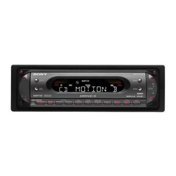
Photo: CDX-R6550
Model Name Using Similar Mechanism
CD Drive Mechanism Type
Optical Pick-up Name
SPECIFICATIONS
AM (CDX-R5610)
Tuning range
AM tuning interval
Aerial terminal
Intermediate frequency 10.7 MHz/450 kHz
Sensitivity
MW/LW (CDX-R6550)
Tuning range
Antenna terminal
Intermediate frequency 10.7 MHz/450 kHz
Sensitivity
Power amplifier section
Outputs
Speaker impedance
Maximum power output 52 W × 4 (at 4 ohms) (CDX-R5515X/R5610)
FM/AM COMPACT DISC PLAYER
FM/MW/LW COMPACT DISC PLAYER
US Model
Canadian Model
CDX-R5515X
AEP Model
UK Model
E Model
NEW
MG-611TA-186//K
KSS1000E
531 – 1,602 kHz (at 9 kHz step)
530 – 1,710 kHz (at 10 kHz step)
9 kHz/10 kHz switchable
External aerial connector
30 µV
MW: 531 – 1,602 kHz
LW: 153 – 279 kHz
External antenna connector
MW: 30 µV
LW: 40 µV
Speaker outputs
(sure seal connectors)
4 – 8 ohms
50 W × 4 (at 4 ohms) (CDX-R6550)
– Continued on next page –
CDX-R5515X/R5610
CDX-R6550
CDX-R5610
CDX-R6550
1
Advertisement
Table of Contents

Related Manuals for Sony CDX-R5515X


Summary of Contents for Sony CDX-R5515X
- Page 1 Speaker impedance 4 – 8 ohms 69 dB (mono) Harmonic distortion at 1 kHz Maximum power output 52 W × 4 (at 4 ohms) (CDX-R5515X/R5610) 50 W × 4 (at 4 ohms) (CDX-R6550) 0.5% (stereo), 0.3% (mono) – Continued on next page –...
-
Page 2: Service Notes
Card remote commander RM-X151 US and foreign patents licensed from Dolby Laboratories. Note This unit cannot be connected to a digital preamplifier or an equalizer which is Sony BUS system compatible. Design and specifications are subject to change without notice. - Page 3 CDX-R5515X/R5610/R6550 • CD Playback: UNLEADED SOLDER You can play CD-DA (also containing CD TEXT* ), CD-R/CD- Boards requiring use of unleaded solder are printed with the lead RW (MP3 files also containing Multi Session and ATRAC CD free mark (LF) indicating the solder contains no lead.
-
Page 4: Table Of Contents
CDX-R5515X/R5610/R6550 TABLE OF CONTENTS 1. GENERAL Location of Controls ..............5 Connections ................6 2. DISASSEMBLY 2-1. Sub Panel (LCD) Assy ............12 2-2. CD Mechanism Block ............12 2-3. Main Board ............... 13 2-4. Chassis (T) Sub Assy ............13 2-5. -
Page 5: General
SECTION 1 GENERAL This section is extracted from instruction manual. • LOCATION OF CONTROLS • CDX-R5515X Location of controls and basic operations G DSO button 2 The following buttons on the card remote Main unit commander have also different buttons/functions To select the DSO mode (1, 2, 3 or OFF). -
Page 6: Connections
To select PTY in RDS; list up. CUSTOM or OFF). R Receptor for the card remote commander • CONNECTIONS • CDX-R5515X Connection example (2) Notes (2- A ) • Be sure to connect the ground lead before connecting the amplifi er. -
Page 7: Connection Example
CDX-R5515X/R5610/R6550 • CDX-R5610 • CDX-R6550 Connection example (2) Notes (2- A ) • Be sure to connect the earth lead before connecting the amplifi er. • The alarm will only sound if the built-in amplifi er is used. AUDIO OUT FRONT... - Page 8 CDX-R5515X/R5610/R6550 • CDX-R5515X Source selector (not supplied) Supplied with the CD/MD changer Sélecteur de source Fourni avec le changeur de CD/MD (non fourni) XA-C30 Supplied with XA-C30 Fourni avec le XA-C30 AUDIO OUT REMOTE FRONT BUS AUDIO IN from car antenna à...
- Page 9 CDX-R5515X/R5610/R6550 • CDX-R5610...
- Page 10 CDX-R5515X/R5610/R6550 • CDX-R6550 Supplied with XA-C30 Note for the aerial connecting Remarque sur le raccordement de Opmerking bij de antenne-aansluiting If your car aerial is an ISO (International l’antenne Indien uw auto is uitgerust met een Mit dem XA-C30 geliefert...
-
Page 11: Disassembly
CDX-R5515X/R5610/R6550 SECTION 2 DISASSEMBLY Note : This set can be disassemble according to the following sequence. 2-1. SUB PANEL (LCD) ASSY (Page 12) 2-2. CD MECHANISM BLOCK (Page 12) 2-10. SERVO BOARD 2-4. CHASSIS (T) SUB ASSY 2-3. MAIN BOARD... -
Page 12: Sub Panel (Lcd) Assy
CDX-R5515X/R5610/R6550 Note : Follow the disassembly procedure in the numerical order given. 2-1. SUB PANEL (LCD) ASSY 3 two claws 2 two claws 1 two screws (+PTT 2.6 x 6) 4 sub panel (LCD) assy 2-2. CD MECHANISM BLOCK 7 bracket (CD) -
Page 13: Main Board
CDX-R5515X/R5610/R6550 2-3. MAIN BOARD 1 three screws (+BTT) 2 two screws (+PTT 2.6 x 8) 3 MAIN board 4 insulating sheet 2-4. CHASSIS (T) SUB ASSY 4 claw 2 two screws (+P 1.7 x 2.2) 1 two screws (+P 1.7 x 2.2) -
Page 14: Roller Arm Assy
CDX-R5515X/R5610/R6550 2-5. ROLLER ARM ASSY 3 washer (1.1-2.5) 5 roller arm assy 4 gear (RA1) 2 spring (RAR) 1 spring (RAL) 2-6. CHASSIS (OP) ASSY qa chassis (OP) assy 0 coil spring (damper) lever (D) 4 washer 1 CN2 (16P) -
Page 15: Optical Pick-Up
CDX-R5515X/R5610/R6550 2-7. OPTICAL PICK-UP 2 chucking arm sub assy 5 claw 1 tension coil spring (CHKG) 7 optical pick-up 6 main shaft 4 rack (SL) 3 screw (+B 1.4 x 5) 2-8. SL MOTOR ASSY (M902) 1 screw (+P 1.4 x 1.8) -
Page 16: Le Motor Assy (M903)
CDX-R5515X/R5610/R6550 2-9. LE MOTOR ASSY (M903) 8 screw 0 gear (LE) assy (+M 1.7 x 2.5) 9 bearing (LEB-N) 2 washer qa screw (+M 1.7 x 2.5) qf two toothed lock screws 3 gear (LE1) (+M 1.4 ) lever (D) -
Page 17: Front Back Panel (Lcd)
CDX-R5515X/R5610/R6550 2-11. FRONT BACK PANEL (LCD) 2 two screws (+P 2 x 8) three claws two claws 1 two screws (+P 2 x 8) two claws three claws 3 front back panel (LCD) 2-12. KEY BOARD 2 CN903 (6P) 4 KEY board... -
Page 18: Display Section
CDX-R5515X/R5610/R6550 2-13. DISPLAY SECTION Note for assembly 4 display section After installing to the front panel assy, make sure the spring is not off from the dowel. 2 two screws (+P 2 x 8) Note for assembly After installing to the front panel assy, make sure the spring is not off from the dowel. -
Page 19: Spring (S)
CDX-R5515X/R5610/R6550 2-15. SPRING (S) 5 spring (S) display (SV) assy Note for assembly 3 Take off the spring from display (SV) assy the dowel on preset assy side. 4 spring (S) dowel spring (S) preset assy 1 Raise the preset assy up in the arrowed direction. - Page 20 CDX-R5515X/R5610/R6550 MEMO...
-
Page 21: Diagrams
CDX-R5515X/R5610/R6550 SECTION 3 DIAGRAMS 3-1. BLOCK DIAGRAM — CD SECTION — • R-ch is omitted due to same as L-ch. • Signal Path : CD PLAY DETECTOR MAIN FPI2 RFEQO 77 RFI 85 AGCI CD-L SECTION 78 RFRPI 86 RFDCI... -
Page 22: Block Diagram -Main Section
CDX-R5515X/R5610/R6550 3-2. BLOCK DIAGRAM — MAIN SECTION — J451 (1/3) ELECTRONIC VOLUME FRONT IC401 AUDIO OUT R-CH CD-L 9 SE1L J451 (2/3) SECTION OUT LR2 (Page 21) R-CH 10 SE1R REAR OUT RR2 R-CH AUDIO OUT R-CH J451 (3/3) POWER AMP,... -
Page 23: Block Diagram -Display Section
CDX-R5515X/R5610/R6550 3-3. BLOCK DIAGRAM — DISPLAY SECTION — SYSTEM CONTROL LCD DRIVER IC501 (3/3) IC901 KEY MATRIX KEYIN0 LSW903-913,918-921 LCD SO S902,914-918 KEYIN1 3-28, LCD911 LCD CKO 30-64, LIQUID D501 (1/2) LCD CE CRYSTAL DISPLAY COM1 KEY ACK ON PANEL... -
Page 24: Circuit Boards Location
CDX-R5515X/R5610/R6550 3-4. CIRCUIT BOARDS LOCATION • NOTE FOR PRINTED WIRING BOARDS AND SCHEMATIC DIAGRAMS THIS NOTE IS COMMON FOR PRINTED WIRING BOARDS AND SCHEMATIC DIAGRAMS. (In addition to this, the necessary note is printed in each block.) SERVO board SENSOR board For schematic diagrams. -
Page 25: Printed Wiring Boards -Cd Mechanism Section
CDX-R5515X/R5610/R6550 3-5. PRINTED WIRING BOARDS — CD MECHANISM SECTION — • Refer to page 24 for Circuit Boards Location. : Uses unleaded solder. 1-864-900- 1-864-900- • Semiconductor Location Ref. No. Location MAIN BOARD CN350 (Page 28) B-11 CDX-R5515X/R5610/R6550... -
Page 26: Schematic Diagram -Cd Mechanism Section (1/2)
CDX-R5515X/R5610/R6550 • Refer to page 24 for Waveforms. 3-6. SCHEMATIC DIAGRAM — CD MECHANISM SECTION (1/2) — • Refer to page 36 for IC Block Diagrams. IC B/D C102 TP25 TP26 TP27 TP93 TP29 R125 R126 R127 R128 R113 TP101... -
Page 27: Schematic Diagram -Cd Mechanism Section (2/2)
CDX-R5515X/R5610/R6550 • Refer to page 24 for Waveform. • Refer to page 36 for IC Block Diagram. 3-7. SCHEMATIC DIAGRAM — CD MECHANISM SECTION (2/2) — • Refer to page 38 for IC Pin Description. (Page 26) (Page 30) TP88... -
Page 28: Printed Wiring Board -Main Section
CDX-R5515X/R5610/R6550 3-8. PRINTED WIRING BOARD — MAIN SECTION — • Refer to page 24 for Circuit Boards Location. : Uses unleaded solder. J451 JC302 CNJ400 (ANTENNA) J451 CN300 C323 C414 C442 C422 C324 JW134 C432 C307 C305 C309 R452 JW133... -
Page 29: Schematic Diagram -Main Section (1/2)
CDX-R5515X/R5610/R6550 • Refer to page 24 for Waveform. 3-9. SCHEMATIC DIAGRAM — MAIN SECTION (1/2) — • Refer to page 36 for IC Block Diagram. C303 J451 JC302 C308 C306 C323 C324 JC300 JC301 C309 C304 C301 C305 C307 C443 R443... -
Page 30: Schematic Diagram -Main Section (2/2)
CDX-R5515X/R5610/R6550 • Refer to page 24 for Waveforms. 3-10. SCHEMATIC DIAGRAM — MAIN SECTION (2/2) — • Refer to page 40 for IC Pin Description. (Page 29) L303 J370 L302 L301 D501 JC508 R550 (Page 27) R529 R528 R538 D493... -
Page 31: Printed Wiring Board -Key Section
CDX-R5515X/R5610/R6550 3-11. PRINTED WIRING BOARD — KEY SECTION — • Refer to page 24 for Circuit Boards Location. : Uses unleaded solder. LED914 LED902 S914,LED914 S902,LED902 S915 S917 S917,LED917 S915,LED915 S902 S914 VOL+ (Page 35) (Page 33) PRESET BOARD DISPLAY BOARD... -
Page 32: Schematic Diagram -Key Section
CDX-R5515X/R5610/R6550 3-12. SCHEMATIC DIAGRAM — KEY SECTION — D902 CN901 LED902 LED914 R973 CN902 R974 R948 R943 LED917 LED915 R976 JP942 R949 R944 (Page 30) R972 (Page 34) IC972 R950 JP941 R945 R975 C973 LED918 LED916 R951 R946 S961 CN903... -
Page 33: Printed Wiring Board -Display Section
CDX-R5515X/R5610/R6550 3-13. PRINTED WIRING BOARD — DISPLAY SECTION — • Refer to page 24 for Circuit Boards Location. : Uses unleaded solder. LED931 (LCD BACK LIGHT) LSW901 LSW901 LSW921 LSW918 LSW918 LSW921 R953 DSPL R920 LCD911 LIQUID CRYSTAL DISPLAY PANEL... -
Page 34: Schematic Diagram -Display Section
CDX-R5515X/R5610/R6550 3-14. SCHEMATIC DIAGRAM — DISPLAY SECTION — LED931 R960 R953 LED961 CN904 R964 R961 LSW921(2/2) R924 LSW918(2/2) R965 R954 R925 R966 R962 R955 R926 (Page 32) R983 LED932 LSW919(2/2) IC901 LSW920(2/2) C982 C981 LSW901(2/2) C983 C984 C985 R969 Q925... -
Page 35: Printed Wiring Board -Preset Section
CDX-R5515X/R5610/R6550 3-15. PRINTED WIRING BOARD — PRESET SECTION — • Refer to page 24 for Circuit Boards Location. : Uses unleaded solder. LSW903 LSW905 LSW906 LSW910 LSW904 LSW907 LSW908 LSW909 LSW911 LSW912 LSW913 1-864-699- LSW903 LSW904 LSW905 LSW906 LSW907 LSW908... - Page 36 CDX-R5515X/R5610/R6550 • IC BLOCK DIAGRAMS IC2 TC94A60MFG-301 (SERVO Board (1/2)) IC1 BA5968FP-E2 (SERVO Board (2/2)) IC300 TDA8588AJ/N2/R1 (MAIN Board (1/2)) 72 71 66 65 64 63 62 61 60 59 58 56 55 54 53 52 51 OPIN4+ LDCTL OUT FL-...
- Page 37 CDX-R5515X/R5610/R6550 IC401 TDA7419TR (MAIN Board (1/2)) ACOUTR ACINR ACINL SUBWOOFER L.P.F ACOUTL BUSS OUTRR2 MIDDLE VREF SAOUT SPECTRUM ANALYZER SAIN AC2INL AC2INR TREBLE SOFTSTEP VOLUME SOFT MUTE LOUDNESS MUTE OUTLF OUTLR1 OUTRR1 OUTRF IN GAIN OUTLR2 AUTO ZERO SE2L SUPPLY...
- Page 38 CDX-R5515X/R5610/R6550 • IC PIN DESCRIPTIONS • IC3 MB90487APFV-G-131-BNDE1 (CD SYSTEM CONTROL) (SERVO BOARD (2/2)) Pin No. Pin Name Pin Description Servo 1.5 V power supply control signal output 2 to 6 — Not used. (Open) CD BUS0 Bus data signal input/output 0...
- Page 39 CDX-R5515X/R5610/R6550 Pin No. Pin Name Pin Description XUART Sony-Bus/MC-Bus change signal input H: Sony-Bus, L: MC-Bus ZMUTE Zero detection mute signal output MECON CHK MECON rising detection signal input CDON CHK CDON rising detection signal input 69 to 74 —...
- Page 40 CDX-R5515X/R5610/R6550 • IC501 MB90488BPF-G-119-BNDE1 (SYSTEM CONTROL) (MAIN BOARD (2/2)) Pin No. Pin Name Pin Description AREA SEL2 Destination setting pin AREA SEL1 Destination setting pin AREA SEL0 Destination setting pin Not used BEEP Beep signal output Not used NOSE SW...
- Page 41 Back-up power supply detect signal input Not used DAVN RDS data block synchronized detect signal input Not used UNI SI SONY bus data input UNI SO SONY bus data output UNI SCK SONY bus clock output Not used Not used...
-
Page 42: Exploded Views
CDX-R5515X/R5610/R6550 SECTION 4 EXPLODED VIEWS NOTE: • The mechanical parts with no reference • Color Indication of Appearance Parts The components identified by mark 0 or dotted line with mark number in the exploded views are not supplied. Example : 0 are critical for safety. -
Page 43: Front Panel Section
CDX-R5515X/R5610/R6550 4-2. FRONT PANEL SECTION not supplied not supplied (KEY board) LCD901 not supplied supplied not supplied not supplied (DISPLAY board) 61 62 not supplied not supplied not supplied (PRESET board) not supplied not supplied not supplied not supplied Ref. No. -
Page 44: Cd Mechanism Section (1)
CDX-R5515X/R5610/R6550 4-3. CD MECHANISM SECTION (1) (MG-611TA-186//K) not supplied (SENSOR board) not supplied not supplied not supplied not supplied Ref. No. Part No. Description Remark Ref. No. Part No. Description Remark A-3372-455-A CHASSIS (T) SUB ASSY 3-253-748-01 DAMPER (S) 3-253-729-01 SPRING (LTR), TENSION COIL 3-352-758-31 SCREW (M1.7), TOOTHED LOCK... -
Page 45: Cd Mechanism Section (2)
CDX-R5515X/R5610/R6550 4-4. CD MECHANISM SECTION (2) (MG-611TA-186//K) (including M901) M902 not supplied not supplied not supplied not supplied The components identified by Les composants identifiés par mark 0 or dotted line with mark une marque 0 sont critiques 0 are critical for safety. -
Page 46: Cd Mechanism Section (3)
CDX-R5515X/R5610/R6550 4-5. CD MECHANISM SECTION (3) (MG-611TA-186//K) M903 Ref. No. Part No. Description Remark Ref. No. Part No. Description Remark 3-262-755-01 WASHER (1.1-2.5) 2-186-696-11 BRACKET (LEM-N) 2-186-699-11 GEAR (RA1) 3-345-648-91 SCREW (M1.4), TOOTHED LOCK A-1075-789-A ARM ASSY, ROLLER A-1083-637-A GEAR (LE) ASSY... -
Page 47: Cd Mechanism Section (4)
CDX-R5515X/R5610/R6550 4-6. CD MECHANISM SECTION (4) (MG-611TA-186//K) Ref. No. Part No. Description Remark Ref. No. Part No. Description Remark 2-186-700-11 GEAR (CHK1) 3-899-829-01 WASHER (SLIT) 3-344-223-01 WASHER 3-259-032-01 GEAR (LE2) 3-259-470-01 GEAR (LE1) A-1075-791-A CHASSIS (M) BLOCK ASSY 3-253-755-02 LEVER (D) -
Page 48: Electrical Parts List
CDX-R5515X/R5610/R6550 SECTION 5 DISPLAY ELECTRICAL PARTS LIST NOTE: • Due to standardization, replacements in • Items marked “*” are not stocked since The components identified by mark 0 or dotted line with mark the parts list may be different from the they are seldom required for routine service. -
Page 49: Display Key
CDX-R5515X/R5610/R6550 DISPLAY Ref. No. Part No. Description Remark Ref. No. Part No. Description Remark R969 1-216-817-11 METAL CHIP 1/10W R902 1-216-819-11 METAL CHIP 1/10W (R5515X) R913 1-216-819-11 METAL CHIP 1/10W R980 1-216-809-11 METAL CHIP 1/10W R914 1-216-819-11 METAL CHIP 1/10W... - Page 50 CDX-R5515X/R5610/R6550 MAIN Ref. No. Part No. Description Remark Ref. No. Part No. Description Remark A-1084-640-A MAIN BOARD, COMPLETE (R6550) C315 1-162-970-11 CERAMIC CHIP 0.01uF A-1085-702-A MAIN BOARD, COMPLETE (R5610) C316 1-104-665-11 ELECT 100uF A-1085-863-A MAIN BOARD, COMPLETE (R5515X) C317 1-126-961-11 ELECT 2.2uF...
- Page 51 CDX-R5515X/R5610/R6550 MAIN Ref. No. Part No. Description Remark Ref. No. Part No. Description Remark C472 1-107-823-11 CERAMIC CHIP 0.47uF D304 6-500-522-01 DIODE 10EDB40-TA1B2 C480 1-136-154-00 FILM 0.012uF D305 6-500-522-01 DIODE 10EDB40-TA1B2 C481 1-136-154-00 FILM 0.012uF D306 6-500-522-01 DIODE 10EDB40-TA1B2 C482 1-162-965-11 CERAMIC CHIP 0.0015uF 10%...
- Page 52 CDX-R5515X/R5610/R6550 MAIN Ref. No. Part No. Description Remark Ref. No. Part No. Description Remark JC350 1-216-296-11 SHORT CHIP < RESISTOR > JC360 1-216-864-11 SHORT CHIP JC420 1-216-864-11 SHORT CHIP 1-216-809-11 METAL CHIP 1/10W JC430 1-216-296-11 SHORT CHIP (R6550) JC490 1-216-296-11 SHORT CHIP...
- Page 53 CDX-R5515X/R5610/R6550 MAIN Ref. No. Part No. Description Remark Ref. No. Part No. Description Remark R451 1-216-809-11 METAL CHIP 1/10W R537 1-216-845-11 METAL CHIP 100K 1/10W R452 1-216-841-11 METAL CHIP 1/10W R538 1-216-864-11 SHORT CHIP 0 (R5515X/R5610) R460 1-216-809-11 METAL CHIP...
- Page 54 CDX-R5515X/R5610/R6550 PRESET SENSOR Ref. No. Part No. Description Remark Ref. No. Part No. Description Remark PRESET BOARD R908 1-216-827-11 METAL CHIP 3.3K 1/10W R909 1-216-829-11 METAL CHIP 4.7K 1/10W ************* R910 1-218-867-11 METAL CHIP 6.8K 0.5% 1/10W < CONNECTOR >...
- Page 55 CDX-R5515X/R5610/R6550 SERVO Ref. No. Part No. Description Remark Ref. No. Part No. Description Remark A-1075-784-A SERVO BOARD, COMPLETE C106 1-125-777-11 CERAMIC CHIP 0.1uF ********************** < CONNECTOR > < CAPACITOR > 1-691-380-21 CONNECTOR, FFC/FPC 16P 1-100-567-81 CERAMIC CHIP 0.01uF 1-817-275-21 CONNECTOR, BOARD TO BOARD 28P 1-125-777-11 CERAMIC CHIP 0.1uF...
- Page 56 CDX-R5515X/R5610/R6550 SERVO Ref. No. Part No. Description Remark Ref. No. Part No. Description Remark 1-218-945-11 RES-CHIP 1/16W 1-795-561-21 VIBRATOR, CERAMIC (16.9344MHz) 1-218-941-81 RES-CHIP 1/16W ************************************************************* 1-218-941-81 RES-CHIP 1/16W 1-218-977-11 RES-CHIP 100K 1/16W MISCELLANEOUS 1-218-941-81 RES-CHIP 1/16W *************** 1-218-941-81 RES-CHIP 1/16W...
- Page 57 CDX-R5515X/R5610/R6550 Ref. No. Part No. Description Remark ACCESSORIES ************ 1-479-077-11 REMOTE COMMANDER (RM-X151) 2-348-439-11 MANUAL, INSTRUCTION (ENGLISH,FRENCH) (R5515X) 2-348-439-21 MANUAL, INSTRUCTION (ENGLISH,GERMAN, FRENCH,ITALIAN,DUTCH) (R6550) 2-348-439-31 MANUAL, INSTRUCTION (ENGLISH,SPANISH, TRADITIONAL CHINESE) (R5610) 2-348-440-11 MANUAL, INSTRUCTION, INSTALL (ENGLISH, FRENCH) (R5515X) 2-348-440-21 MANUAL, INSTRUCTION, INSTALL (ENGLISH,...
- Page 58 CDX-R5515X/R5610/R6550 MEMO...
- Page 59 CDX-R5515X/R5610/R6550 US Model Canadian Model CDX-R5515X SERVICE MANUAL AEP Model UK Model Ver. 1.1 2005.07 CDX-R6550 E Model CDX-R5610 SUPPLEMENT-1 File this supplement with the service manual. Subject : Change of CD mechanism. This model provides two types of CD mechanisms.
- Page 60 CDX-R5515X/R5610/R6550 EXPLODED VIEWS NOTE: • The mechanical parts with no reference • Color Indication of Appearance Parts The components identified by mark 0 or dotted line with mark number in the exploded views are not supplied. Example : 0 are critical for safety.
- Page 61 CDX-R5515X/R5610/R6550 2. CD MECHANISM SECTION (2) (MG-611TA-186//C) (including M901) M902 not supplied not supplied Ref. No. Part No. Description Remark Ref. No. Part No. Description Remark A-1088-612-A CHASSIS (OP) COMPLETE ASSY 3-261-959-21 SPRING (SL), TORSION 3-316-938-91 SCREW (B1.4X5), TAPPING 3-253-736-21 SPRING (CHKG), TENSION...
- Page 62 CDX-R5515X/R5610/R6550 3. CD MECHANISM SECTION (3) (MG-611TA-186//C) M903 Ref. No. Part No. Description Remark Ref. No. Part No. Description Remark 3-262-755-11 WASHER (1.1-2.5) 2-186-696-21 BRACKET (LEM-N) 2-186-699-21 GEAR (RA1) 3-345-648-91 SCREW (M1.4), TOOTHED LOCK A-1088-618-A ARM ASSY, ROLLER A-1088-623-A GEAR (LE) ASSY...
- Page 63 CDX-R5515X/R5610/R6550 4. CD MECHANISM SECTION (4) (MG-611TA-186//C) Ref. No. Part No. Description Remark Ref. No. Part No. Description Remark 2-186-700-21 GEAR (CHK1) 3-899-829-01 WASHER (SLIT) 3-344-223-01 WASHER 2-590-545-21 GEAR (LE2-M) 3-259-470-22 GEAR (LE1) A-1088-620-A CHASSIS (M) BLOCK ASSY 3-253-755-21 LEVER (D)
- Page 64 CDX-R5515X/R5610/R6550 REVISION HISTORY Clicking the version allows you to jump to the revised page. Also, clicking the version at the upper on the revised page allows you to jump to the next revised page. Ver. Date Description of Revision 2004.12 2005.07...
Need help?
Do you have a question about the CDX-R5515X and is the answer not in the manual?
Questions and answers