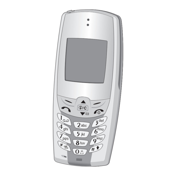
LG G5300 Service Manual

Gsm phone
Hide thumbs Also See for G5300:
Table of Contents

Advertisement

Quick Links

GSM Phone
SERVICE MANUAL
MODEL : G5300 / W5300
P/N : MMBD0020301
DECEMBER, 2002

Advertisement

Table of Contents
loading

Summary of Contents for LG G5300

  • Page 1 GSM Phone SERVICE MANUAL MODEL : G5300 / W5300 P/N : MMBD0020301 DECEMBER, 2002...
  • Page 2: Table Of Contents

    Table Of Contents 3.11 Display and Interface ......42 1. INTRODUCTION ........3.12 Keypad Switches and Scanning ..43 1.1 Purpose ..........3 3.13 Microphone ........44 1.2 Regulatory Information ......3 3.14 Earpiece ..........45 A. Security ..........3 3.15 Hands-free Interface ......
  • Page 3 7. BLOCK DIAGRAM ......112 11. STAND ALONE TEST ....123 11.1 Introduction ........123 8. CIRCUIT DIAGRAM ......113 A. Tx Test .......... 123 B. Rx Test .......... 123 8.1 MAIN ..........113 11.2 Setting Method ......123 8.2 MEMORY & MMI ......114 A.
  • Page 4: Introduction

    1. INTRODUCTION 1. INTRODUCTION 1.1 Purpose This manual provides the information necessary to repair, calibration, description and download the features of this model. 1.2 Regulatory Information A. Security Toll fraud, the unauthorized use of telecommunications system by an unauthorized part (for example, persons other than your company’s employees, agents, subcontractors, or person working on your company’s behalf) can result in substantial additional charges for your telecommunications services.
  • Page 5: Notice Of Radiated Emissions

    1. INTRODUCTION E. Notice of Radiated Emissions This model complies with rules regarding radiation and radio frequency emission as defined by local regulatory agencies. In accordance with these agencies, you may be required to provide information such as the following to the end user. F.
  • Page 6: Abbreviations

    1. INTRODUCTION 1.3 Abbreviations For the purposes of this manual, following abbreviations apply: Automatic Power Control Baseband Bit Error Ratio CC-CV Constant Current – Constant Voltage Digital to Analog Converter Digital Communication System dB relative to 1 milliwatt Digital Signal Processing EEPROM Electrical Erasable Programmable Read-Only Memory Electrostatic Discharge...
  • Page 7: Performance

    2. PERFORMANCE 2. PERFORMANCE 2.1 H/W Features Item Feature Comment Li-ion, 850 mAh Standard Battery Si e: 42.73 64.25 7.5mm Weight: 30g Under the minimum current consumption environment Stand by Current (such as paging period 9), the level of standby current is below 4mA.
  • Page 8: Technical Specification

    2. PERFORMANCE 2.2 Technical Specification Item Description Specification TX: 890 + n 0.2 MHz RX: 935 + n 0.2 MHz (n = 1 ~ 124) EGSM Frequency Band TX: 890 + (n – 1024) 0.2 MHz RX: 935 + (n – 1024) 0.2 MHz (n = 975 ~ 1024) TX: 1710 + (n –...
  • Page 9 2. PERFORMANCE Item Description Specification GSM, EGSM Offset from Carrier (kHz). Max. dBc +0.5 600 ~ 1,200 1,200 ~ 1,800 1,800 ~ 3,000 3,000 ~ 6,000 Output RF Spectrum 6,000 (due to modulation) Offset from Carrier (kHz). Max. dBc +0.5 600 ~ 1,200 1,200 ~...
  • Page 10 2. PERFORMANCE Item Description Specification GSM, EGSM BER (Class II) < 2.439% @-102 dBm Bit Error Ratio BER (Class II) < 2.439% @-100 dBm RX Level Report Accuracy 3 dB 8 3 dB Frequency (Hz) Max.(dB) Min.(dB) Sending Response 1,000 2,000 3,000 3,400...
  • Page 11 2. PERFORMANCE Item Description Specification 32.768KHz tolerance ≤ 30 ppm At least 80 dB under below conditions: Ringer Volume 1. Ringer set as ringer. 2. Test distance set as 50 cm Fast Charge : < 500 mA Charge Voltage Slow Charge: < 60 mA Antenna Bar Number Power -85 dBm ~...
  • Page 12: Technical Brief

    3. TECHNICAL BRIEF 3. TECHNICAL BRIEF 3.1 General Description The RF parts consists of a transmitter part, a receiver part, a synthesizer part, a voltage supply part, a VCTCXO part. And the main RF Chipset CX74017[U401] is a single-chip dual-band transceiver for the extended global system for mobile communication[E-GSM900MHz]/Digital communication system[DCS1800MHz] voice and data transfer applications.
  • Page 13: Rf Front End

    3. TECHNICAL BRIEF A. RF front end RF front end consists of Antenna Switch(FL401), dual band LNAs integrated in transceiver(U401). The Received RF signals (GSM 925MHz ~ 960MHz, DCS 1805MHz ~ 1880MHz) are fed into the antenna or mobile switch. An antenna matching circuit is between the antenna and the mobile switch.
  • Page 14: Transmitter Part

    3. TECHNICAL BRIEF 3.3 Transmitter Part The Transmitter part contains CX74017 active parts, PAM and Antenna Switch. The CX74017 active part consists of a vector modulator and offset phase-locked loop block(OPLL) including down- converter, phase detector, loop filter and dual band transmit VCO which can operate at either final RF output frequency.
  • Page 15: Opll

    3. TECHNICAL BRIEF B. OPLL The offset mixer down converts the feedback Tx RF signal using LO to generate a IF modulating signal. The IF signal goes via external passive bandpass filter to one port of the phase detector. The other side of the phase detector input is LO signal.
  • Page 16: Power Amplifier

    3. TECHNICAL BRIEF The counter and mode settings of the synthesizer are also programmed via 3-wire interface. Figure 3-3. Synthesizer Block diagram. D. Power Amplifier The RF3110[U402] is a Dual band amplifier for E-GSM(880 to 915MHz) and DCS1800(1710 to 1785MHz). The efficiency of module is the 50% at nominal output power for E-GSM and the 45% for DCS1800.
  • Page 17: 13 Mhz Clock

    3. TECHNICAL BRIEF 3.4 13 MHz Clock The 13 MHz clock (X401) consists of a TCXO (Temperature Compensated Crystal Oscillator) which oscillates at a frequency of 13 MHz. It is used within the CX74017 RF Main Chip, BB Analog chip-set (AD6521), and Digital (AD6522). 2V7_VTCXO C454 2.2u...
  • Page 18: Testing Set-Up And Checking Signals

    3. TECHNICAL BRIEF 3.6 Testing Set-up and Checking Signals A. Received RF Level and Checks This section shows the typical RF levels expected throughout the receiver path. A block diagram showing the locations of the RF measurement points and levels is shown in Fig. 3-11. Receiver Testing Set-up To check the receiver the following conditions have to be set: On a signal generator or a GSM/DCS test box, output a CW signal of amplitude = -60 dBm at either:...
  • Page 19 3. TECHNICAL BRIEF Testing Transmitter Using a suitable high frequency probe measure the RF levels at the relevant points shown in Fig. 3-9, 10, and compare your measurements with those shown in the diagram. If there are any major difference between the readings taken and those indicated then further investigation of that particular point will be required.
  • Page 20 3. TECHNICAL BRIEF RF components (Component Side) CN401 FL401 FL402 U402 U401 U404 U403 X401 Figure 3-6. RF components (Component Side). Reference Description Reference Description U401 RF Main Chipset FL402 Dual SAW Filter CN401 Mobile S/W X401 VCTCXO FL401 Ant. S/W U404 U402 U403...
  • Page 21 3. TECHNICAL BRIEF Test point of Rx Levels Figure 3-7. Test point of Rx Levels. - 20 -...
  • Page 22 3. TECHNICAL BRIEF Test point of TX Levels Figure 3-8. Test point of TX Levels (1). - 21 -...
  • Page 23 3. TECHNICAL BRIEF Control signal test points (1) TX RAMP TXPA 2.85V 13MHz CLOCK VTCXO RXIQ TXIQ Figure 3-9. Control signal test points (1). - 22 -...
  • Page 24 3. TECHNICAL BRIEF Control signal test points (2) TP403 (RX EN) TP406 (PLL DATA) TP402 (PLL LE) TP404 (PLL CLK) Figure 3-10. Control signal test points (2). - 23 -...
  • Page 25 3. TECHNICAL BRIEF Figure 3-11. Transmitter & Receiver RF Levels. - 24 -...
  • Page 26 3. TECHNICAL BRIEF Figure 3-12. Regulator Output (RF2V8). Figure 3-13. VCTCXO Power Supply (2V7_VTCXO). - 25 -...
  • Page 27 3. TECHNICAL BRIEF Figure 3-14. 13MHz Clock. Figure 3-15. Control Signal of FEM in Rx mode (GSM, DCS both). - 26 -...
  • Page 28 3. TECHNICAL BRIEF Figure 3-16. Control Signal of FEM in GSM TX mode. Figure 3-17. Control Signal of FEM in DCS TX mode. - 27 -...
  • Page 29 3. TECHNICAL BRIEF Figure 3-18. PLL_LE, PLL_CLK, PLL_DATA. Figure 3-19. TX_EN, TA_RAMP, TXPA. - 28 -...
  • Page 30 3. TECHNICAL BRIEF Figure 3-20. TX IQ Signal. TXIP TXQN Figure 3-21. RX IQ Signal. - 29 -...
  • Page 31: Digital Main Processor

    3. TECHNICAL BRIEF 3.7 Digital Main Processor The AD6522 is an ADI designed processor. Figure 3-22. Top level block diagram of the AD6522 internal architecture. BUS Arbitration Subsystem It is to work as a cross point for data accesses between the three main buses. EBUS is for external accesses, primarily from Flash memory for code and data.
  • Page 32 3. TECHNICAL BRIEF MCU subsystem It consists of an ARM7TDMI central processing unit, a boot ROM, a clock generation and access control module. The maximum clock frequency for the ARM7TDMI is 39MHz at 2.45V. The main clock is 13MHz and it is provided by VCTCXO. The Clock & BS(Bus Select) generator make internal clock by multiplying the main clock by 1X, 1.5X, 2X and 3X.
  • Page 33 3. TECHNICAL BRIEF AD6522 GSM-PROCESSOR JTAGEN KEYPADCOL[4:0] KEYPAD TCK. TMS KEYPADROW[4:0] JTAG Matrix TDI. TDO Backlight BACKLIGHT0 JTAGE. HSL.GPIO Service light Universal BACKLIGHT1 USCTX/RX/CLK System Generic Serial port A Connector Generic Serial port B (USC) Generic Serial port D ROMCS FLASH ADD[23:0] 16 bit...
  • Page 34 3. TECHNICAL BRIEF Interconnection with external devices RTC block interface Countered by external X-TAL The X-TAL oscillates 32.768KHz LCD module interface Mainly controlled by _LCD_MAIN_CS, LCD_RES, LCD_RS, _WR, DATA [00...15] signals. Table 3-3. Description _LCD_MAIN_CS LCD driver chip enable. LCD driver IC has own CS pin LCD_RES This pin resets LCD module.
  • Page 35 3. TECHNICAL BRIEF SIM interface The AD6522 check status periodically in call mode if SIM card is inserted or not, but the AD6522 don't check in deep sleep mode. Interface by SIMDATAOP, SIMCLK, SIM_RST(GPIO_23) Table 3-5. Description This pin receives and sends data to SIM card. This model supports only SIMDATAOP 3.0 volt interface SIM card.
  • Page 36: Analog Main Processor

    3. TECHNICAL BRIEF 3.8 Analog Main Processor AD6521 AD6521 MCLK Dual-Mode Voiceband B aseband Code c JTAG Interface MCLKEN RESET for ICO ITXP I TRANSMIT INTERP FILTER ITXN BSDI QTXP Q TRANSMIT FILTER QTXN BSIFS GMSK MOD BSAEBAND 32 x 10 bit TXON SERIAL 10 bit...
  • Page 37 3. TECHNICAL BRIEF BB Transmit section This section generates in-phase and quadrature BB modulated GMSK signals (BT = 0.3) in accordance with GSM 05.05 Phase 2 specifications. The transmit channel consists of a digital GMSK modulator, a matched pair of 10-bit DACs and a matched pair of reconstruction filter.
  • Page 38 3. TECHNICAL BRIEF 3V0_VLCD R220 2.2K 3V0_VLCD C225 3V0_VLCD R221 C224 10uF 3.3K (2012) R222 U206 MAX9075EXK-T VIN- HEADSET_MIC_P HOOK_DETECT VIN+ 3V0_VLCD R233 510K U205 C232 MAX4695EGC 0.1u C233 R235 N_C2 N_C1 0.1u AUXIP GOM1 GOM2 AUXIN R237 2.2K HFK_AUXIN HFK_AUXIP HFK_EAR HFK_EAR...
  • Page 39 3. TECHNICAL BRIEF CN202 VOUTNORP C203 VOUTNORN C206 C207 CLOSE TO RECEIVER Figure 3-26-2. Voice band circuit diagram. 2V45_VAN R202 C202 C204 10uF R204 (2012) (2012) 1.2K C208 0.1u R206 VINNORP MIC201 C209 C210 C211 0.1u R208 VINNORN C213 R211 1.2K R213 Q203...
  • Page 40 3. TECHNICAL BRIEF 2V45_VAN 2V45_VCORE R101 AUXADC4 MVBAT TO U102_#A4 C116 220n R102 100K C141 C117 C118 C119 C120 C121 C122 TXIP ITXP ITXN TXIN QTXN TXQN QTXP TXQP IRXP RXIP 2V8_VMEM RXON IRXN RXIN TXON QRXP RXQP QRXN RXQN MCLK MCLKEN R108...
  • Page 41: Power Management

    3. TECHNICAL BRIEF 3.9 Power management Figure 3-28. ADP3408 inner block diagram. Table 3-6. Description VSIM 2.86 V (is provided to SIM card) VCORE 2.45 V (is provided to the AD6522 & AD6521’s digital core) VRTC 2.45 V (is provided to the RTC and Backup Battery) 2.45 V (is provided to the AD6521 I/O and used as microphone bias) VTCXO 2.715 V (is provided to VCTCXO)
  • Page 42 3. TECHNICAL BRIEF Power up sequence logic The ADP3408 controls power on sequence. Power on sequence If a battery is inserted, the battery powers the 6 LDOs. Then if PWRONKEY is detected, the LDOs output turn on. REFOUT is also enabled, Reset is generated and send to the AD6522. LDO block There are 6 LDOs in the ADP3408.
  • Page 43: Memories

    3. TECHNICAL BRIEF 3.10 Memories 128Mbit flash memory + 32Mbit PSRAM 16 bit parallel data bus ADD01 ~ ADD22. 2 Chip enables for Flash memory select. RF Calibration data, Audio parameters and battery calibration data etc are stored in Flash memory area.
  • Page 44: Keypad Switches And Scanning

    3. TECHNICAL BRIEF 3.12 Keypad Switches and Scanning The key switches are metal domes, which make contact between two concentric pads on the keypad layer of the PCB when pressed. There are 19 switches (S301-S325, not used S303~S309), connected in a matrix of 5 rows by 5 columns, as shown in Figure, except for the power switch (S310), which is connected independently.
  • Page 45: Microphone

    3. TECHNICAL BRIEF 3.13 Microphone The microphone is placed to the front cover and contacted to main PCB. The audio signal is passed to VINNORP (#J10) and VINNORN (#K10) pins of AD6522. The voltage supply 2V45_VAN is output from ADP3408, and is a bias voltage for both the VINNORP (through R101) and VINAUX (through R112) lines.
  • Page 46: Earpiece

    3. TECHNICAL BRIEF 3.14 Earpiece The earpiece is driven directly from AD6521 VOUTNORP (#K8) and VOUTNORN (#K7) pins and the gain is controlled by the PGA in an AD6521. The earpiece is placed in the front cover and contacted to main PCB. CN202 VOUTNORP C203...
  • Page 47: Key Back-Light Illumination

    3. TECHNICAL BRIEF 3.17 Key Back-light Illumination In key back-light illumination, there are 12 Blue LEDs in Main Board, which are driven by KEY_BACKLIGHT line from AD6522. VBAT KEY BACKLIGHT C227 C228 C229 C230 C231 LD201 LD202 LD203 LD204 LD205 LD206 Q202 IMX9T110...
  • Page 48: Lcd Back-Light Illumination

    3. TECHNICAL BRIEF 3.18 LCD Back-light Illumination In LCD Back-light illumination, there is a driver in FPCB of LCD Board, which is driven by BACKLIGHT line from AD6522. VBAT LCD BACKLIGHT 0.1u C205 U201 MAX4599EXT-T Q204 IMX9T110 BACKLIGHT R228 5 COM R220 NC 4 VCHARGE...
  • Page 49: Speaker & Midi Ic

    3. TECHNICAL BRIEF 3.19 Speaker & MIDI IC The phones of this model don’t use buzzer, but uses the loud speaker and Melody IC which makes the robust joyful melody sounds. Melody IC control 5 GPIO is assigned to control melody IC. Melody data is transferred to melody IC and played by loud phone.
  • Page 50 3. TECHNICAL BRIEF Basically, this phone have a melody IC of Yamaha Ltd.MA-2(nickname from Yamaha) is a synthesizer LSI for mobile phones that realize advanced game sounds. This LSI has a built-in speaker amplifier, and thus, is an ideal device for outputting sounds that are used by mobile phones in addition to game sounds and ringing melodies that are replayed by a synthesizer.
  • Page 51: Trouble Shooting

    4. TROUBLE SHOOTING 4. TROUBLE SHOOTING 4.1 RF Components CN401 FL401 FL402 U402 U401 U404 U413 X401 RF Components Reference Description Reference Description U401 RF Main Chipset FL402 Dual SAW Filter CN401 Mobile S/W X401 VCTCXO FL401 Ant. S/W U404 U402 U403 Inverter IC...
  • Page 52: Rx Trouble

    4. TROUBLE SHOOTING 4.2 Rx Trouble START HP8922 : Test mode 62 CH, 7 level setting (TCH) 62 CH, - 60dBm setting (BCCH) Spectrum analyzer setting Ocillo scop e setting 1. Check Regulator Circuit 2. Check VCTCXO Circuit 3. Check Control RX Check Area Signal...
  • Page 53 4. TROUBLE SHOOTING 4-2-1 Checking Regulator Circuit U404.1 U404.6 RF2.85V VBAT U404 VSYNTHEN _ERR C458 R430 10uF C457 ADP3330 2.2u 2012 C459 2012 470p Check Pin 6. RF 2.85V O.K ? Check Pin 1. Pin 6. High ? Changing the Board Regulat or Circuit is OK.
  • Page 54 4. TROUBLE SHOOTING 4-2-2 Checking VCTCXO Circuit X401. 4 X401. 3 2V7_VTCXO C454 2.2u X401 2012 U403 13MHz SN74AHC1GU04DCKR C457 C455 R424 1000p R425 13MHZ 1000p R426 Graph 4-1. VCTCXO 13MHz Graph 4-2. VCTCXO 2.7V - 53 -...
  • Page 55 4. TROUBLE SHOOTING 4-2-3 Checking Control Signal TP402 (LE) TP403 (REXN) Data Clock TP404 (Clock) TP406 (Data) Graph 4-3. RF Control Signal Lev el is H igh? Download the SW Check TP 403. Check TP 406, 404, 402. Check if there is Download the SW Similar? Any Major Difference...
  • Page 56 4. TROUBLE SHOOTING 4-2-4 Checking Ant SW & Mobile SW CN401 PIN 2 CN401 PIN 1 L420 C448 C445 L410 L409 FL401 Table 4-1. ANT SW Control Logic - 55 -...
  • Page 57 4. TROUBLE SHOOTING CN 401 KMS-502 Graph 4-4. ANT SW Control GSM. DCS RX Mode RX_EN DCSSEL High GSMSEL TXPA Graph 4-5. Dual Control Signal for GSM RX Mode ANT SW GSMSEL DCSSEL TXPA RX_EN EGSM TX DCSSEL DCS TX High EGSM RX GSMSEL...
  • Page 58 4. TROUBLE SHOOTING 4-2-5 Checking Saw Filter Circuit L408 10nH L409 L410 2.7nH 1.8nH C444 1.2p FL402 FAR-G6CS-1G8425-L257 L411 OUT1 3.3nH 3 IN2 OUT2 C450 0.5p C451 C452 1.5p FL406.3 FL406.1 FL402.5 FL402.7 - 57 -...
  • Page 59 4. TROUBLE SHOOTING 2-6 Checking RX IQ RXIN RXQN RXIP RXQP Graph 4-7. RX IQ Signal Graph 4-8. RX I Signal (Extended) - 58 -...
  • Page 60: Tx Trouble

    4. TROUBLE SHOOTING 4.3 Tx Trouble - 59 -...
  • Page 61 4. TROUBLE SHOOTING 4-3-1 Checking Regulator Circuit • If you already check this point while checking RX part, You can skip this test. U404. 1 U404. 2 U404. 6 RF2.85V VBAT U404 VSYNTHEN _ERR C458 R430 10uF C457 ADP3330 2.2u 2012 C459 2012...
  • Page 62 4. TROUBLE SHOOTING 4-3-2 Checking VCTCXO Circuit • If you already check this point while checking RX part, you can skip this test. X401.4 X401.3 2V7_VTCXO C454 2.2u X401 2012 13MHz U403 SN74AHC1GU04DCKR C457 C455 R424 1000p R425 13MHZ 1000p R426 Graph 4-9.
  • Page 63 4. TROUBLE SHOOTING 4-3-3 Checking Control Signal TX_EN PLL_LE TXRAMP PLL_DATA PLL_CLK TXPA Graph 4-11. RF Control Signal Graph 4-12. TXEN, TXRAMP, TXPA TP 409(LE) TP404 (RXEN) TXEN (TP402) TXRAMP (R401) TXPA (R404) TP408(Clock) TP407(Data) - 62 -...
  • Page 64 4. TROUBLE SHOOTING 4-3-4 Checking TX IQ C449 C453 RXIN TXQN RXIP TXQP Graph 4-13. TX IQ Signal - 63 -...
  • Page 65 4. TROUBLE SHOOTING 4-3-5 Checking RF TX Level R406 L405 R401 L402 R403 L401 R404 R405 C427 U402 U401 R414 C427 - 64 -...
  • Page 66 4. TROUBLE SHOOTING 4-3-6 Checking Ant SW & Mobile SW CN401.1 C425 C448 FL401 C445 FL401.5 FL401.3 Table 4-3. ANT SW Control Logic - 65 -...
  • Page 67 4. TROUBLE SHOOTING High High Graph 4-14. ANT SW Control Graph 4-15. ANT SW Control DCS TX Mode GSM TX Mode TXEN TXEN DCSSEL High DCSSEL GSMSEL High GSMSEL TXPA TXPA High High Graph 4-16. Dual AND Gate input Graph 4-17. Dual AND Gate input For DCS TX Mode For DCS TX Mode Table 4-4.
  • Page 68 4. TROUBLE SHOOTING 4-3-7 Receiver and Transmitter RF Level - 67 -...
  • Page 69 4. TROUBLE SHOOTING 4-3-8 Receiver RF Level Figure 4-1. Test Points of Rx Level. - 68 -...
  • Page 70 4. TROUBLE SHOOTING 4-3-9 Transmitter RF Level Figure 4-2. Test Points of Tx Level. - 69 -...
  • Page 71 4. TROUBLE SHOOTING 4-3-10 Test Points for RF Components TX_RAMP TXPA RF 2.85V 2V7_VCTCXO 13 MHz Clock RX IQ TX IQ Figure 4-3. Test Points for RF components. - 70 -...
  • Page 72 4. TROUBLE SHOOTING 4-3-11 Test Points for RF Components TP403 (RX_EN) TP406 (PLL_DATA) TP404 (PLL_LE) TP404 (PLL_CLK) Figure 4-4. Test Points for RF components (Keypad Side/Lower). - 71 -...
  • Page 73: Power On Trouble

    4. TROUBLE SHOOTING 4.4 Power On Trouble SETTING : Connect PIF, and set remote switch off at PIF. - 72 -...
  • Page 74 4. TROUBLE SHOOTING • Test) U301 (ADP3408) Check!! POWER-ON KEY R340 C329 signal input C330 0.1u 10uF _RESET C331 C332 (2012) 100p 100p VBAT These powers should be VCHARGE POWERKEY PWRONKEY ROWX KEYROW0 SIM_EN SIMEN necessary to power on. 2V85_VSIM C333 10uF MVBAT MVBAT...
  • Page 75: Charging Trouble

    4. TROUBLE SHOOTING 4.5 Charging Trouble SETTING : Connect the battery and the charging adaptor(TA) to the phone. - 74 -...
  • Page 76 4. TROUBLE SHOOTING • Test) Q301 & D302 Check!! R347 Q301 The charging current will flow into this direction. VBAT VCHARGE POWERKEY PWRONKEY SIM_EN SIMEN C333 10uF CHRIN (2012) ISENSE R347 VBAT 0.33 GATEDR C334 1000p BATSNS D302 Q301 CUS02 RESCAP C335 0.1u...
  • Page 77: Lcd Trouble

    4. TROUBLE SHOOTING 4.6 LCD Trouble - 76 -...
  • Page 78 4. TROUBLE SHOOTING • Test ) CN304 Check!! CN301 A) Check the connection between LCD & Main board B) Check the soldering of LCD & Main board C) Replace LCD module - 77 -...
  • Page 79: Receiver Trouble

    4. TROUBLE SHOOTING 4.7 Receiver Trouble SETTING : After Initialize Agilent 8960, Test in EGSM, DCS Mode - 78 -...
  • Page 80 4. TROUBLE SHOOTING • The Receiver part Circuit Diagram CN202 VOUTNORP C203 VOUTNORN C206 C207 CLOSE TO RECEIVER VA203 C207 C206 - 79 -...
  • Page 81: Speaker Trouble

    4. TROUBLE SHOOTING 4.8 Speaker Trouble SETTING : Connect PIF to the phone, and Power on. Enter The engineering mode, and set “Melody on” at Buzzer of BB test menu. - 80 -...
  • Page 82 4. TROUBLE SHOOTING • Test) Speaker Check!! CN201 U202 U207 The Power for analog part of the melody IC Circuit diagram VBAT 3V3_VMIDI U202 LP3981ILD-3.3 VOUT VMIDI_CTL BYPASS C220 2.2u VOUT_SE GND1 C221 HFK_EAR CONNECTION (2012) GND2 0.1u C222 HEADSET 4.7uF_2012 The Power for analog part of the melody IC The voltage is 3.3V...
  • Page 83 4. TROUBLE SHOOTING The Melody IC & Speaker part Circuit Diagram These 4 components make up the analog amplified stage of melody. R201 13MHz CLK1 HPOUT_R _MIDI_RST _RST C201 2V8_VMEM HPOUT_L R203 0.01u ADD0 _MIDI_CS R244 R205 _MIDI_IRQ _IRQ C205 R244 R212 390p...
  • Page 84: Mic. Trouble

    4. TROUBLE SHOOTING 4.9 Mic. Trouble SETTING : After Initialize Agilent 8960, Test in EGSM, DCS Mode. - 83 -...
  • Page 85 4. TROUBLE SHOOTING 2V45_VAN C204 R202 R202 C202 C204 The signal flow of 10uF R204 (2012) (2012) R204 the microphone to 1.2K R206, R208, U103. C206, C211 C208 0.1u R206 MIC201 VINNORP C209 C210 C211 0.1u R208 VINNORN C213 R211 1.2K R213 Q203...
  • Page 86 4. TROUBLE SHOOTING MIC201 C206 R208 C203 R202 R204 C114 C208 R206 - 85 -...
  • Page 87: Vibrator Trouble

    4. TROUBLE SHOOTING 4.10 Vibrator Trouble SETTING : After Initialize Agilent 8960, Test in EGSM, Connect PIF to the phone, and Power on. Enter The engineering mode, and set 'Vibrator on' at Vibration of BB test menu. - 86 -...
  • Page 88 4. TROUBLE SHOOTING D201 R217 Q201 R218 CN203 VIBRATOR VBAT When the vibrator works, the signal at this point goes to 2.8V CN203 C219 0.1u When the vibrator works, the R217 current flow this direction. R218 VIBRATOR Q201 1.5K 2SC5585 R219 When the vibrator works, 100K...
  • Page 89: Backlight Led Trouble

    4. TROUBLE SHOOTING 4.11 Backlight LED Trouble SETTING : Connect PIF to the phone, and power on. Enter engineering mode, and set “Backlight on” in “at” “BB test-Backlight” menu - 88 -...
  • Page 90 4. TROUBLE SHOOTING • Test) D302~D313/Diode & Q201 Check!! LD201 LD202 LD203 Q202 LD204 R234 R236 LD205 LD206 VBAT KEY BACKLIGHT C227 C228 C229 C230 C231 LD201 LD202 LD203 LD204 LD205 LD206 Q202 IMX9T110 R234 KEY_BACKLIGHT 1.5K R236 100K SP207 R238 R239 A) Check the diode LD201~LD206.
  • Page 91: Sim Detect Trouble

    4. TROUBLE SHOOTING 4.12 SIM Detect Trouble SETTING : Insert the SIM into J301. Connect PIF to the phone, and power on. - 90 -...
  • Page 92 4. TROUBLE SHOOTING • Test) SIM Connector Check!! J301 BACKLIGHT GPO_22 KEY_BACKLIGHT GPO_23 2V9_SIM 2V9_SIM PLL_PD GPIO_22 GPIO_23 R133 SIMEN GPIO_24 SIMCLK SIMDATAOP J101 R150 - 91 -...
  • Page 93: Earphone Trouble

    4. TROUBLE SHOOTING 4.13 Earphone Trouble SETTING : After Initialize Agilent 8960, Test in EGSM, DCS Mode. - 92 -...
  • Page 94 4. TROUBLE SHOOTING - 93 -...
  • Page 95 4. TROUBLE SHOOTING J201 R241 R240 L201 L234 - 94 -...
  • Page 96 4. TROUBLE SHOOTING U205 U204 U203 - 95 -...
  • Page 97 4. TROUBLE SHOOTING This part makes 3V0_VLCD the mic bias of the ear-mic. R220 The reference voltage for 2.2K 3V0_VLCD the hook-detect of ear-mic. C225 3V0_VLCD R221 C224 10uF 3.3K (2012) R222 U206 MAX9075EXK-T VIN- HEADSET_MIC_P HOOK_DETECT VIN+ The direction of the audio 3V0_VLCD R233 signal from the ear-mic.
  • Page 98: Hfk Trouble

    4. TROUBLE SHOOTING 4.14 HFK Trouble SETTING : After initializing GSM test equipment, Connect PIF to the phone, and power on. - 97 -...
  • Page 99 4. TROUBLE SHOOTING U205 CN302 - 98 -...
  • Page 100 4. TROUBLE SHOOTING 2V8_VMEM VBAT VCHARGE R327 R328 R329 R330 100K 100K 100K 100K CN302 CN302 R331 USC3 R332 USC0 R333 USC1 R334 USC2 R335 USC4 R336 USC5 R337 ACC_DET R338 R339 R341 HFK_AUXON R342 HFK_AUXOP R343 HFK_AUXIP R344 HFK_AUXIN R345 RPWRON R346...
  • Page 101: Disassembly Instruction

    5. DISASSEMBLY INSTRUCTION 5. DISASSEMBLY INSTRUCTION 5.1 Disassembly 1. Remove the Battery and Screws as shown below. Figure 5-1. Removing the Battery. 2. Lift up and remove the Rear cover. Figure 5-2. Removing the Rear cover. - 100 -...
  • Page 102 5. DISASSEMBLY INSTRUCTION 3. Detach the rest components as shown below. Figure 5-3. Detaching the rest components. - 101 -...
  • Page 103 5. DISASSEMBLY INSTRUCTION 4. First, lift up PCB and remove the Antenna holding the hooks of the both end sides. After that, detach the Receiver and Keypad. Figure 5-4. Removing PCB, Antenna, Receiver and Keypad. 5. Use a tweezers to remove the Battery locker and Spring. Figure 5-5.
  • Page 104: Download And Calibration

    6. DOWNLOAD AND CALIBRATION 6. DOWNLOAD AND CALIBRATION 6.1 Download A. Download Setup Figure 6-1 describes Download setup. Figure 6-1. Download Setup 2. Condition Disconnect TA to the Datakit and phone have a battery Check the battery up to two blocks more. - 103 -...
  • Page 105 6. DOWNLOAD AND CALIBRATION B. Download Procedure 1. Access Flash loader program in PC and select Erase. (Don’t check OWCD) 2. Check Address and Size (Address : 1004000, Size : 7FC000) - 104 -...
  • Page 106 6. DOWNLOAD AND CALIBRATION 3. Press Start and Wait until Erase is completed. 4. Change Address and Size (Address : 18000000, Size : 800000) - 105 -...
  • Page 107 6. DOWNLOAD AND CALIBRATION 5. Press Start and Wait until Erase is completed again. 6. Press Write to start Download. - 106 -...
  • Page 108 6. DOWNLOAD AND CALIBRATION 7. Select Key to choose software (Mot. File). 8. Select Mot.file and Press Open. - 107 -...
  • Page 109 6. DOWNLOAD AND CALIBRATION 9. Wait until converting from MOT to BIF is completed. ( Just check Verify. Don’t check OWCD ) 10. Press Start and Power on the phone using JIG remote Power on (Switch 1). Turn on Switch 1 REMOTE 11.
  • Page 110: Calibration

    6. DOWNLOAD AND CALIBRATION 6.2 Calibration A. Equipment List Table 6-1. Calibration Equipment List. Equipment for Calibration Type / Model Brand Wireless Communication Test Set HP-8960 Agilent RS-232 Cable and Test JIG RF Cable Power Supply HP-66311B Agilent GPIB interface card HP-GPIB Agilent Calibration &...
  • Page 111: Test Jig Operation

    6. DOWNLOAD AND CALIBRATION Figure 6-3. The top view of Test Jig. C. Test Jig Operation Table 6-2. Jig Power. Power Supply usually 4.0V DC Adaptor 9.5V, 500mA Table 6-3. Jig DIP Switch. Switch Number Name Description Switch 1 RPWRON In ON state, phone is awaked.
  • Page 112: Procedure

    6. DOWNLOAD AND CALIBRATION Table 6-4. LED Description. LED Number Name Description LED 1 Power Power is provided for Test Jig. LED 2 Indicate charging state of the phone battery LED 3 UART Indicate data transfer state through the UART port LED 4 Indicate data transfer state through the MON port 1.
  • Page 113: Block Diagram

    7. BLOCK DIAGRAM 7. BLOCK DIAGRAM Figure 7-1. block diagram. - 112 -...
  • Page 114: Circuit Diagram

    MODEL 12/02 SP110 Designer CS LEE 2002 J_VBAT J_GND KEYCOL0 Checked YK KIM DRAWING KEYCOL1 NAME NS KIM KEYCOL2 Approved KEYCOL3 KEYCOL4 DRAWING Iss. Notice No. Date Name LG Electronics Inc. VER 1.4 LGIC(42)-A-5505-10:01 LG Electronics Inc. - 113 -...
  • Page 115: Memory & Mmi

    SW KIM 2002 C234 10uF HEADSET_SPK_P JACK_DETECT YK KIM Checked HEADSET_MIC_P J201 L201 DRAWING 100nH C235 C236 C237 R241 NAME Approved NS KIM DRAWING Iss. Notice No. Date Name LG Electronics Inc. VER 1.4 LGIC(42)-A-5505-10:01 LG Electronics Inc. - 114 -...
  • Page 116: Midi

    Designer MK CHEN DAN222 2002 TP413 VBAT ONNOFF RPWRON YK KIM Checked PWRON DRAWING R349 200K NAME NS KIM Approved TP411 TP412 DRAWING Iss. Notice No. Date Name LG Electronics Inc. VER 1.4 LGIC(42)-A-5505-10:01 LG Electronics Inc. - 115 -...
  • Page 117: Rf Circuit

    DH KIM VSYNTHEN DRAWING TEMPSENSE _ERR RF Circuit C457 R430 NAME C458 2.2u NS KIM Approved 10uF ADP3330 2012 2012 C459 470p DRAWING Iss. Notice No. Date Name LG Electronics Inc. VER 1.4 LGIC(42)-A-5505-10:01 LG Electronics Inc. - 116 -...
  • Page 118: Pcb Layout

    9. PCB LAYOUT 9. PCB LAYOUT - 117 -...
  • Page 119 9. PCB LAYOUT - 118 -...
  • Page 120: Engineering Mode

    10. ENGINEERING MODE 10. ENGINEERING MODE A. About Engineering Mode Engineering mode is designed to allow a service man/engineer to view and test the basic functions provided by a handset. B. Access Codes The key sequence for switching the engineering mode on is 2945#*#. Pressing END will switch back to non-engineering mode operation.
  • Page 121: Adc (Analog To Digital Converter) [1-5]

    10. ENGINEERING MODE E. ADC (Analog to Digital Converter) [1-5] This displays the value of each ADC. • MVBAT ADC (Main Voltage Battery ADC) [1-5-1] • AUX ADC (Auxiliary ADC) [1-5-2] • TEMPER ADC (Temperature ADC) [1-5-3] F. BATTERY [1-6] •...
  • Page 122: Rf Test [Menu 2]

    10. ENGINEERING MODE 10.2 RF Test [MENU 2] Radio Frequency Test A. SAR Test [2-1] This menu is to test the Specific Absorption Rate. • SAR Test On [2-1-1] : Phone continuously process TX only. Call-setup equipment is not required. •...
  • Page 123: Trace Option [Menu 4]

    10. ENGINEERING MODE 10.4 Trace option [MENU 4] This is NOT a necessary menu to be used by neither engineers nor users. 10.5 Call Timer [MENU 5] A. All calls [5-1] This displays total conversation time. User cannot reset this value. B.
  • Page 124: Stand Alone Test

    11. STAND ALONE TEST 11. STAND ALONE TEST 11.1 Introduction This manual explains how to examine the status of RX and TX of the model. A. Tx Test TX test - this is to see if the transmitter of the phones is activating normally B.
  • Page 125: Means Of Test

    11. STAND ALONE TEST 11.3 Means of Test a. Select a COM port b. Set the values in Tx or Rx c. After setting them all above, press Start button of Signal. - 124 -...
  • Page 126: Auto Calibration

    12. AUTO CALIBRATION 12. AUTO CALIBRATION 12.1 Overview AutoCal (Auto Calibration) is the PC side calibration tool that perform Rx and Tx calibration with Agilent 8960 or other equipment. AutoCal generate calibration data by communicating with phone and measuring equipment and write it into calibration data block of flash memory in GSM phone. 12.2 Requirements •...
  • Page 127 12. AUTO CALIBRATION • Connection © Connect to phone : Connect to the phone which you want to measure. This procedure checks whether the PC is connected to “Ag8960” or not. If not connected to “Ag8960” try to connect to “Ag8960”. After that it performs sync. procedure with phone.
  • Page 128: Agc

    12. AUTO CALIBRATION 12.4 AGC This procedure is for Rx calibration. In this procedure, We can get RSSI correction value. Set band EGSM and press Start button the result window will show correction values per every power level and gain code and the same measure is performed per every frequency.
  • Page 129: Exploded View & Replacement Part List

    13. EXPLODED VIEW & REPLACEMENT PART LIST 13. EXPLODED VIEW & REPLACEMENT PART LIST - 128 -...
  • Page 130 5mm DR DOME SVLM00 LCD MODULE SVLM0004401 128*128 (1.51),32.25*39.84,65K CSTN, D/IC:S6B33B0A SAFY00 PCB ASSY,MAIN SAFY0062201 G5300 EUA, GPRS Phone, Blue LED CN203 VIBRATOR,MOTOR SJMY0002802 3 V,0.08 A,12*15,G5300 VIBRATOR (0.5t PAD) SBCL00 BATTERY,CELL,LITHIUM SBCL0001302 2 V,1 mAh,COIN,W3000 Back Up Battery SNGF00...
  • Page 131: Accessories

    Level Location No. Description Part No. Specification Service SGDY00 DATA CABLE SGDY0003003 LG-510W/G10, CABLE W/O POWER BULK MHBY00 HANDSTRAP MHBY0001101 Neck Strap 400mm (CDMA,common use) SGEY00 EAR PHONE/EAR MIKE SET SGEY0002901 G7000,G5200 Common use, 3P EAR MIC 100-240V,60 Hz,5.2 V,850 mA,...
  • Page 132: Replacement Part List

    Part No. Specification Service Remark SAFY00 PCB ASSY, MAIN — Please refer to ‘Exploded View’ SAFA00 PCB ASSY, MAIN,AUTO SAFA0021201 G5300 EUA, GPRS Phone, Blue LED BAT301 CONN,JACK/PLUG,EARPHONE ENJE0003001 2,2 PIN,W3000 Back Up Battery Holder C101 CAP,CERAMIC,CHIP ECCH0000163 47 nF,10V,K,X5R,HD,1005,R/TP C102...
  • Page 133 13. EXPLODED VIEW & REPLACEMENT PART LIST Level Location No. Description Part No. Specification Service Remark C112 CAP,CERAMIC,CHIP ECCH0000163 47 nF,10V,K,X5R,HD,1005,R/TP C113 CAP,CERAMIC,CHIP ECCH0000128 100 pF,50V,J,NP0,TC,1005,R/TP C114 CAP,CERAMIC,CHIP ECCH0000163 47 nF,10V,K,X5R,HD,1005,R/TP C115 CAP,CERAMIC,CHIP ECCH0000163 47 nF,10V,K,X5R,HD,1005,R/TP C116 CAP,CERAMIC,CHIP ECCH0001811 0.22 uF,50V,Z,Y5V,HD,1005,R/TP C117 CAP,CERAMIC,CHIP ECCH0000163...
  • Page 134 13. EXPLODED VIEW & REPLACEMENT PART LIST Level Location No. Description Part No. Specification Service Remark C232 CAP,CERAMIC,CHIP ECCH0000182 0.1 uF,10V,K,X5R,HD,1005,R/TP C233 CAP,CERAMIC,CHIP ECCH0000182 0.1 uF,10V,K,X5R,HD,1005,R/TP C234 CAP,CERAMIC,CHIP ECCH0003401 10 uF,6.3V,Z,Y5V,HD,2012,R/TP C235 CAP,CERAMIC,CHIP ECCH0000122 47 pF,50V,J,NP0,TC,1005,R/TP C236 CAP,CERAMIC,CHIP ECCH0000122 47 pF,50V,J,NP0,TC,1005,R/TP C237 CAP,CERAMIC,CHIP ECCH0000122...
  • Page 135 13. EXPLODED VIEW & REPLACEMENT PART LIST Level Location No. Description Part No. Specification Service Remark C346 CAP,CERAMIC,CHIP ECCH0000371 0.22 uF,50V,Z,Y5V,HD,2012,R/TP C347 CAP,CERAMIC,CHIP ECCH0000182 0.1 uF,10V,K,X5R,HD,1005,R/TP C349 CAP,CERAMIC,CHIP ECCH0000182 0.1 uF,10V,K,X5R,HD,1005,R/TP C401 CAP,CERAMIC,CHIP ECCH0000128 100 pF,50V,J,NP0,TC,1005,R/TP C402 CAP,CERAMIC,CHIP ECCH0000120 39 pF,50V,J,NP0,TC,1005,R/TP C403 CAP,CERAMIC,CHIP ECCH0000115...
  • Page 136 13. EXPLODED VIEW & REPLACEMENT PART LIST Level Location No. Description Part No. Specification Service Remark C455 CAP,CERAMIC,CHIP ECCH0000143 1 nF,50V,K,X7R,HD,1005,R/TP C456 CAP,CERAMIC,CHIP ECCH0000143 1 nF,50V,K,X7R,HD,1005,R/TP C457 CAP,CERAMIC,CHIP ECCH0000379 2.2 uF,6.3V,K,X5R,HD,2012,R/TP C458 CAP,CERAMIC,CHIP ECCH0003401 10 uF,6.3V,Z,Y5V,HD,2012,R/TP C459 CAP,CERAMIC,CHIP ECCH0000139 470 pF,50V,K,X7R,HD,1005,R/TP CN201 CONNECTOR,BOARD TO BOARD ENBY0001802...
  • Page 137 13. EXPLODED VIEW & REPLACEMENT PART LIST Level Location No. Description Part No. Specification Service Remark R201 RES,CHIP ERHY0000201 0 ohm,1/16W,J,1005,R/TP R202 RES,CHIP ERHY0000241 1K ohm,1/16W,J,1005,R/TP R203 RES,CHIP ERHY0000138 33K ohm,1/16W,F,1005,R/TP R204 RES,CHIP ERHY0000247 2.2K ohm,1/16W,J,1005,R/TP R205 RES,CHIP ERHY0000278 82K ohm,1/16W,J,1005,R/TP R206 RES,CHIP ERHY0000220...
  • Page 138 13. EXPLODED VIEW & REPLACEMENT PART LIST Level Location No. Description Part No. Specification Service Remark R307 RES,CHIP ERHY0000241 1K ohm,1/16W,J,1005,R/TP R308 RES,CHIP ERHY0000241 1K ohm,1/16W,J,1005,R/TP R309 RES,CHIP ERHY0000265 20K ohm,1/16W,J,1005,R/TP R310 RES,CHIP ERHY0000241 1K ohm,1/16W,J,1005,R/TP R311 RES,CHIP ERHY0000241 1K ohm,1/16W,J,1005,R/TP R312 RES,CHIP ERHY0000201...
  • Page 139 13. EXPLODED VIEW & REPLACEMENT PART LIST Level Location No. Description Part No. Specification Service Remark R416 RES,CHIP ERHY0000233 470 ohm,1/16W,J,1005,R/TP R417 RES,CHIP ERHY0000203 10 ohm,1/16W,J,1005,R/TP R418 RES,CHIP ERHY0000203 10 ohm,1/16W,J,1005,R/TP R419 RES,CHIP ERHY0000203 10 ohm,1/16W,J,1005,R/TP R420 RES,CHIP ERHY0000203 10 ohm,1/16W,J,1005,R/TP R421 RES,CHIP ERHY0000231...

This manual is also suitable for:

W5300

Table of Contents