Table of Contents
Advertisement
Quick Links
See also:
User Manual
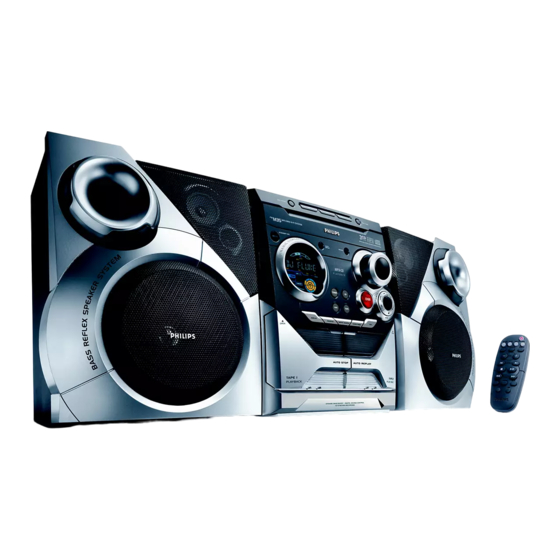
Mini System
Service
Service
Service
Service
Service
Service Manual
©
Copyright 2005 Philips Consumer Electronics B.V. Eindhoven, The Netherlands
All rights reserved. No part of this publication may be reproduced, stored in a retrieval system or
transmitted, in any form or by any means, electronic, mechanical, photocopying, or otherwise
without the prior permission of Philips.
Published by SL0509 Service Audio
Version 1.0
TABLE OF CONTENTS
Location of PC Boards ................................................ 1-2
Versions Variation & Package .................................... 1-2
Specifications .............................................................. 1-3
Measurement Setup ................................................... 1-4
Service Aids ................................................................ 1-5
ESD & Safety Instruction ............................................ 1-6
Service Instruction ...................................................... 1-7
Setting Procedure & Repair Instructions ....................... 2
Disassembly Instructions & Service positions .............. 3
Block & Wiring Diagram ................................................ 4
Front Board .................................................................... 5
Main Board .................................................................... 6
ETF7 Tape Module ........................................................ 7
Power Board .................................................................. 8
3Cdc-Lc-Mp3Cd2002 Module .................................... 9
Mechanical Exploded View & Parts List ...................... 10
Printed in The Netherlands Subject to modification.
FWM35/
Page
CLASS 1
GB
21/21M/22/30
3141 785 30140
Advertisement
Table of Contents


Need help?
Do you have a question about the FWM35/21 and is the answer not in the manual?
Questions and answers